

Page 1

HM6208H Series
65,536-word × 4-bit High Speed CMOS Static RAM
Features
• Single 5 V supply and high density 24-pin package
• High speed: Access time 25/35/45 ns (max)
• Low power
Operation: 300 mW (typ)
Standby: 100 µW (typ)
30 µW (typ) (L-version)
• Completely static memory required
No clock or timing strobe required
• Equal access and cycle time
• Directly TTL compatible: All inputs and outputs
• Battery backup operation capability (L-version)
Ordering Information
Type No. Access Time Package
HM6208HP-25
HM6208HP-35
HM6208HP-45
HM6208HLP-25
HM6208HLP-35
HM6208HLP-45
HM6208HJP-25
HM6208HJP-35
HM6208HJP-45
HM6208HLJP-25
HM6208HLJP-35
HM6208HLJP-45
25 ns
35 ns
45 ns
25 ns
35 ns
45 ns
25 ns
35 ns
45 ns
25 ns
35 ns
45 ns
300-mil, 24-pin plastic DIP (DP-24NC)
300-mil, 24-pin SOJ (CP-24D)
Page 2
HM6208H Series
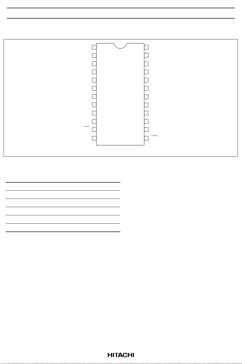
Pin Arrangement
Pin Description
Pin Name Function
A0–A15 Address
I/O1–I/O4 lnput/output
CS Chip select
WE Write enable
V
CC
V
SS
Power supply
Ground
SS
1A0
2A1
3A2
4A3
5A4
6A5
7A6
8A7
9A8
10A9
11CS
12V
(Top view)
24
V
CC
A1523
A1422
A1321
A1220
A1119
A1018
I/O117
I/O216
I/O315
I/O414
WE13
2
Page 3
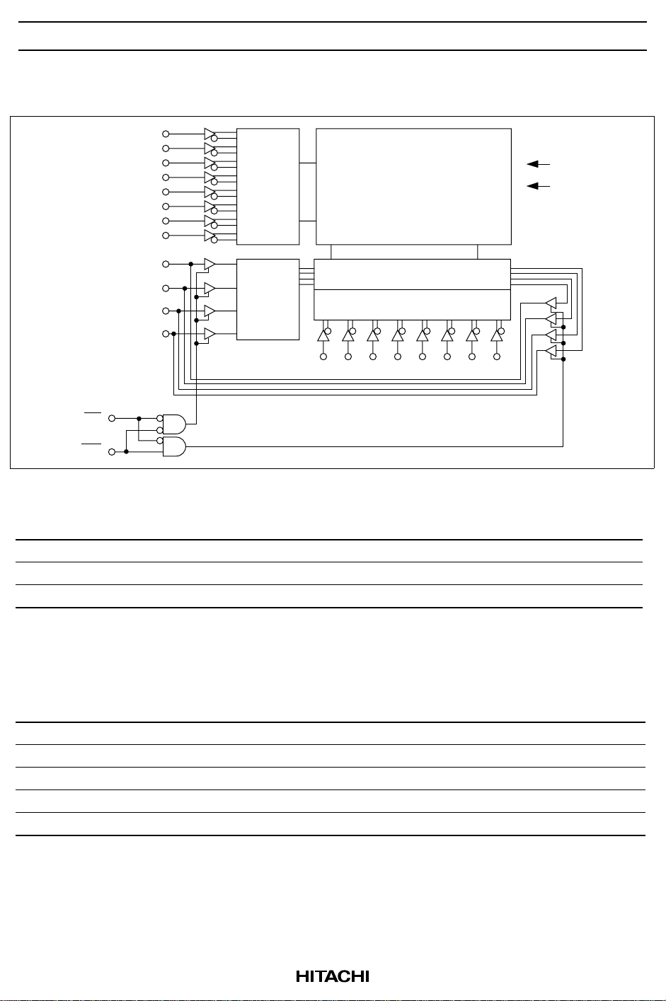
Block Diagram
A14
A15
A0
A1
A2
A3
A4
A5
Row
decoder
Memory array
256 × 1024
HM6208H Series
V
CC
V
SS
I/O1
I/O2
I/O3
Input
data
control
Column I/O
Column decoder
I/O4
A13
A12A11A10 A9 A8 A7 A6
CS
WE
Truth Table
CS WE Mode VCC Current I/O Pin Ref. Cycle
H × Not selected I
L H Read I
L L Write I
Note: ×: Don’t care.
, I
SB
SB1
CC
CC
High-Z —
Dout Read cycle
Din Write cycle
Absolute Maximum Ratings
Parameter Symbol Value Unit
Voltage on any pin relative to V
SS
Power dissipation P
Operating temperature range Topr 0 to +70 °C
Storage temperature range Tstg –55 to +125 °C
Storage temperature range under bias Tbias –10 to +85 °C
Note: 1. Vin min = –2.5 V for pulse widths ≤ 10 ns.
Vin –0.5*1 to +7.0 V
T
1.0 W
3
Page 4
HM6208H Series
Recommended DC Operating Conditions (Ta = 0 to +70°C)
Parameter Symbol Min Typ Max Unit
Supply voltage V
Input high (logic 1) voltage V
Input low (logic 0) voltage V
CC
V
SS
IH
IL
Note: 1. VIL min = –2.0 V for pulse width ≤ 10 ns.
DC Characteristics (Ta = 0 to +70°C, VCC = 5 V ± 10%, VSS = 0 V)
Parameter Symbol Min Typ
Input leakage current I
Output leakage current I
Operating power supply
current
Standby power supply current ISB — 20 40 — 15 30 mA CS = VIH, min cycle
Standby power supply current
(1)
Output low voltage V
Output high voltage V
Notes: 1. L-version
2. Typical values are at V
LI
LO
I
CC
I
CC1
ISB1 — 0.02 2.0 — 0.02 2.0 CS ≥ VCC – 0.2 V,
*1
ISB1
OL
OH
= 5.0 V, Ta = +25°C and not guaranteed.
CC
4.5 5.0 5.5 V
000V
2.2 — 6.0 V
*1 —
–0.5
0.8 V
HM6208H-25 HM6208H-35/45
*2
Max Min Typ*2Max Unit Test Conditions
— — 2.0 — — 2.0 µAVCC = Max
Vin = V
— — 10.0 — — 10.0 µA CS = VIH, V
= VSS to V
— 60 120 — 50 100 mA CS = V
to V
SS
IL, II/O
CC
IO
CC
= 0 mA,
min cycle,
duty = 100%
— 40 80 — 40 80 mA CS = V
IL, II/O
= 0 mA,
t cycle = 50 ns,
duty = 100%
0 V ≤ Vin < 0.2 V, or
— 0.006 0.1*1— 0.006 0.1
Vin ≥ V
*1
– 0.2 V
CC
— — 0.4 — — 0.4 V IOL = 8 mA
2.4 — — 2.4 — — V IOH = –4.0 mA
Capacitance (Ta = 25°C, f = 1 MHz)
*1
Parameter Symbol Min Max Unit Test Conditions
Input capacitance Cin — 6 pF Vin = 0 V
Input/output capacitance C
I/O
—11pFV
I/O
= 0 V
Note: 1. These parameters are sampled and not 100% tested.
4
Page 5

HM6208H Series
AC Characteristics (Ta = 0 to +70°C, VCC = 5 V ± 10%, unless otherwise noted)
Test Conditions
• Input pulse levels: VSS to 3.0 V
• Input rise and fall time: 5 ns
• Input and output timing reference levels: 1.5 V
• Output load: See figure
Output Load
Dout
255 Ω
+ 5 V
480 Ω
30 pF
Dout
*1
255 Ω
+ 5 V
480 Ω
5 pF
*1
Output load (A) Output load (B)
(t
HZ, tLZ, tWZ,
and tOW)
Note: 1. Including scope and jig
Read Cycle
HM6208H-25 HM6208H-35 HM6208H-45
Parameter Symbol Min Max Min Max Min Max Unit
Read cycle time t
Address access time t
Chip select access time t
Output hold from address change t
Chip selection to output in low-Z t
Chip deselection to output in high-Z t
Chip selection to power up time t
Chip deselection to power down time t
RC
AA
ACS
OH
LZ
HZ
PU
PD
*1
Note: 1. Transition is measured ±200 mV from steady state voltage with load (B). These parameters are
sampled and not 100% tested.
25 — 35 — 45 — ns
—25—35—45ns
—25—35—45ns
5—5—5—ns
5—5—5—ns
*1
015020020ns
0—0—0—ns
—15—25—30ns
5
Page 6

HM6208H Series
Read Timing Waveform (1)
Address
t
OH
t
RC
t
AA
t
OH
Dout
Notes: 1.2.WE is high for read cycle.
Device is continuously selected.
Read Timing Waveform (2)
CS
Dout
V
CC
supply
current
Notes: 1.2.WE is high for read cycle.
I
CC
I
SB
Address valid prior to or coincident with the CS transition to low.
t
ACS
t
LZ
High impedance
t
PU
Valid Data
t
RC
t
HZ
Valid Data
High
t
PD
impedance
50%50%
6
Page 7

HM6208H Series
Write Cycle
HM6208H-25 HM6208H-35 HM6208H-45
Parameter Symbol Min Max Min Max Min Max Unit
Write cycle time t
Chip selection to end of write t
Address valid to end of write t
Address setup time t
Write pulse width t
Write recovery time t
Data valid to end of write t
Data hold time t
Write enabled to output in high-Z t
Output active from end of write t
WC
CW
AW
AS
WP
WR
DW
DH
WZ
OW
Note: 1. Transition is measured ±200 mV from high impedance voltage with load (B).
These parameters are sampled and not 100% tested.
25 — 35 — 45 — ns
20 — 30 — 40 — ns
20 — 30 — 40 — ns
0—0—0—ns
20 — 25 — 30 — ns
3—3—3—ns
15 — 20 — 20 — ns
0—0—0—ns
*1
08010015ns
*1
0—0—0—ns
7
Page 8

HM6208H Series
Write Timing Waveform (1) (WE Controlled)
Address
CS
t
AW
t
AS
WE
t
CW
t
WC
t
WP
*2
t
WR
*1
*4
t
t
DW
DH
Din
Dout
Notes: 1.
t
WZ
Valid Data
*3
t
OW
*4
t
OH
*5
High impedance
A write occurs during the overlap of a low CS and a low WE (t
t
2.
is measured from the earlier of CS or WE going high to the end of the write cycle.
WR
3.
During this period, I/O pins are in the output state. The input signals of the opposite
WP
).
phase to the outputs must not be applied.
4.
If CS is low during this period, I/O pins are in the output state. The data input signals of
opposite phase to the outputs must not be applied to them.
5.
Dout is the same phase of write data of this write cycle.
8
Page 9

Write Timing Waveform (2) (CS Controlled)
Address
t
AS
CS
WE
t
AW
t
WC
t
t
WP
CW
HM6208H Series
*2
t
WR
*1
Din
Dout
Notes: 1.
2.
3.
t
DW
t
DH
Valid Data
High impedance
*3
A write occurs during the overlap of a low CS and a low WE (tWP).
t
is measured from the earlier of CS or WE going high to the end of the write cycle.
WR
If the CS low transition occurs simultaneously with the WE low transition or after the WE
transition, the output buffers remain in a high-impedance state.
9
Page 10

HM6208H Series
Low VCC Data Retention Characteristics (Ta = 0 to +70°C)
These characteristics are guaranteed for the L-version only.
Parameter Symbol Min Typ Max Unit Test Conditions
for data retention V
V
CC
Data retention current I
Chip deselect to data retention time t
Operation recovery time t
DR
CCDR
CDR
R
Note: 1. VCC = 3.0 V
Low VCC Data Retention Timing Waveform
2.0 — — V CS ≥ VCC – 0.2 V,
Vin ≥ V
– 0.2 V, or
CC
0 V ≤ Vin < 0.2 V,or
—2 50*1µA
0 ——ns
5 ——ms
V
CC
CS
4.5 V
2.2 V
V
DR
0 V
t
CDR
Data retention mode
CS ≥ VCC – 0.2 V
t
R
10
Page 11

HM6208H Series
Package Dimensions
HM6208HP/HLP Series (DP-24NC) Unit: mm
29.88
1
1.14
1.27 Max
2.54 ± 0.25
30.48 Max
1.30
0.48 ± 0.10
1324
12
7.10
7.40 Max
5.08 Max
2.54 Min
0.51 Min
0.25
0° – 15°
7.62
+ 0.11
– 0.05
HM6208HJP/HLJP Series (CP-24D) Unit: mm
15.63
16.00 Max
1.27
0.10
13
12
8.64 ± 0.13
7.62 ± 0.13
+0.25
3.50 ± 0.26
–0.17
0.80
6.76
+ 0.35
– 0.16
+ 0.21
– 0.24
2.40
24
1
0.43 ± 0.10
0.74
1.30 Max
11
 Loading...