

Page 1

查询HD61830供应商
Description
The HD61830/HD61830B is a dot matrix liquid crystal graphic display controller LSI that stores the
display data sent from an 8-bit microcontroller in the external RAM to generate dot matrix liquid crystal
driving signals.
HD61830/HD61830B
LCDC (LCD Timing Controller)
ADE-207-275(Z)
'99.9
Rev. 0.0
It has a graphic mode in which 1-bit data in the external RAM corresponds to the on/off state of 1 dot on
liquid crystal display and a character mode in which characters are displayed by storing character codes in
the external RAM and developing them into the dot patterns with the internal character generator ROM.
Both modes can be provided for various applications.
The HD61830/HD61830B is produced by the CMOS process. Thus, combined with a CMOS
microcontroller it can complete a liquid crystal display device with lower power dissipation.
Features
• Dot matrix liquid crystal graphic display controller
• Display control capacity
Graphic mode: 512k dots (216 bytes)
Character mode: 4096 characters (212 characters)
• Internal character generator ROM: 7360 bits
160 types of 5 × 7 dot characters
32 types of 5 × 11 dot characters
Total 192 characters
Can be extended to 256 characters (4 kbytes max.) with external ROM
1
Page 2

HD61830/HD61830B
• Interfaces to 8-bit MPU
• Display duty cycle (can be selected by a program)
Static to 1/128 duty cycle
• Various instruction functions
Scroll, cursor on/off/blink, character blink, bit manipulation
• Display method: Selectable A or B types
• Internal oscillator (with external resistor and capacitor) HD61830
• Operating frequency
1.1 MHz HD61830
2.4 MHz HD61830B
• Low power dissipation
• Power supply: Single +5 V ±10%
• CMOS process
2
Page 3
HD61830/HD61830B
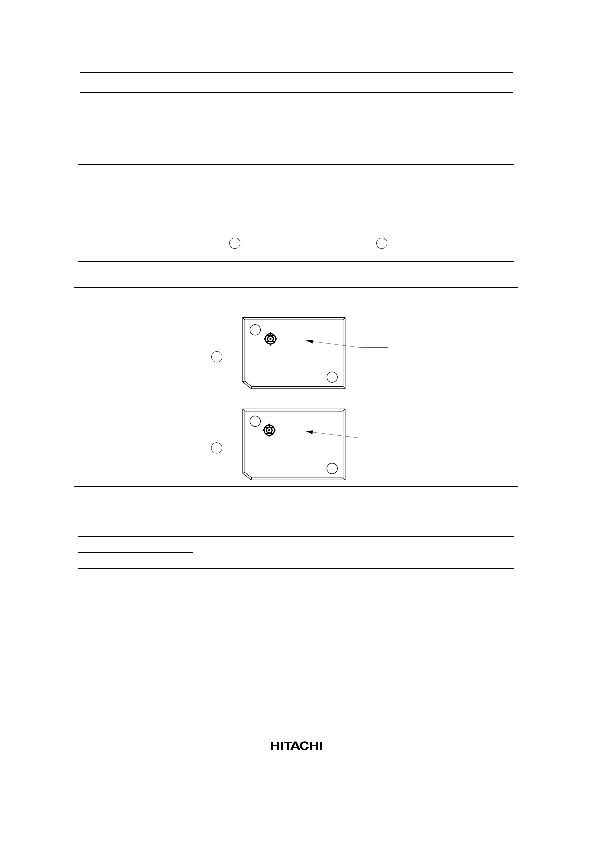
Differences between Products
HD61830 and HD61830B
HD61830 HD61830B
Oscillator Internal or external External only
Operating frequency 1.1 MHz 2.4 MHz
Pin arrangement
and signal name
Package marking
to see figure
Pin 6: C
Pin 7: R
Pin 9: CPO
A
Package Marking
Pin 6: CE
Pin 7: OE
Pin 9: NC
B
3D13
A
B
HD61830A00
3D13
HD61830B00
Ordering Information
Type No. Package
HD61830A00H 60-pin plastic QFP (FP-60)
HD61830B00H
Lot No.
JAPAN
Lot No.
JAPAN
3
Page 4
HD61830/HD61830B
Pin Arrangement
MB
5
MA0
4
MA1
3
MA2
2
MA3
1
MA4
60
MA5
59
MA6
58
MA7
57
MA8
56
MA9
55
54
MA10
(CE) C
(OE) R
CR
(NC) CPO
FLM
CL1
SYNC
WE
RES
CS
R/W
RS
MA
GND
DB7
DB6
6
7
8
9
10
11
12
13
14
15
E
16
17
18
19
20
21
22
FP-60
(Top view)
53
52
51
50
49
48
47
46
45
44
43
42
41
40
39
38
37
MA11
MA12
MA13
MA14
MA15
D2
D1
CL2
RD0
RD1
RD2
RD3
RD4
RD5
RD6
RD7
MD0
( ) is for HD61830B
4
DB5
23
24
DB4
25
DB3
26
DB2
27
DB1
28
DB0
29
V
CC
30
MD7
31
MD6
32
MD5
33
MD4
34
MD3
36
35
MD2
MD1
Page 5

HD61830/HD61830B
Terminal Functions
Symbol Pin Number I/O Function
DB0–DB7 28–21 I/O Data bus: Three-state I/O common terminal
CS 15 I Chip select: Selected state with CS = 0
R/W 17 I Read/Write:R/W = 1: MPU ← HD61830
RS 18 I Register select:RS = 1: Instruction register
E 16 I Enable: Data is written at the fall of E
CR 8 I CR oscillator (HD61830), External clock input (HD61830B)
C 6 — CR oscillator to capacitor (HD61830 only)
R 7 — CR oscillator to resistor (HD61830 only)
CPO 9 O Clock signal for HD61830 in slave mode (HD61830 only)
CE 6 O Chip enable (HD61830B only)
OE 7 O Output enable (HD61830B only)
NC 9 Open Unused terminal. Don’t connect any wires to this terminal
MA0–MA15 4–1, 60–49 O External RAM address output
MD0–MD7 37–30 I/O Display data bus: Three-state I/O common terminal
RD0–RD7 45–38 I ROM data input: Dot data from external character generator is input
WE 13 O Write enable: Write signal for external RAM
CL2 46 O Display data shift clock for LCD drivers
CL1 11 O Display data latch signal for LCD drivers
FLM 10 O Frame signal for display synchronization
MA 19 O Signal for converting liquid crystal driving signal into AC, A type
MB 5 O Signal for converting liquid crystal driving signal into AC, B type
D1 47 O Display data serial output
D2 48
Data is transferred to MPU through DB0 to DB7.
R/W = 0: MPU → HD61830
RS = 0: Data register
Data can be read while E is 1
CE = 0: Chip enables make external RAM in active
OE = 1: Output enable informs external RAM that HD61830B requires
data bus
(HD61830B only)
In character mode, the line code for external CG is output through
MA12 to MA15 (0: Character 1st line, F: Character 16th line)
D1: For upper half of screen
D2: For lower half of screen
SYNC 12 I/O Synchronous signal for parallel operation
Three-state I/O common terminal (with pull-up MOS)
Master: Synchronous signal is output
Slave: Synchronous signal is input
RES 14 I Reset: Reset = 0 results in display off, slave mode and Hp = 6
5
Page 6
HD61830/HD61830B
Block Diagram
(CE)
CL1 MAMB FLM
WE
(OE)
16
16
(RAC1)
counter (1)
Refesh address
Dot counter
RAM
counter (2)
Refesh address
(DC)
MD0–MD7
*
Multiplexer
16
(CAC)
(RAC2)
counter
Cursor address
8
(DR)
Dot registers
ROM
external
Extended
Character
4
counter
Line address
8
6
8
ROM
generator
(CGROM)
Cursor
RD0–RD7
signal
generator
Mode
control
Multiplexer
Control
signal
(MCR)
register
D1
converter
Parallel/serial
D2
Parallel/serial
circuit
Oscillator
converter
are applied to RAM, MA12 –MA15 are applied to
extended external ROM.
* When extended external ROM is used, MA0–MA11
(CR)
(CL2)
( ) is for HD61830B
SYNC
Data
input
8
(DIR)
register
CSERS
DB0–DB7
Data
output
register
I/O interface circuit
R/W
RES
(DOR)
Control
signal
(IR)
register
Instruction
4
Busy
flag
Oscillator
(BF)
circuit
CPOR
f
C
f
CL2
6
Page 7

HD61830/HD61830B
Block Functions
Registers
The HD61830/HD61830B has the five types of registers: instruction register (IR), data input register (DIR),
data output register (DOR), dot registers (DR), and mode control register (MCR).
The IR is a 4-bit register that stores the instruction codes for specifying MCR, DR, a start address register,
a cursor address register, and so on. The lower order 4 bits DB0 to DB3 of data buses are written in it.
The DIR is an 8-bit register used to temporarily store the data written into the external RAM, DR, MCR,
and so on.
The DOR is an 8-bit register used to temporarily store the data read from the external RAM. Cursor address
information is written into the cursor address counter (CAC) through the DIR. When the memory read
instruction is set in the IR (latched at the falling edge of E signal), the data of external RAM is read to DOR
by an internal operation. The data is transferred to the MPU by reading the DOR with the next instruction
(the contents of DOR are output to the data bus when E is at the high level).
The DR are registers used to store dot information such as character pitches and the number of vertical
dots, and so on. The information sent from the MPU is written into the DR via the DIR.
The MCR is a 6-bit register used to store the data which specifies states of display such as display on/off
and cursor on/off/blink. The information sent from the MPU is written in it via the DIR.
Busy Flag (BF)
The busy flag = 1 indicates the HD61830 is performing an internal operation. Instructions cannot be
accepted. As shown in Control Instruction, read busy flag, the busy flag is output on DB7 under the
conditions of RS = 1, R/W = 1, and E = 1. Make sure the busy flag is 0 before writing the next instruction.
Dot Counters (DC)
The dot counters are counters that generate liquid crystal display timing according to the contents of DR.
7
Page 8

HD61830/HD61830B
Refresh Address Counters (RAC1/RAC2)
The refresh address counters, RAC1 and RAC2, control the addresses of external RAM, character generator
ROM (CGROM), and extended external ROM. The RAC1 is used for the upper half of the screen and the
RAC2 for the lower half. In the graphic mode, 16-bit data is output and used as the address signal of
external RAM. In the character mode, the high order 4 bits (MA12–MA15) are ignored. The 4 bits of line
address counter are output instead and used as the address of extended ROM.
Character Generator ROM
The character generator ROM has 7360 bits in total and stores 192 types of character data. A character code
(8 bits) from the external RAM and a line code (4 bits) from the line address counter are applied to its
address signals, and it outputs 5-bit dot data.
The character font is 5 × 7 (160 characters) or 5 × 11 (32 characters). The use of extended ROM allows 8 ×
16 (256 characters max.) to be used.
Cursor Address Counter
The cursor address counter is a 16-bit counter that can be preset by instruction. It holds an address when the
data of external RAM is read or written (when display dot data or a character code is read or written). The
value of the cursor address counter is automatically increased by 1 after the display data is read or written
and after the set/clear bit instruction is executed.
Cursor Signal Generator
The cursor can be displayed by instruction in character mode. The cursor is automatically generated on the
display specified by the cursor address and cursor position.
Parallel/Serial Conversion
The parallel data sent from the external RAM, character generator ROM, or extended ROM is converted
into serial data by two parallel/serial conversion circuits and transferred to the liquid crystal driver circuits
for upper screen and lower screen simultaneously.
8
Page 9
HD61830/HD61830B
y
Display Control Instructions
Display is controlled by writing data into the instruction register and 13 data registers. The RS signal
distinguishes the instruction register from the data registers. 8-bit data is written into the instruction register
with RS = 1, and the data register code is specified. After that, the 8-bit data is written in the data register
and the specified instruction is executed with RS = 0.
During the execution of the instruction, no new instruction can be accepted. Since the busy flag is set
during this, read the busy flag and make sure it is 0 before writing the next instruction.
1. Mode Control: (Execution time: 4 µs) Code H'00 (hexadecimal) written into the instruction register
specifies the mode control register.
Register
Instruction reg.
Mode control reg.
DB5 DB4 DB3 DB2 DB1 DB0 Cursor/blink CG
1/0 1/0 0
0
1
1
0
0
1
1
0
0
1
0
1
0
1
0
1
0
R/W
0
0
RS
DB7
1
0
0
1
0
1
0
DB6
0
0
Cursor off
Cursor on
Cursor off, character blink
Cursor blink
Cursor off
Cursor on
Cursor off, character blink
Cursor blink
DB50DB40DB30DB20DB10DB0
0
0
Mode data
0
Graphic/character
display
Character display
(Character mode)
Internal CGExternal CG
Graphic mode
Display ON/OFF
Master/slave
Blink
Cursor
Graphic/character
mode
1: Master mode
0: Slave mode
1: Display ON
0: Displa
OFF
Ext./Int. CG
9
Page 10
HD61830/HD61830B
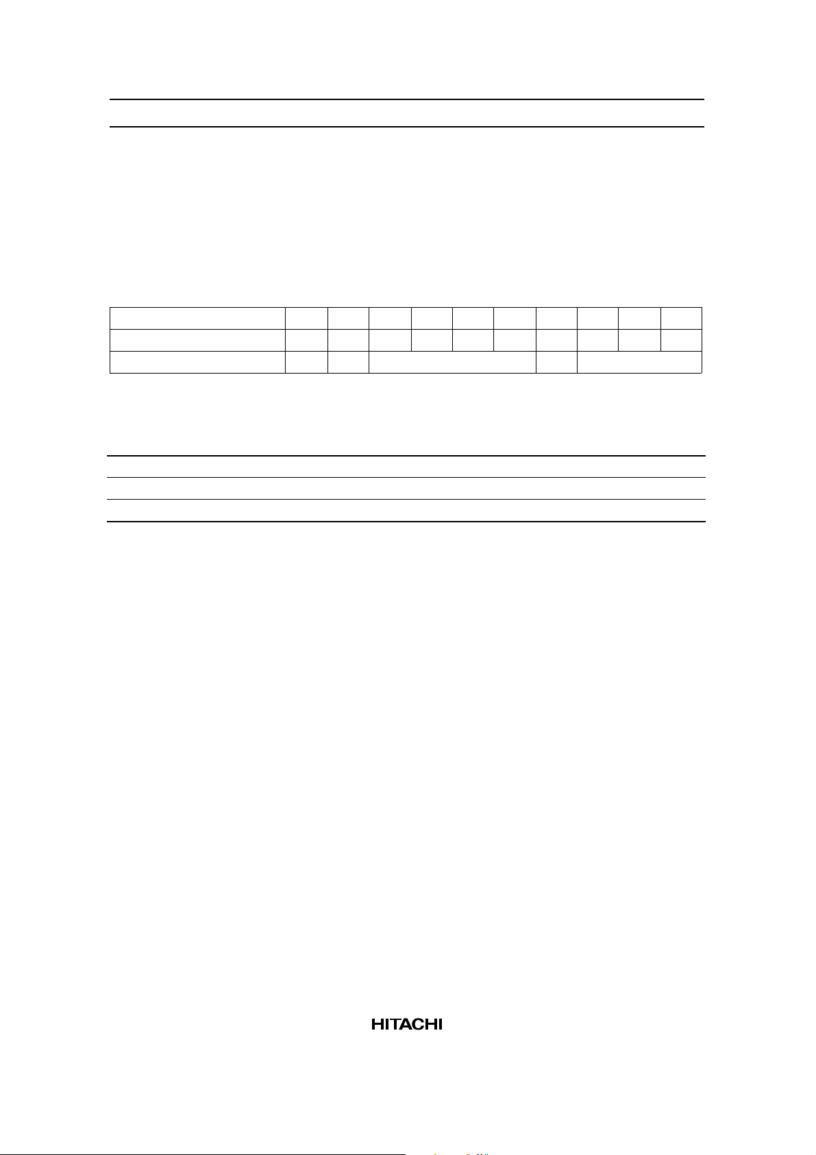
2. Set Character Pitch: (Execution time: 4 µs) Vp indicates the number of vertical dots per character. The
space between the vertically-displayed characters is included in the determination. This value is meaningful
only during character display (in the character mode) and becomes invalid in the graphic mode.
Hp indicates the number of horizontal dots per character in display, including the space between
horizontally-displayed characters. In the graphic mode, the Hp indicates the number of bits of 1-byte display
data to be displayed.
There are three Hp values (Table 1).
Register R/W RS DB7 DB6 DB5 DB4 DB3 DB2 DB1 DB0
Instruction reg. 0 1 0 0 0 0 0 0 0 1
Character pitch reg. 0 0 (Vp – 1) binary 0 (Hp – 1) binary
Table 1 Hp Values
H
p
61016
71107
81118
DB2 DB1 DB0 Horizontal Character Pitch
10
Page 11
HD61830/HD61830B
3. Set Number of Characters: (Execution time: 4 µs) HN indicates the number of horizontal characters in
the character mode or the number of horizontal bytes in the graphic mode. If the total sum of horizontal
dots on the screen is taken as n,
n = Hp × H
N
HN can be set to an even number from 2 to 128 (decimal).
Register R/W RS DB7 DB6 DB5 DB4 DB3 DB2 DB1 DB0
Instruction reg. 0 1 0 0 0 0 0 0 1 0
Number-of-characters reg. 0 0 0 (HN – 1) binary
4. Set Number of Time Divisions (Inverse of Display Duty Ratio): (Execution time: 4 µs) NX indicates
the number of time divisions in multiplex display.
1/NX is the display duty ratio.
A value of 1 to 128 (decimal) can be set to NX.
Register R/W RS DB7 DB6 DB5 DB4 DB3 DB2 DB1 DB0
Instruction reg. 0 1 0 0 0 0 0 0 1 1
Number-of-time-divisions reg. 0 0 0 (NX – 1) binary
5. Set Cursor Position: (Execution time: 4 µs) Cp indicates the position in a character where the cursor is
displayed in the character mode. For example, in 5 × 7 dot font, the cursor is displayed under a character by
specifying Cp = 8 (decimal). The cursor horizontal length is equal to the horizontal character pitch Hp. A
value of 1 to 16 (decimal) can be set to Cp. If a smaller value than the vertical character pitch Vp is set (C
≤ Vp), and a character overlaps with the cursor, the cursor has higher priority of display (at cursor display
on). If Cp is greater than Vp, no cursor is displayed. The cursor horizontal length is equal to Hp.
p
Register R/W RS DB7 DB6 DB5 DB4 DB3 DB2 DB1 DB0
Instruction reg. 0 1 0 0 0 0 0 1 0 0
Cursor position reg. 0 0 0 0 0 0 (Cp – 1) binary
11
Page 12
HD61830/HD61830B
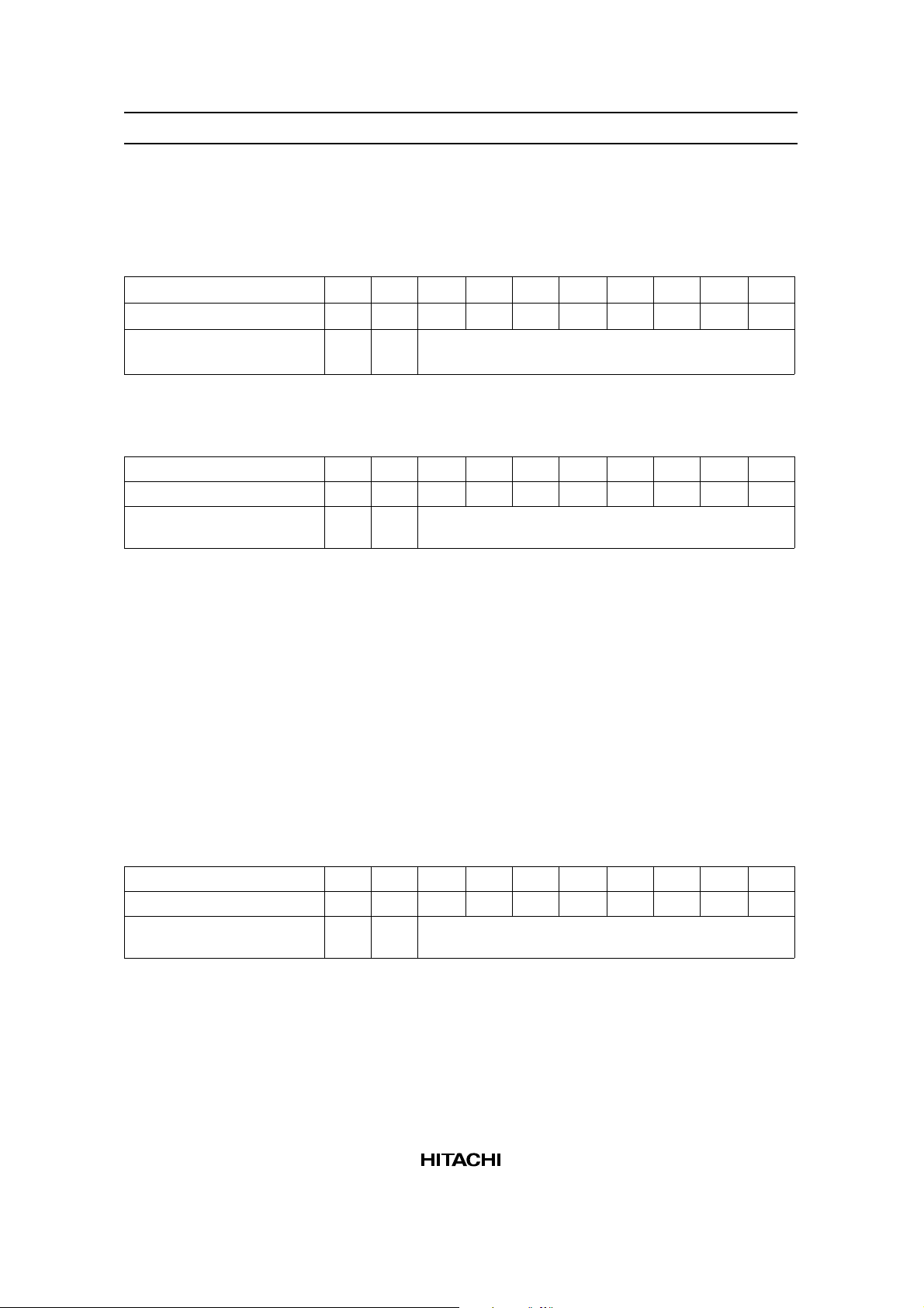
6. Set Display Start Low Order Address: (Execution time: 4 µs) Cause display start addresses to be
written in the display start address registers. The display start address indicates a RAM address at which the
data displayed at the top left end on the screen is stored. In the graphic mode, the start address is composed
of high/low order 16 bits. In the character display, it is composed of the lower 4 bits of high order address
(DB3–DB0) and 8 bits of low order address. The upper 4 bits of high order address are ignored.
Register R/W RS DB7 DB6 DB5 DB4 DB3 DB2 DB1 DB0
Instruction reg. 0 1 0 0 0 0 1 0 0 0
Display start address reg.
(low order byte)
Set Display Start High Order Address
Register R/W RS DB7 DB6 DB5 DB4 DB3 DB2 DB1 DB0
Instruction reg. 0 1 0 0 0 0 1 0 0 1
Display start address reg.
(high order byte)
0 0 (Start low order address) binary
0 0 (Start high order address) binary
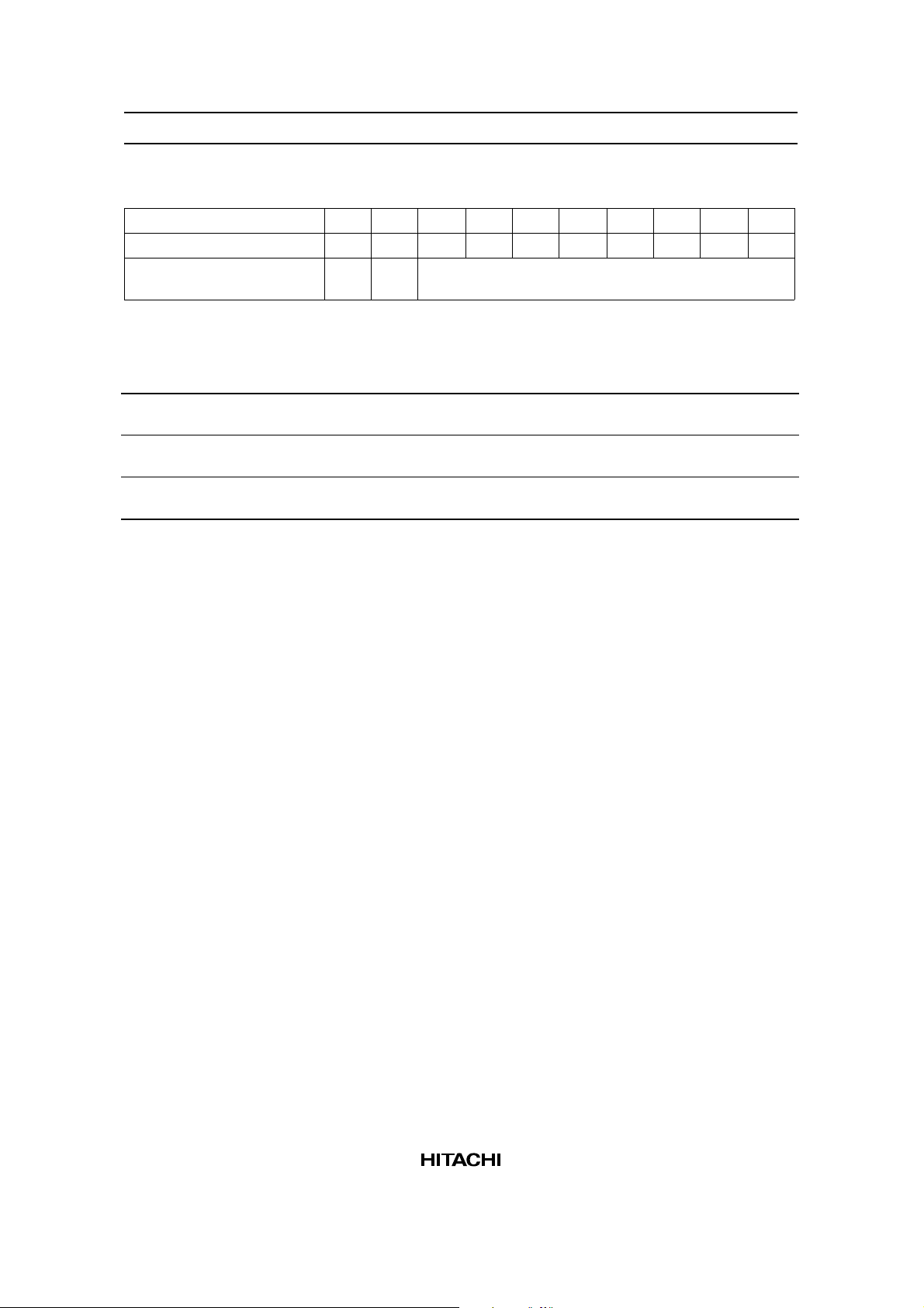
7. Set Cursor Address (Low Order) (RAM Write Low Order Address): (Execution time: 4 µs) Cause
cursor addresses to be written in the cursor address counters. The cursor address indicates an address for
sending or receiving display data and character codes to or from the RAM.
That is, data at the address specified by the cursor address are read/written. In the character mode, the
cursor is displayed at the character specified by the cursor address.
A cursor address consists of the low-order address (8 bits) and the high-order address (8 bits). Satisfy the
following requirements setting the cursor address (Table 2).
The cursor address counter is a 16-bit up-counter with set and reset functions. When bit N changes from 1
to 0, bit N + 1 is incremented by 1. When setting the low order address, the LSB (bit 1) of the high order
address is incremented by 1 if the MSB (bit 8) of the low order address changes from 1 to 0. Therefore, set
both the low order address and the high order address as shown in the Table 2.
Register R/W RS DB7 DB6 DB5 DB4 DB3 DB2 DB1 DB0
Instruction reg. 0 1 0 0 0 0 1 0 1 0
Cursor address counter
(low order byte)
0 0 (Cursor low order address) binary
12
Page 13
HD61830/HD61830B
Set Cursor Address (High Order) (RAM Write High Order Address)
Register R/W RS DB7 DB6 DB5 DB4 DB3 DB2 DB1 DB0
Instruction reg. 0 1 0 0 0 0 1 0 1 1
Cursor address counter
(high order byte)
Table 2 Cursor Address Setting
Condition Requirement
When you want to rewrite (set ) both the low order
address and the high order address.
When you want to rewrite only the low order address. Do not fail to set the high order address again after
When you want to rewrite only the high order address. Set the high order address. You do not have to set
0 0 (Cursor high order address) binary
Set the low order address and then set the high
order address.
setting the low order address.
the low order address again.
13
Page 14

HD61830/HD61830B
8. Write Display Data: (Execution time: 6 µs) After the code $“0C” is written into the instruction register
with RS = 1, 8-bit data with RS = 0 should be written into the data register. This data is transferred to the
RAM specified by the cursor address as display data or character code. The cursor address is increased by 1
after this operation.
Register R/W RS DB7 DB6 DB5 DB4 DB3 DB2 DB1 DB0
Instruction reg. 0 1 0 0 0 0 1 1 0 0
RAM 0 0 MSB (pattern data, character code) LSB
9. Read Display Data: (Execution time: 6 µs) Data can be read from the RAM with RS = 0 after writing
code $“0D” into the instruction register. Figure 1 shows the read procedure.
This instruction outputs the contents of data output register on the data bus (DB0 to DB7) and then
transfers RAM data specified by the cursor address to the data output register, also increasing the cursor
address by 1. After setting the cursor address, correct data is not output at the first read but at the second
one. Thus, make one dummy read when reading data after setting the cursor address.
Register R/W RS DB7 DB6 DB5 DB4 DB3 DB2 DB1 DB0
Instruction reg. 0 1 0 0 0 0 1 1 0 1
RAM 1 0 MSB (pattern data, character code) LSB
CS
E
R/W
RS
DB
Cursor
address
Data output
register
B0AN
Cursor
Busy
check
address
set
mode
Cursor
low
order
address
write
BOBNUB0D
L
Busy
Cursor
Cursor
check
address
set
mode
N
L
high
order
address
write
Busy
check
Figure 1 Read Procedure
Data
read
mode
*
Dummy
read
B (N) B
Busy
checkNaddress
data
read
Busy
check
(N+1)
N + 1
address
data
read
N N + 1 N + 2 N + 3
N address data
N + 1 address data
N + 2
...
14
Page 15

HD61830/HD61830B
10. Clear Bit: (Execution time: 36 µs) The clear/set bit instruction sets 1 bit in a byte of display data RAM
to 0 or 1, respectively. The position of the bit in a byte is specified by NB and RAM address is specified by
cursor address. After the execution of the instruction, the cursor address is automatically increased by 1. N
is a value from 1 to 8. NB = 1 and NB = 8 indicates LSB and MSB, respectively.
Register R/W RS DB7 DB6 DB5 DB4 DB3 DB2 DB1 DB0
Instruction reg. 0 1 0 0 0 0 1 1 1 0
Bit clear reg. 0 0 0 0 0 0 0 (NB – 1) binary
Set Bit
Register R/W RS DB7 DB6 DB5 DB4 DB3 DB2 DB1 DB0
Instruction reg. 0 1 0 0 0 0 1 1 1 1
Bit set reg. 0 0 0 0 0 0 0 (NB – 1) binary
11. Read Busy Flag: (Execution time: 0 µs) When the read mode is set with RS = 1, the busy flag is
output to DB7. The busy flag is set to 1 during the execution of any of the other instructions. After the
execution, it is set to 0. The next instruction can be accepted. No instruction can be accepted when busy
flag = 1. Before executing an instruction or writing data, perform a busy flag check to make sure the busy
flag is 0. When data is written in the register (RS = 1), no busy flag changes. Thus, no busy flag check is
required just after the write operation into the instruction register with RS = 1.
B
The busy flag can be read without specifying any instruction register.
Register R/W RS DB7 DB6 DB5 DB4 DB3 DB2 DB1 DB0
Busy flag 1 1 1/0 *
15
Page 16

HD61830/HD61830B
H
p
RD7RD0
p
V
X
N
STA
CURA
p
C
HN (digit)
16
Symbol
H
p
H
N
Name
Horizontal character pitch
Number of horizontal
characters
Meaning
Horizontal character pitch
Number of horizontal characters per
line (number of digits) in the character
mode or number of bytes per line in
the graphic mode
V
p
C
p
Vertical character pitch Vertical character pitch 1 to 16 dots
Cursor position Line number on which the cursor
can be displayed
N
X
Note:
Number of time divisions Inverse of display duty ratio 1 to 128 lines
If the number of vertical dots on the screen is m, and the number of horizontal dots is n,
1/m = 1/N
n = H
m/V
C
≤ Vp
p
= display duty ratio
X
× HN,
p
= Number of display lines
p
Figure 2 Display Variables
Value
6 to 8 dots
2 to 128 digits
(an even number)
1 to 16 lines
Page 17

Display Mode
HD61830/HD61830B
Display Panel
Liquid Crystal
p
H
RAM
b7 b6 b5 b4 b3 b2 b1 b0
ABC
: 6, 7, or 8 dots
p
H
01000001
01000010
Start
address
p
H
8 dots 8 dots
b0 b7
01010101
b7 b6 b5 b4 b3 b2 b1 b0
11111111
Start
address
: 8 dots
p
H
from MPU
Display Data
Character code
(8 bits)
Display Mode
Character
display
(8 bits)
Graphic Display pattern
17
Page 18

HD61830/HD61830B
Internal Character Generator Patterns and Character Codes
Higher
Lower
4 bits
4 bits
xxxx0000
xxxx0001
xxxx0010
xxxx0011
xxxx0100
xxxx0101
xxxx0110
0010 0011 0100 0101 0110 0111 1010 1011 1100 1101 1110 1111
xxxx0111
xxxx1000
xxxx1001
xxxx1010
xxxx1011
xxxx1100
xxxx1101
xxxx1110
xxxx1111
18
Page 19

HD61830/HD61830B
Example of Correspondence between External CGROM Address Data and
Character Pattern
8 × 8 Dot Font
A6 A5 A4 A3
0000
0001
0010
8 × 16 Dot Font
A10
A 9
A 8
A 7
A2 A1 A0 00 01 02 03 04 05 06 07 00 01 02 03 04 05 06 07
0001111000001110000
0011000100010001000
0101000100010001000
0111111000010001000
1001010000010101000
1011001000010010000
1101000100001101000
1110000000000000000
0001110000100000000
0011010001000000000
0101110010001000001
0110000100000100010
1000001000000010100
1010010011100001000
1100100010100010000
1111000011111110000
000
0
0
0
0
0
0
0
1
0
0
1
0
1
1
1
1
A11
A10
A 9
A7 00 01 02 03 04 05 06 07 00 01 02 03 04 05 06 07
A6 A5 A4 A3 A2 A1 A0
0000
0
000
A 8
0000000000 000000111
000000000 0000001000
00000000 00000001001
00000000000000001010
00000000000000001011
00000000000000001100
00000000000000001101
00000000000000001110
00000000000000001111
00000000000000000000
0
0
0
0
000000000000
000 000000000000001
000 000000000000010
0000 00000 00011
0 000000 000 000100
00 000000 0 0000101
000 000000 00000110
0
0
0
1
0
0
1
0
19
Page 20

HD61830/HD61830B
Example of Configuration
Graphic Mode or Character Mode (1) (Internal Character Generator)
MPU
MD0–MD7
HD61830
HD61830B
MA0–MA15 at graphic mode,
MA0–MA11 at character mode
RAM
Character Mode (2) (External Character Generator)
HD61830
ROM
HD61830B
MA12–
MA15
–
MD0
MD7
MA0–MA11
RAM
MPU
RD0–RD7
Liquid crystal
display module
Liquid crystal
display module
20
Page 21

Parallel Operation (HD61830)
(Master)
MPU
CS
CR
CS
Parallel Operation (HD61830B)
(Master)
MPU
HD61830B (1)
CS
HD61830 (1)
CPO
SYNC
SYNC
HD61830 (2)
(Slave)
SYNC
RAM
RAM
RAM
Liquid crystal
display module (1)
Driving both of two
module by same
common signal
Liquid crystal
display module (1)
Driving both of two
module by same
common signal
HD61830/HD61830B
Liquid crystal
display module (2)
Liquid crystal
display module (2)
SYNC
HD61830B (2)
CS
(Slave)
RAM
21
Page 22

HD61830/HD61830B
HD61830 Application (Character Mode, External CG, Character Font 8 × 8)
HD6800
VMA
R/W
+5 V
GND
–5 V
A12
A13
A14
A15
A0
D0
to
D7
ø2
Open
V
CC
HD61830
RS
CS
DB0
to
DB7
E
R/W
SYNC
CPO
RES
RC CR
C
R
WE
MA0
to
MA10
MA11
MA12
to
MA14
MA15
MD0
to
MD7
RD0
to
RD7
FLM
MB
CL1
CL2
D2
MA
D1
HD61830 Application (Graphic Mode)
Open
D0
to
D7
WE
A0
to
A10
RAM (1)
HM6116
A0–A2
CS
ROM
HN462716
OE
A3–A10
OE
CE
WE
A0
to
A10
D1
FLM
M
CL1
CL2
D2
+5 V
GND
–5 V
V0
RAM (2)
HM6116
CS
LCD module
OE
HD6800
MPU
DB0–DB7
CS E
RS R/W
RES
HD61830
controller
MA0–
MA15
MD0–MD7
RAM
16 kbits
CMOS
D1
D2
CL1, CL2
MB, FLM
WE
GND
VDD (5 V)
(–5 V)
V
EE
Segment
driver
Common
Segment
V1 – V6
Power supply for
liquid crystal
display drive
driver
driver
LCD
Segment
driver
Segment
driver
22
Page 23

HD61830/HD61830B
HD61830B Application (Character Mode, External CG, Character Font 8 × 8)
HD6303 HD61830B
+5 V
GND
–5 V
A1
A15
R/W
A0
to
Decoder
D0
to
D7
E
External
clock
Open
RS
CS
DB0
to
DB7
E
R/W
SYNC
V
RES
CC
CR
WE
MA0
to
MA10
OE
CE
MA11
MA12
to
MA15
MD0
to
MD7
RD0
to
RD7
FLM
MB
CL1
CL2
MA
WE
A0
to
A10
A0–A3
D0
to
D7
D1
D2
Open
RAM (1)
HM6116
HN482732A
CS
ROM
OE
D0
to
D7
A4–A11
OE
CE
WE
A0
to
A10
D1
FLM
M
CL1
CL2
D2
+5 V
GND
–5 V
V0
RAM (2)
HM6116
LCD module
CS
OE
D0
to
D7
HD61830B Application (Graphic Mode)
D1
D2
CL1, CL2
MB, FLM
WE
GND
VDD (5 V)
(–5 V)
V
EE
HD6303
MPU
DB0–DB7
CS E
RS R/W
RES
CE
OE
HD61830B
controller
MA0–
MA15
MD0–MD7
RAM
16 kbits
CMOS
Segment
driver
Common
Segment
V1 – V6
Power supply for
liquid crystal
display drive
driver
driver
LCD
Segment
driver
Segment
driver
23
Page 24

HD61830/HD61830B
HD61830 Absolute Maximum Ratings
Item Symbol Value Unit Notes
Supply voltage V
CC
Terminal voltage VT –0.3 to VCC +0.3 V 1, 2
Operating temperature T
Storage temperature T
opr
stg
Notes: 1. All voltages are referenced to GND = 0 V.
2. If LSIs are used beyond absolute maximum ratings, they may be permanently destroyed.
We strongly recommend that you use the LSIs within electrical characteristic limits for normal
operation, because use beyond these conditions will cause malfunction and poor reliability.
–0.3 to +0.7 V 1, 2
–20 to +75 °C
–55 to +125 °C
24
Page 25

HD61830/HD61830B
HD61830 Electrical Characteristics (VCC = 5 V ±10%, GND = 0 V, Ta = –20 to
+75°C)
Item Symbol Min Typ Max Unit Test Condition Notes
Input high voltage (TTL) VIH 2.2 — V
CC
Input low voltage (TTL) VIL 0 — 0.8 V 2
Input high voltage VIHR 3.0 — V
CC
Input high voltage (CMOS) VIHC 0.7 VCC—VCCV4
Input low voltage (CMOS) VILC 0 — 0.3 VCCV4
Output high voltage (TTL) VOH 2.4 — V
CC
Output low voltage (TTL) VOL 0 — 0.4 V IOL = 1.6 mA 5
Output high voltage (CMOS) VOHC VCC – 0.4 — V
CC
Output low voltage (CMOS) VOLC 0 — 0.4 V IOL = 0.6 mA 6
Input leakage current I
Three-state leakage current I
IN
TSL
–5 — 5 µA VIN = 0 – V
–10 — 10 µA VOUT = 0 – VCC8
Power dissipation (1) PW1 — 10 15 mW CR oscillation
Power dissipation (2) PW2 — 20 30 mW External clock
Internal clock operation
f
osc
400 500 600 kHz Cf = 15 pF ±5%
(Clock oscillation frequency)
External clock operation
f
cp
100 500 1100 kHz 11
(External clock operating frequency)
External clock duty Duty 47.5 50 52.5 % 11
External clock rise time t
External clock fall time t
Pull-up current I
rcp
fcp
PL
— — 0.05 µs11
— — 0.05 µs11
21020µA VIN = GND 12
Notes: The I/O terminals have the following configuration:
1. Applied to input terminals and I/O common terminals, except terminals SYNC, CR, and RES.
2. Applied to input terminals and I/O common terminals, except terminals SYNC and CR.
3. Applied to terminal RES.
4. Applied to terminals SYNC and CR.
5. Applied to terminals DB0–DB7, WE, MA0–MA15, and MD0–MD7.
6. Applied to terminals SYNC, CP0, FLM, CL1, CL2, D1, D2, MA, and MB.
7. Applied to input terminals.
8. Applied to I/O common terminals. However, the current which flows into the output drive MOS is
excluded.
V1
V3
V–IOH = 0.6 mA 5
V–IOH = 0.6 mA 6
7
CC
9
f
= 500 kHz
osc
9
f
= 1 MHz
cp
10
R
= 39 kΩ ±2%
f
25
Page 26

HD61830/HD61830B
9. The current which flows into the input and output circuits is excluded. When the input of CMOS is
in the intermediate level, current flows through the input circuit, resulting in the increase of power
supply current. To avoid this, input must be fixed at high or low.
The relationship between the operating frequency and the power dissipation is given below.
50
(mW)
W
P
40
Max
30
Typ
20
10
0
250 500 750 1000 1250 1500
(kHz)
f
OSC
10.Applied to the operation of the internal oscillator when oscillation resistor Rf and oscillation
capacity C
R
f
are used.
f
C
f
R
C
Cf = 15 pF ±5%
R
= 39 kΩ±2%
f
(when f
OSC
=
500 kHz typ)
CR
The relationship among oscillation frequency, R
T
= 25°C, VCC = 5 V
f
OSC
(kHz)
a
and Cf is given below.
f
800
26
600
400
200
= 10 pF
C
f
C
= 15 pF
f
0
40 60 80 100 120 140 160 180
R
(kΩ)
f
Page 27

11.Applied to external clock operation.
HD61830/HD61830B
Open
Open
Oscillator
R
C
CR
0.7 V
0.5 V
0.3 V
CC
CC
CC
12.Applied to SYNC, DB0–DB7, and RD0–RD7.
fcp
T
I
T
Duty cycle = × 100%
h
Th + T
I
T
h
t
rcp
t
27
Page 28

HD61830/HD61830B
Input Terminal
Applicable terminal: CS, E, RS, R/W, RES, CR (without pull-up MOS)
V
CC
PMOS
NMOS
Applicable terminal: RD0–RD7 (with pull-up MOS)
V
CC
PMOS PMOS
(Pull-up MOS)
V
CC
NMOS
28
Page 29

HD61830/HD61830B
Output Terminal
Applicable terminal: CL1, CL2, MA, MB, FLM, D1, D2, WE, CPO, MA0–MA15
V
CC
PMOS
NMOS
I/O Common Terminal
Applicable terminal: DB0–DB7, SYNC, MD0–MD7 (MD0–MD7 have no pull-up MOS)
(Pull-up MOS)
V
CC
PMOS PMOS
V
Input circuit
CC
NMOS
V
CC
PMOS
NMOS
Output circuit
(Three state)
Enable
Data
29
Page 30

HD61830/HD61830B
Timing Characteristics
HD61830 MPU Interface (VCC = 5 V ±10%, GND = 0 V, Ta = –20 to +75°C)
Item Symbol Min Typ Max Unit
Enable cycle time t
Enable pulse width High level t
Low level t
Enable rise time t
Enable fall time t
Setup time t
Data setup time t
Data delay time t
Data hold time t
Address hold time t
Output data hold time t
CYC
WEH
WEL
Er
Ef
AS
DSW
DDR
DHW
AH
DH
Note: * The following load circuit is connected for specification:
E
CS, R/W, RS
2.2 V
0.8 V
t
AS
2.2 V
0.8 V
1.0 — — µs
0.45 — — µs
0.45 — — µs
——25ns
——25ns
140 — — ns
225 — — ns
— — 225 ns *
10 — — ns
10 — — ns
20 — — ns
t
CYC
t
WEH
t
Er
t
DSW
t
Ef
t
DHW
t
WEL
t
AH
30
DB0–DB7
(MPU→HD61830)
DB0–DB7
(MPU←HD61830)
Test point
D1
CR
2.2 V
0.8 V
t
DDR
t
DH
2.4 V
0.4 V
V
CC
R
L
D2
R
= 2.4 kΩ
L
R = 11 kΩ
D3
C = 130 pF (C includes jig capacitance)
D4
Diodes D1 to D4 : 1S2074
H
Page 31

HD61830/HD61830B
y
HD61830 External RAM and ROM Interface (VCC = 5 V ±10%, GND = 0 V, Ta = –20 to +75°C)
Item Symbol Min Typ Max Unit
SYNC delay time t
SYNC pulse width Low level t
CPO cycle time t
CPO pulse width High level t
Low level t
MA0 to MA15 refresh delay time t
MA0 to MA15 write address delay time t
MD0 to MD7 write data delay time t
MD0 to MD7, RD0 to RD7 setup time t
Memory address setup time t
Memory data setup time t
WE delay time t
WE pulse width (low level) t
DSY
WSY
CCPO
WCPOH
WCPOL
DMAR
DMAW
DMDW
SMD
SMAW
SMDW
DWE
WWE
— — 200 ns
900 — — ns
900 — — ns
450 — — ns
450 — — ns
— — 200 ns
— — 200 ns
— — 200 ns
900 — — ns
250 — — ns
250 — — ns
— — 200 ns
450 — — ns
1
V
SYNC
t
DSY
CPO
MA0–MA15
MD0–MD7
RD0–RD7
2
t
WSY
CC
t
t
DMAR
WCPOL
t
1
2
2.4 V
0.4 V
CCPO
V
CC
*
2.2 V
0.8 V
*
2.2 V
0.8 V
t
WCPOH
t
SMD
t
SMD
t
DMAR
2.2 V
0.8 V
WE
Notes: 1.2.No load is applied to all the output terminals.
“*” indicates the dela
time of RAM and ROM.
t
DMAW
*
t
SMAW
2.4 V
0.4 V
t
DMDW
*
t
SMDW
2.4 V
0.4 V
t
DWE
t
WWE
31
Page 32

HD61830/HD61830B
HD61830 LCD Driver Interface (V
= 5 V ±10%, GND = 0 V, Ta = –20 to +75°C)
CC
Item Symbol Min Typ Max Unit
Clock pulse width (high level) t
Clock delay time t
Clock cycle time t
Clock pulse width High level t
Low level t
MA, MB delay time t
FLM delay time t
Data delay time t
Data setup time t
WCL1
DCL2
WCL2
WCH
WCL
DM
DF
DD
SD
450 — — ns
— — 200 ns
900 — — ns
450 — — ns
450 — — ns
— — 300 ns
— — 300 ns
— — 200 ns
250 — — ns
Note: No load is applied to all the output terminals (MA, MB, FLM, D1, and D2).
t
WCL1
1
CL1
2
t
DCL2
V
CC
t
WCL2
CL2
MA, MB
FLM
D1
D2
1
V
CC
2
t
WCH
1
2
t
DM
1
V
CC
2
t
t
DD
SD
1
V
CC
2
t
WCL
V
CC
t
DF
32
Page 33

HD61830/HD61830B
HD61830B Absolute Maximum Ratings
Item Symbol Value Unit Notes
Supply voltage V
CC
Terminal voltage VT –0.3 to V
Operating temperature T
Storage temperature T
opr
stg
Notes: 1. All voltage is referred to GND = 0 V.
2. If LSIs are used beyond absolute maximum ratings, they may be permanently destroyed.
We strongly recommend that you use the LSIs within electrical characteristic limits for normal
operation, because use beyond these conditions will cause malfunction and poor reliability.
–0.3 to +0.7 V 1, 2
+0.3 V 1, 2
CC
–20 to +75 °C
–55 to +125 °C
33
Page 34

HD61830/HD61830B
HD61830B Electrical Characteristics (VCC = 5V ±10%, GND = 0V, Ta = –20 to
+75°C)
Item Symbol Min Typ Max Unit Test Condition Notes
Input high voltage (TTL) VIH 2.2 — V
CC
Input low voltage (TTL) VIL 0 — 0.8 V 2
Input high voltage VIHR 3.0 — V
Input high voltage (CMOS) VIHC 0.7 V
—VCCV4
CC
CC
Input low voltage (CMOS) VILC 0 — 0.3 V
Output high voltage (TTL) VOH 2.4 — V
CC
Output low voltage (TTL) VOL 0 — 0.4 V I
Output high voltage (CMOS) VOHC V
– 0.4 — V
CC
CC
Output low voltage (CMOS) VOLC 0 — 0.4 V IOI = 0.6 mA 6
Input leakage current I
Three-state leakage current I
Pull-up current I
Power dissipation P
IN
TSL
PL
W
–5 — 5 µA VIN = 0 – V
–10 — 10 µA VOUT = 0 – VCC8
21020µA Vin = GND 9
— — 50 mW External clock
Notes: 1. Applied to input terminals and I/O common terminals, except terminals SYNC, CR, and RES.
2. Applied to input terminals and I/O common terminals, except terminals SYNC and CR.
3. Applied to terminal RES.
4. Applied to terminals SYNC and CR.
5. Applied to terminals DB0–DB7, WE, MA0–MA15, OE, CE, and MD0–MD7.
6. Applied to terminals SYNC, FLM, CL1, CL2, D1, D2, MA, and MB.
7. Applied to input terminals.
8. Applied to I/O common terminals. However, the current which flows into the output drive MOS is
excluded.
9. Applied to SYNC, DB0–DB7, and RD0–RD7.
10.The current which flows into the input and output circuits is excluded. When the input of CMOS is
in the intermediate level, current flows through the input circuit, resulting in the increase of power
supply current. To avoid this, input must be fixed at high or low.
V1
V3
V4
CC
V–IOH = 0.6 mA 5
= 1.6 mA 5
OL
V–IOH = 0.6 mA 6
7
CC
10
f
= 2.4 MHz
cp
34
Page 35

Input Terminal
Applicable terminal: CS, E, RS, R/W, RES, CR (without pull-up MOS)
V
CC
PMOS
NMOS
Applicable terminal: RD0–RD7 (with pull-up MOS)
HD61830/HD61830B
V
CC
PMOS
(Pull-up MOS)
V
CC
PMOS
NMOS
35
Page 36

HD61830/HD61830B
Output Terminal
Applicable terminal: CL1, CL2, MA, MB, FLM, D1, D2, WE, OE, CE, MA0–MA15
V
CC
PMOS
NMOS
I/O Common Terminal
Applicable terminal: DB0–DB7, SYNC, MD0–MD7 (MD0–MD7 have no pull-up MOS)
(Pull-up MOS)
V
CC
PMOS PMOS
V
Input circuit
CC
NMOS
V
CC
PMOS
NMOS
Output circuit
(Three state)
Enable
Data
36
Page 37

HD61830/HD61830B
Timing Characteristics
HD61830B Clock Operation (VCC = 5 V ±10%, GND = 0V, Ta = –20 to +75°C)
Item Symbol Min Typ Max Unit Notes
External clock operating frequency f
cp
External clock duty Duty 47.5 50 52.5 % 1
External clock rise time t
External clock fall time t
SYNC output hold time t
SYNC output delay time t
SYNC input hold time t
SYNC input set-up time t
rcp
fcp
HSYO
DSY
HSYI
SSY
Notes: 1. Applied to external clock input terminal.
CROscillator
2. Applied to SYNC terminal.
100 — 2400 kHz 1
— — 25.0 ns 1
— — 25.0 ns 1
30 — — ns 2, 3
— — 210 ns 2, 3
10 — — ns 2
— — 180 ns 2
0.7 V
0.5 V
0.3 V
CC
CC
CC
T
h
t
rcp
T
l
t
fcp
Duty cycle =
T
h
Th + T
× 100%
l
CR
SYNC
(Output:
at master
mode)
SYNC
(Input:
at slave
mode)
3. Testing load circuit.
Test point
0.7 V
t
HSYI
0.3 V
t
CC
CC
t
DSY
HSYO
0.7 V
0.3 V
0.7 V
0.3 V
t
t
HSYO
CC
CC
t
SSY
CC
C
L
t
HSYI
CC
= 30 pF
C
L
(CL includes jig capacitance)
DSY
t
SSY
37
Page 38

HD61830/HD61830B
HD61830B MPU Interface (VCC = 5V ±10%, GND = 0V, Ta = –20 to +75°C)
Item Symbol Min Typ Max Unit
Enable cycle time t
Enable pulse width High level t
Low level t
Enable rise time t
Enable fall time t
Setup time t
Data setup time t
Data delay time t
Data hold time t
Address hold time t
Output data hold time t
CYC
WEH
WEL
Er
Ef
AS
DSW
DDR
DHW
AH
DH
Note: * The following load circuit is connected for specification:
E
2.2V
0.8V
t
AS
CS, R/W, RS
2.2V
0.8V
1.0 — — µs
0.45 — — µs
0.45 — — µs
— — 25 ns
— — 25 ns
140 — — ns
225 — — ns
— — 225 ns *
10 — — ns
10 — — ns
20 — — ns
t
CYC
t
WEH
t
Er
t
DSW
t
Ef
t
DHW
t
WEL
t
AH
38
DB0–DB7
(MPU→HD61830B)
DB0–DB7
(MPU←HD61830B)
Test point
D1
CR
2.2V
0.8V
t
DDR
t
DH
2.4V
0.4V
V
CC
R
L
D2
D3
D4
= 2.4 kΩ
R
L
R = 11 kΩ
C = 130 pF (C includes jig capacitance)
Diodes D1 to D4 : 1S2074
H
Page 39

HD61830/HD61830B
HD61830B External RAM and ROM Interface (VCC = 5V ±10%, GND = 0V, Ta = –20 to +75°C)
Item Symbol Min Typ Max Unit Notes
MA0–MA15 delay time t
MA0–MA15 hold time t
CE delay time t
CE hold time t
OE delay time t
OE hold time t
MD output delay time t
MD output hold time t
WE delay time t
WE clock pulse width t
MD output high impedance time (1) t
MD output high impedance time (2) t
RD data set-up time t
RD data hold time t
MD data set-up time t
MD data hold time t
Notes: 1. RAM write timing
T
DMA
HMA
DCE
HCE
DOE
HOE
DMD
HMDW
DWE
WWE
ZMDF
ZMDR
SRD
HRD
SMD
HMD
1
— — 300 ns 1, 2, 3
40 — — ns 1, 2, 3
— — 300 ns 1, 2, 3
40 — — ns 1, 2, 3
— — 300 ns 1, 3
40 — — ns 1, 3
— — 150 ns 1, 3
10 — — ns 1, 3
— — 150 ns 1, 3
150 — — ns 1, 3
10 — — ns 1, 3
50 — — ns 1, 3
50——ns2
40——ns2
50——ns2
40——ns2
T
2
T
3
T
1
CR
CE
0–MA15
MA
OE
WE
MD0–MD7
(High impedance)
(output)
T1: Memory data refresh timing for upper screen
T2: Memory data refresh timing for lower screen
T3: Memory read/write timing
0.3 V
t
DMA
t
HMA
t
DOE
t
HOE
CC
t
ZMDR
t
0.7 V
DMD
2.4V
0.6V
CC
t
HCE
0.6V
t
DMA
t
HMA
2.4V
0.6V
t
DOE
t
HOE
2.4V
0.6V
t
t
DWE
DWE
2.4V
0.6V
t
t
HMDW
ZMDF
2.4V
0.6V
t
WWE
Valid
data
39
Page 40

HD61830/HD61830B
2. ROM/RAM read timing
T
1
T
2
T
3
T
1
CR
t
HMD
t
t
t
HCE
HRD
DCE
t
DMA
t
HMA
(*2)
(*3)
t
SMD
t
HMD
(*4)
Invalid data
t
t
HCE
CE
OE
MA0–MA15
MD0–MD7
(input)
RD0–RD7
0.6V
(*2)
2.4V
0.6V
2.2V
0.8V
ba
(*1)
t
DMA
t
HMA
Address for upper screen
Data for the upper screen
2.2V
0.8V
Data for the upper screen
2.4V
0.6V
t
SMD
t
t
HCE
SRD
t
DCE
t
DMA
t
HMA
Address for
the lower screen
t
HMD
the lower screen
t
HRD
t
SMD
Data for
t
SRD
Data for the
lower screen
*1 This figures shows the timing for Hp = 8.
For H
= 7, time shown by “b” becomes zero. For Hp = 6, time shown by “a” and “b”
p
become zero.
Therefore, the number of clock pulses during T1 become 4, 3, or 2 in the case of H
H
= 7, or Hp = 6 respectively.
p
*2 The waveform for instructions with memory read is shown with a dash line. In other cases,
the waveform shown with a solid line is generated.
*3 When an instruction with RAM read/write is executed, the value of cursor address is
output. In other cases, invalid data is output.
*4 When an instruction with RAM read is executed, HD61830B latches the data at this timing.
In other cases, this data is invalid.
3. Test load circuit
t
(*1)
a
DCE
HMA
= 8,
p
40
Test point
D1
CR
V
CC
R
L
D2
D3
D4
= 2.4 kΩ
R
L
R = 11 kΩ
C = 50 pF (C includes jig capacitance)
Diodes D1 to D4 : 1S2074
H
Page 41

HD61830/HD61830B
HD61830B LCD Driver Interface (VCC = 5V ±10%, GND = 0V, Ta = –20 to +75°C)
Item Symbol Min Typ Max Unit Notes
Clock cycle time t
Clock pulse width(high level) t
Clock pulse width(low level) t
Data delay time t
Data hold time t
Clock phase difference (1) t
Clock phase difference (2) t
Clock phase difference (3) t
MA, MB delay time t
FLM set-up time t
FLM hold time t
MA set-up time t
MA hold time t
WCL2
WCH
WCL
DD
DH
CL1
CL2
CL3
DM
SF
HF
SMA
HMA
416 — — ns 1, 3
150 — — ns 1, 3
150 — — ns 1, 3
— — 50 ns 1, 3
100 — — ns 1, 3
100 — — ns 1, 3
100 — — ns 1, 3
100 — — ns 1, 3
–200 — 200 ns 1, 3
400 — — ns 2, 3
1000 — — ns 2, 3
400 — — ns 2, 3
1000 — — ns 2, 3
41
Page 42

HD61830/HD61830B
Notes: 1.
t
WCH
0.7 V
CL2
CL1
D1, D2
MA, MB
2.
CL1
0.3 V
CC
CC
t
CL1
t
DD
0.7 V
0.3 V
CC
CC
t
WCL2
t
SF
0.7 V
0.3 V
t
t
WCL
CL2
CC
CC
t
CL3
t
WCH
t
DH
t
DM
0.7 V
CC
0.3 V
CC
0.7 V
CC
0.3 V
CC
t
HF
FLM
MA
3. Test load circuit
0.7 V
0.3 V
Test point
CC
CC
t
SMA
t
HMA
0.7 V
CC
0.3 V
CC
C
C
L
= 100 pF
L
(C
includes jig capacitance)
L
42
Page 43

HD61830/HD61830B
Cautions
1. Hitachi neither warrants nor grants licenses of any rights of Hitachi’s or any third party’s patent,
copyright, trademark, or other intellectual property rights for information contained in this document.
Hitachi bears no responsibility for problems that may arise with third party’s rights, including
intellectual property rights, in connection with use of the information contained in this document.
2. Products and product specifications may be subject to change without notice. Confirm that you have
received the latest product standards or specifications before final design, purchase or use.
3. Hitachi makes every attempt to ensure that its products are of high quality and reliability. However,
contact Hitachi’s sales office before using the product in an application that demands especially high
quality and reliability or where its failure or malfunction may directly threaten human life or cause risk
of bodily injury, such as aerospace, aeronautics, nuclear power, combustion control, transportation,
traffic, safety equipment or medical equipment for life support.
4. Design your application so that the product is used within the ranges guaranteed by Hitachi particularly
for maximum rating, operating supply voltage range, heat radiation characteristics, installation
conditions and other characteristics. Hitachi bears no responsibility for failure or damage when used
beyond the guaranteed ranges. Even within the guaranteed ranges, consider normally foreseeable
failure rates or failure modes in semiconductor devices and employ systemic measures such as failsafes, so that the equipment incorporating Hitachi product does not cause bodily injury, fire or other
consequential damage due to operation of the Hitachi product.
5. This product is not designed to be radiation resistant.
6. No one is permitted to reproduce or duplicate, in any form, the whole or part of this document without
written approval from Hitachi.
7. Contact Hitachi’s sales office for any questions regarding this document or Hitachi semiconductor
products.
Hitachi, Ltd.
Semiconductor & Integrated Circuits.
Nippon Bldg., 2-6-2, Ohte-machi, Chiyoda-ku, Tokyo 100-0004, Japan
Tel: Tokyo (03) 3270-2111 Fax: (03) 3270-5109
URL NorthAmerica : http:semiconductor.hitachi.com/
For further information write to:
Hitachi Semiconductor
(America) Inc.
179 East Tasman Drive,
San Jose,CA 95134
Tel: <1> (408) 433-1990
Fax: <1>(408) 433-0223
Europe : http://www.hitachi-eu.com/hel/ecg
Asia (Singapore) : http://www.has.hitachi.com.sg/grp3/sicd/index.htm
Asia (Taiwan) : http://www.hitachi.com.tw/E/Product/SICD_Frame.htm
Asia (HongKong) : http://www.hitachi.com.hk/eng/bo/grp3/index.htm
Japan : http://www.hitachi.co.jp/Sicd/indx.htm
Hitachi Europe GmbH
Electronic components Group
Dornacher Straße 3
D-85622 Feldkirchen, Munich
Germany
Tel: <49> (89) 9 9180-0
Fax: <49> (89) 9 29 30 00
Hitachi Europe Ltd.
Electronic Components Group.
Whitebrook Park
Lower Cookham Road
Maidenhead
Berkshire SL6 8YA, United Kingdom
Tel: <44> (1628) 585000
Fax: <44> (1628) 778322
Hitachi Asia Pte. Ltd.
16 Collyer Quay #20-00
Hitachi Tower
Singapore 049318
Tel: 535-2100
Fax: 535-1533
Hitachi Asia Ltd.
Taipei Branch Office
3F, Hung Kuo Building. No.167,
Tun-Hwa North Road, Taipei (105)
Tel: <886> (2) 2718-3666
Fax: <886> (2) 2718-8180
Copyright © Hitachi, Ltd., 1998. All rights reserved. Printed in Japan.
Hitachi Asia (Hong Kong) Ltd.
Group III (Electronic Components)
7/F., North Tower, World Finance Centre,
Harbour City, Canton Road, Tsim Sha Tsui,
Kowloon, Hong Kong
Tel: <852> (2) 735 9218
Fax: <852> (2) 730 0281
Telex: 40815 HITEC HX
43
 Loading...