

Page 1
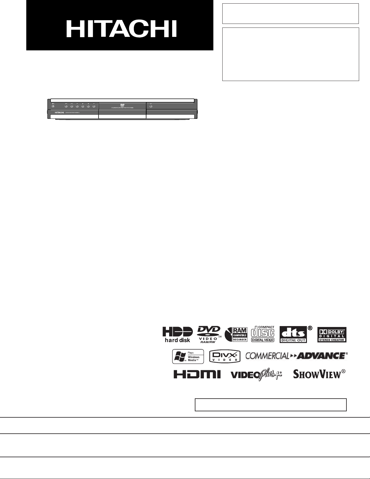
SERVICE MANUAL
SM1515
DV-DS251E
DV-DS161E
DV-DS161EUK
DV-DS81E
DV-DS81EUK
DO NOT RESELL OR DIVERT IMPROPERLY
SPECIFICATIONS AND PARTS ARE SUBJECT TO CHANGE FOR IMPROVEMENT
HDD/DVD RECORDER
2005September
Digital Media Division, YOKOHAMA
Page 2

Table of Contents
1 Safety Precaution for Repair ........... 1-1
1-1 Cautions ................................................. 1-1
1-2 Electrostatic Protection Measures .......... 1-2
1-3 Cautions When Handling DVD Drive....... 1-2
1-4 Cautions When Handling HDD ............... 1-3
1-5 Lead-Free Solder.................................... 1-4
1-6 Notes When Using Service Manual ........ 1-5
2 General Description ......................... 2-1
2-1 Overview ................................................ 2-1
2-1-1 Service method ................................... 2-1
2-1-2 Disc information ................................... 2-2
2-2 Specifications ......................................... 2-4
2-3 Major Differences from Previous Model .. 2-5
2-4 Function Differences from
Previous Model ....................................... 2-6
2-5 Names of Parts....................................... 2-7
2-6 HDMI Connection .................................. 2-10
2-7 List of Abbreviations and Terms for DVD
Recorder ............................................... 2-11
3 Details of Servicing and
Troubleshooting ............................... 3-1
3-1 How to Remove Disc from Faulty
Recorder ................................................ 3-1
3-1-1
Removing Disc without Opening Case.
3-1-2 Removing Disc from Faulty Recorder .. 3-2
3-2 Details of Servicing ................................. 3-2
3-2-1 Setting to defaults at the factory .......... 3-2
3-2-2 Troubleshooting HDD .......................... 3-3
3-2-3 Firmware ............................................. 3-4
(1) Version check procedure .......................... 3-4
(2) Main firmware updating procedure ........... 3-5
(3) Loader firmware updating procedure ........ 3-6
(4) Main/Loader firmware simultaneous
updating procedure................................... 3-6
3-3 Troubleshooting ...................................... 3-7
3-3-1 Troubleshooting electronic system....... 3-7
3-1
4 Disassembly and Reassembly ........ 4-1
4-1 Order of Disassembly ............................. 4-1
4-2 Disassembly ........................................... 4-1
(1) Top Cover ................................................. 4-1
(2) Front Panel ............................................... 4-2
(3) TIMER P.C.B, KEY P.C.B .......................... 4-2
(4) SMPS P.C.B ............................................. 4-3
(5) JACK P.C.B .............................................. 4-3
(6) HDD Unit .................................................. 4-4
(7) CARD P.C.B ............................................. 4-5
(8) MAIN P.C.B, PCB Frame .......................... 4-5
(9) I/O P.C.B, Rear Panel, FAN Motor ............ 4-6
(10) DVD Multi Drive ...................................... 4-7
5 Exploded View and Parts List.......... 5-1
5-1 Exploded View ........................................ 5-1
S Schematic, Wiring Diagrams .......... S-1
S-1 Wiring Diagram .......................................S-1
S-2 SMPS Schematic Diagram ..................... S-2
S-3
SYSTEM Schematic Diagram(I/O P.C.B) ...
S-4
TUNER/JACK Schematic Diagram
(
I/O
P.C.B) ..................................................
S-5 COMMERCIAL ADVANCE Schematic
Diagram(
S-6 JACK Schematic Diagram ...................... S-6
S-7 TIMER,KEY Schematic Diagrams .......... S-7
S-8 CARD-1 Schematic Diagram
(
CARD
S-9 CARD-2 Schematic Diagram
(
CARD
S-10 Circuit Waveforms ............................... S-10
S-11 Circuit Voltage Chart ........................... S-11
I/O
P.C.B) .................................S-5
P.C.B).......................................... S-8
P.C.B).......................................... S-9
S-3
S-4
C Circuit Board Diagrams .................. C-1
C-1 I/O Circuit Board Diagram ...................... C-1
C-2 SMPS Circuit Board Diagram ................ C-2
C-3 JACK Circuit Board Diagram ................. C-2
C-4 LOADER Circuit Board Diagram ............ C-2
C-5 HDD Circuit Board Diagram ................... C-2
C-6 TIMER Circuit Board Diagram ............... C-3
C-7 KEY Circuit Board Diagram ................... C-3
C-8 CARD Circuit Board Diagram ................ C-3
Contents - 1
Page 3

B Block Diagrams ............................... B-1
B-1 Overall Block Diagram ............................ B-1
B-2 SMPS Circuit Block Diagram ..................B-2
B-3 POWER(I/O Board) Circuit Block
Diagram..................................................B-3
B-4 AUDIO/VIDEO Circuit Block Diagram ..... B-4
B-5 SYSTEM Circuit Block Diagram.............. B-5
B-6 COMMERCIAL ADVANCE Circuit Block
Diagram..................................................B-6
Contents - 2
Page 4
1
Safety Precaution for Repair
1-1 Cautions
PRODUCT SAFETY NOTICE
Many electrical and mechanical parts have special safety-related characteristics. These are often not
evident from visual inspection nor can the protection afforded by them necessarily be obtained by using
replacement components rated for a higher voltage, wattage, etc. Replacement parts which have these
special safety characteristics are identified in this Service Manual. Electrical components having such
features are identified by marking with a on the schematics and the parts list in this Service Manual.
The use of a substitute replacement component which does not have the same safety characteristics as
the HITACHI recommended replacement one, shown in the parts list in this Service Manual, may create
shock, fire, or other hazards. Product safety is continuously under review and new instructions are
issued from time to time. For the latest information, always consult the current HITACHI Service Manual.
A subscription to, or additional copies for, HITACHI Service Manual may be obtained at a nominal
charge from HITACHI SALES CORPORATION.
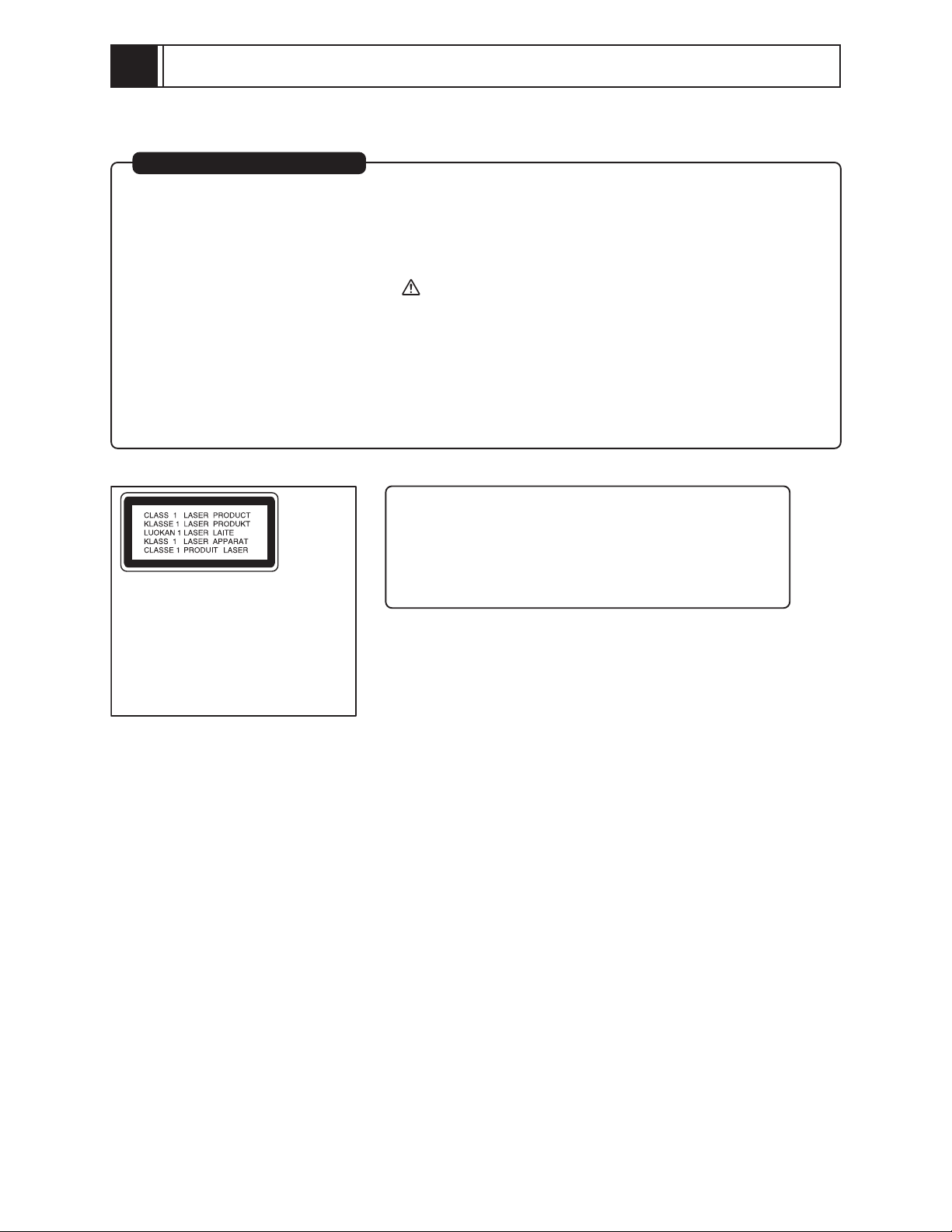
CAUTION
There is a high-voltage section inside the DVD video
recorder. When repairing or inspecting it, take great care
to prevent electric shock: Use an isolating transformer,
CAUTION
This product contains a laser diode of
higher class than 1. To ensure continued safety, do not remove any covers
or attempt to gain access to the inside of the product. Refer all servicing
to qualified personnel.
wear gloves, etc.
1 - 1
Page 5
Safety Precaution for Repair > Electrostatic Protection Measures / Cautions When Handling DVD Drive
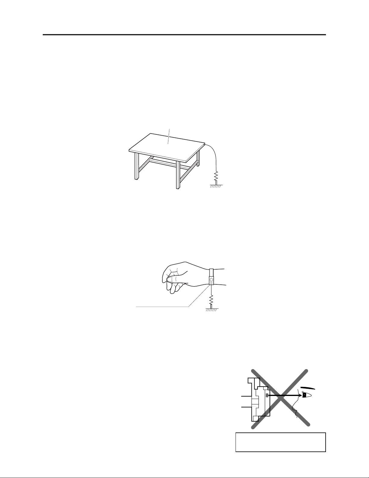
1-2 Electrostatic Protection Measures
Semiconductor components can be damaged by static electricity charged on clothes, human body,
etc. Take great care when handling components to avoid electrostatic damage, and perform
servicing in an environment where grounding is complete.
(1) Grounding work bench
Lay out an antistatic mat on work bench, and then use the ground plate to ground the work bench.
Antistatic mat
1M ohm
Ground
(2) Grounding human body
Use an antistatic wrist strap to discharge any static electricity charged on the body. Also, use a
tester for wrist strap to make sure that the wrist strap is working normally. Note, however, that
static electricity charged on clothes will not be discharged by wrist strap: Therefore do not allow
your clothes to touch the semiconductor components.
Antistatic wrist strap
1M ohm
1-3 Cautions When Handling DVD Drive
The optical pickup in DVD drive has a high precision structure: Be sure to observe the following
cautions.
1) Do not subject optical pickups to any severe vibrations or
impact during movement, installation or disassembly.
2) When performing repair work, do not perform disassembly
any further than that described in this manual.
3) Never turn the semi-variable resistors for adjustment in
optical pickup or DVD drive.
4) NEVER look into the objective lens in optical pickup or
directly view the laser light: You could lose your eyesight.
Do not directly look at laser light
from pickup.
1 - 2
Page 6

Safety Precaution for Repair > Cautions When Handling HDD (Hard Disk Drive)
1-4 Cautions When Handling HDD (Hard Disk Drive)
HDD is a high precision device, and is very susceptible to vibrations or impact. Even if HDD
operates normally immediately after it has been subjected to vibrations or impact, a problem may
occur after it is used for a while: When servicing, take great care with the following.
There are two types of HDD: CSS format (head remains on disk regardless of operation status) and
ramp loading format (head moves away from disk during no operation). The impact resistance
characteristics are slightly different for the two. When servicing, observe the following cautions
regardless of the format:
(1) Cautions during unpacking
1) Do not subject the HDD to any impact when placing on desk: The head hitting against the desk
could result in damage.
2) If condensation occurs because of the environment, leave the HDD without being turned on for at
least 3 hours until it adapts to surrounding environment. If the HDD is turned on while the head
is sticking to disk because of condensation, the disk may be damaged.
(2) Cautions during transportation
An HDD is more susceptible to vibrations or impact when it is turned on or operating than during
no operation.
1) Do not move the HDD while it is turned on: If the HDD is subject to any impact while the disk is
rotating, i.e., the head hitting against the disk, breakage could result.
2) Move the HDD approximately 2 minutes (approximately 30 seconds for surveillance system
devices) after turning it off and unplugging its power cord from AC outlet. The disk will still be
rotating by inertia immediately after the HDD is turned off: Subjecting the HDD to movement at
this time could destroy it.
(3) Cautions during operation
1) Do not unplug the power cord from AC outlet during operation: This could damage the data on
HDD. Be sure to turn the HDD off before unplugging the power cord.
2) Do not hit the HDD: The head hitting the disk could result in breakage.
(4) Caution during packing
1) Use the packing material of relevant model: Material superior in impact resistance is used. Using
other packing materials could result in fault.
(5) Cautions when handling unassembled HDD
1) Hold the HDD at both sides so that the circuit board surface is facing below: Holding the HDD at
the top and bottom could cause the head to drift, which could result in fault.
2) Do not touch the terminal or pattern on circuit board.
3) Place HDD on a spot where cushion is pasted with the circuit board surface facing below.
4) Do not hold or place stacked HDDs.
5) Do not drop or hit HDD against anything: Dropping HDD from even 5 mm high on a work bench
with high stiffness could cause fault.
1 - 3
Page 7
Safety Precaution for Repair > Lead-Free Solder
1-5 Lead-Free Solder
The printed circuit board that uses lead-free solder is adopted. To protect the global environment,
use the recommended lead-free solder also during servicing.
Read and observe the following before soldering:
Caution
ALWAYS wear protective goggles during soldering so that no solder smoke or scattered solder
enters the eye. Lead-free solder may scatter at high temperatures of 600°C.
(1) Characteristics of lead-free solder
The melting point of lead-free solder is 30-40°C higher than that of lead based solder.
(2) Lead-free solder for servicing
Use the following lead-free solder for servicing:
Recommended lead-free solder and composition of alloy (wt%): Sn-3.0Ag-0.5Cu or equivalent
Information:
For composition of alloy, Sn is tin; Ag is silver; Cu is copper; Bi is bismuth; Pb is lead.
(3) Soldering iron for servicing
The temperature of soldering iron tip must be adjusted according to the points to be soldered: Use
an antistatic soldering iron with thermal control function.
When removing components, take care not to damage any surrounding component or pattern. When
attaching components, observe the heating time in the following table so that the components are
not destroyed by heat.
Tip temperatures for different soldering points:
Point to be soldered
Surface-mounted (chip) parts [other than
those shown below]
Surface-mounted (chip) parts [for DVD
cameras, cellular phones only]
Discrete parts
Chassis, metal shield, etc.
320 ± 30°C
[heating time: less than 5 seconds]
350 ± 10°C
[heating time: less than 3 seconds]
380 ± 30°C
420 ± 30°C
Tip temperature
(4) Cautions when using lead based solder
It is recommended that you use lead-free solder when servicing, but it is also possible to service
using lead based solder. However, if lead based solder is used for servicing, take care with the
following:
1) Before using lead based solder, remove the lead-free solder completely from the point to be
soldered.
2) For additional soldering for repair, set the soldering iron tip temperature for lead-free solder, mix
lead based solder and lead-free solder sufficiently. Do not perform any repair using the bare
soldering iron tip without adding solder, since it will cause secondary failure due to lack of
strength.
1 - 4
Page 8
Safety Precaution for Repair > Notes When Using Service Manual
1-6 Notes When Using Service Manual
(1) Value units used in parts list
Certain symbols are indicated as shown below for value units of resistors, capacitors and coils in
parts list. When you read them, note the following regular indications:
Parts
Resistor
Capacitor
Coil
Indication in list Regular indication
KOHM
UF
PF
UH
MH
.........................................
................................................
................................................
...............................................
..............................................
k
µF
pF
µH
mH
(2) Values in schematic diagrams
The values, dielectric strength (power capacitance) and tolerances of the resistors (excluding
variable resistors) and capacitors are indicated in the schematic diagrams using abbreviations.
Certain symbols are indicated for value units: When you read them note the regular indications in
tables below:
[Resistors] [Capacitors]
Item
Value
Tolerance
Power
capacitance
No indication
..................................................
K
.................................................
M
No indication
(All tolerances other than ±5% are
indicated in schematic diagrams)
No indication
(1/16 W for leadless resistors with no
indication)
All capacitances other than the above
are indicated in schematic diagrams.
Indication
..............................
..............................
..............................
k
M
±5%
1/8W
Item
Value
Dielectric
strength
[Coils]
Item
Value
Indication
No indication
..................................................
P
No indication
(All dielectric strengths other than
50 V are indicated in schematic
diagrams)
..............................
..............................
µF
pF
50V
Indication
...................................................
µ
..................................................
m
µH
mH
1 - 5
Page 9
2
General Description
2-1 Overview
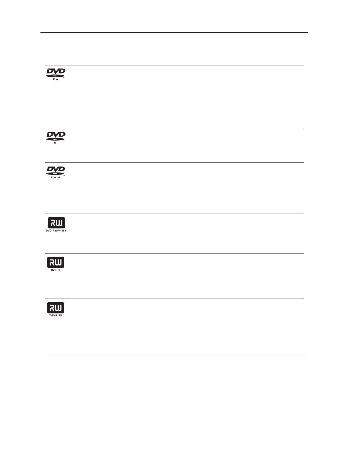
The HDD/DVD recorder models DV-DS251E, DS161E and DS81E all incorporate 250-GB, 160-GB
and 80-GB HDDs, made by Hitachi Global Storage Technologies.
The DVD recorder block contains a DVD multi-drive: It is compatible with recording and playback
of a variety of media – 5x DVD-RAM, 4x DVD-RW, 16x DVD-R, DVD+RW, DVD+R and DVD+R DL.
2-1-1 Service method
Basically, components are replaced when servicing the HDD/DVD recorder. However, the service
method is different for high-density packaging PCBs and precision components.
Refer to the following table and perform the designated, appropriate servicing. Any changes that
occur in the service method will be published using service bulletin, etc.
Do not perform any servicing other than that described in this manual.
Component
Exterior component
DVD Multi Drive
HDD Unit
MAIN P.C.B
I/O P.C.B
SMPS P.C.B
TIMER P.C.B
JACK P.C.B
KEY P.C.B
CARD P.C.B
Service method
Component replacement
Unit replacement
Unit replacement
Circuit board assembly
replacement
Component replacement
Component replacement
Component replacement
Component replacement
Component replacement
Component replacement
KEY P.C.B
JACK P.C.B
DVD MULTI DRIVE
Fig. 2-1-1 Component Location
TIMER P.C.B
SMPS P.C.B
MAIN P.C.B
I/O P.C.B
HDD UNIT
CARD P.C.B
2 - 1
Page 10
General Description > Overview
2-1-2 Disc information
Recordable and Playable Discs
DVD-RW
•DVD-RW discs can be formatted for VR mode recording or Video mode recording.
• These Discs can be recorded on repeatedly. Recordings can be erased, then you can record again
on the same Disc.
[VR mode]
• Recordings can be extensively edited
• Playable only on VR mode compatible players (after finalization)
[Video mode]
• Playable on regular DVD players (after finalization)
• Limited editing features
DVD-R
These Discs can be recorded only once. After you finalize a DVD-R, you cannot record on it or edit it.
•
•DVD-R discs can be only formatted to Video mode.
• Playable on regular DVD players (after finalization).
• Limited editing features
DVD-RAM
•DVD-RAM discs can be formatted for VR mode recording.
These Discs can be recorded on repeatedly. Recordings can be erased, then you can record again on the
•
same Disc.
• Playable on DVD-RAM compatible players.
• Recordings can be extensively edited.
• Only DVD-RAM standard Version 2.0, 2.1 and 2.2 discs can be used in this unit.
• You cannot use the cartridge-type DVD-RAM disc in this unit.
DVD+RW
• These Discs can be recorded on repeatedly. Recordings can be erased, then you can record again
on the same Disc.
• Playable on DVD+RW compatible players (automatically finalization)
• The edited contents are playable on DVD+RW compatible players only after finalization
• Recordings can be edited the title/chapter
DVD+R
• These Discs can be recorded only once. After you finalize a DVD+R, you cannot record on it or edit
it any more.
• Playable on DVD+R compatible players (after finalization)
• Any edited contents are not be compatible on DVD+R compatible players. (Hide, chapter combine,
added chapter mark, etc.)
• Limited title/chapter editing features.
DVD+R DL
• These Discs can be recorded only once. After you finalize a DVD+R DL, you cannot record on it or
edit it any more.
• Storage space is nearly doubled with double layer DVD+R media, allowing consumers to record up
to 8.5GB of video on a single DVD+R DL disc.
• Playable on DVD+R compatible players (after finalization)
• Any edited contents are not be compatible on DVD+R DL compatible players. (Hide, chapter com-
bine, added chapter mark, etc.)
• Limited title/chapter editing features.
2 - 2
Page 11
General Description > Overview
The recordable DVD discs (Example)
DVD-R DVD+R DVD-RW DVD+RW DVD+R (DL) DVD-RAM
Maxell (4x, 8x) Maxell (4x, 8x) Maxell (1x, 2x, 4x) Maxell (2.4x, 4x) Maxell (2.4x) Maxell (3x, 5x)
SONY (8x, 16x) SONY (2.4x, 4x, 8x, 16x) Victor (1x, 4x) TDK (2.4x) Mitsubishi (2.4x) -
TDK (4x, 8x) TDK (4x) TDK (2x) Philips (4x) - -
Verbatim (4x, 8x) Mitsubishi (4x, 8x) Mitsubishi (2x) Ricoh (2.4x) - -
Panasonic (2x, 4x) Ricoh (2x, 4x, 8x) - HP (2.4x, 4x) - -
Note:
If a DVD-RW/DVD+RW disc is recorded using a personal computer or other DVD recorder, you cannot format the
disc using this recorder. So if you want to use the disc on this recorder, you must format the disc using the original recorder.
The above discs were checked for usability in 2005.
Disc specifications may be changed without notice.
Playable Discs
DVD (8 cm / 12 cm disc)
• Discs such as movies that can be purchased or rented
Video CD (VCD) (8 cm / 12 cm disc)
• VIDEO CDs or CD-Rs/CD-RWs in VIDEO CD/Super VIDEO CD format
Audio CD (8 cm / 12 cm disc)
• Music CDs or CD-Rs/CD-RWs in music CD format that can be purchased
CD-R/CD-RW (8 cm / 12 cm disc)
• CD-R/CD-RW discs that contain audio titles, DivX
®
, MP3, WMA, or JPEG files.
Notes:
– Depending on the conditions of the recording equipment or the CD-R/RW (or DVD±R/RW) disc itself, some
CD-R/RW (or DVD±R/RW) discs cannot be played on the unit.
– Do not attach any seal or label to either side (the labeled side or the recorded side) of a disc.
– Do not use irregularly shaped CDs (e.g., heart-shaped or octagonal). Doing so may result in malfunctions.
– Depending on the recording software & the finalization, some recorded discs (CD-R/RW or DVD±R/RW) may
not be playable.
–DVD-R/RW, DVD+R/RW and CD-R/RW discs recorded using a personal computer or a DVD or CD Recorder
may not play if the disc is damaged or dirty, or if there is dirt or condensation on the Recorder’s lens.
– If you record a disc using a personal computer, even if it is recorded in a compatible format, there are cases in
which it may not play because of the settings of the application software used to create the disc. (Check with
the software publisher for more detailed information.)
2 - 3
Page 12

General Description > Specifications
2-2 Specifications
General
Power requirements AC 220-240V, 50/60 Hz
Power consumption 35W
Dimensions (approx.) 432 X 60.5 X 371.5 mm (w x h x d)
Mass (approx.) 5.6 kg
Operating temperature 5˚C to 35˚C
Operating humidity 10 % to 80 %
Television system PAL B/G, SECAM L/L´ colour system [For E]
Recording format PAL
Recording
Recording format DVD Video Recording, DVD-VIDEO
Recordable media HDD, DVD-RW, DVD-R, DVD+RW,
Recordable time DVD (4.7GB): Approx. 1 hour (XP mode), 2 hours (SP mode),
(DVD) 4 hours (LP mode), 6 hours (EP mode)
Recordable time DV-DS251E
(HDD) HDD (250GB): Approx. 66 hours (XP mode), 129 hours (SP mode),
Video recording format
Sampling frequency 27MHz
Compression format MPEG 2 (VBR support)
Audio recording format
Sampling frequency 48kHz
Compression format Dolby Digital
PAL I/II colour system [For E(UK)]
DVD+R, DVD+R (Double Layer),
DVD-RAM
DVD+R DL (8.5GB): Approx. 1 hour 50 minutes (XP mode),
3 hours 40 minutes (SP mode),
7 hours 10 minutes (LP mode), 10 hours 30 minutes (EP mode)
239 hours (LP mode), 356 hours (EP mode)
DV-DS161E/ E(UK)
HDD (160GB): Approx. 48 hours (XP mode), 84 hours (SP mode),
156 hours (LP mode), 233 hours (EP mode)
DV-DS81E/ E(UK)
HDD (80GB): Approx. 21 hours (XP mode), 41 hours (SP mode),
77 hours (LP mode), 114 hours (EP mode)
Playback
Frequency response DVD (PCM 48 kHz): 8 Hz to 20 kHz, CD: 8 Hz to 20 kHz
DVD (PCM 96 kHz): 8 Hz to 44 kHz
Signal-to-noise ratio More than 100 dB (AUDIO OUT connector)
Harmonic distortion Less than 0.008% (AUDIO OUT connector)
Dynamic range More than 95 dB (AUDIO OUT connector)
Inputs
AERIAL IN Aerial input, 75 ohms
VIDEO IN 1.0 Vp-p 75 ohms, sync negative, RCA jack x 2 / SCART x 2
AUDIO IN 0 dBm more than 47 kohms, RCA jack (L, R) x 2 / SCART x 2
DV IN 4 pin (IEEE 1394 standard)
Outputs
VIDEO OUT 1 Vp-p 75 Ω, sync negative, RCA jack x 1 / SCART x 2
COMPONENT VIDEO OUT (Y) 1.0 V (p-p), 75 Ω, negative sync, RCA jack x 1
(Pb)/(Pr) 0.7 V (p-p), 75 Ω, RCA jack x 2
HDMI video/audio output 19 pin (HDMI standard, Type A) (DV-DS251E/161E only)
Audio output (digital audio) 0.5 V (p-p), 75 Ω, RCA jack x 1
Audio output (optical audio) 3 V (p-p), 75 Ω, Optical connector x 1
Audio output (analog audio) 2.0 Vrms (1 KHz, 0 dB), 600 Ω, RCA jack (L, R) x 1 / SCART x 2
• Design and specifications are subject to change without notice.
2 - 4
Page 13
General Description > Major Differences from Previous Model
2-3 Major Differences from Previous Model
Item
Appearance
DV-DS251E/DS161E/DS81E
: Same as on left
DV-RX7000E
PROGRAM
Dimensions
Power consumption
CPRM
Recordable media
Playable media
HDD unit
Remote control
Memory card slot 1 (CF/MD)
Memory card slot 1
(SD/MMC/SMC/xD)
DV input terminal
S-VIDEO input terminal
VIDEO/AUDIO input
terminals
COMPONENT VIDEO
output terminal
S-VIDEO output terminal
VIDEO output terminal
Analog AUDIO output
terminals
Digital AUDIO output
terminals
HDMI terminal
Video output switch
432(W) x 371.5(D) x 60.5(H)mm
Approx. 35 W
Yes
DVD-RAM
DVD-RW
DVD-R
DVD+RW
DVD+R
DVD+R DL
DVD-RAM
DVD-RW
DVD-R
DVD+RW
DVD+R
DVD+R DL
DVD-VIDEO
Video CD (VCD)
Audio CD (CD-DA)
CD-R/CD-RW
(CD-DA, DivX, MP3, WMA, JPEG
formatted discs)
250GB: DV-DS251E
160GB: DV-DS161E/E(UK)
80GB: DV-DS81E/E(UK)
DV-RM251E: For E
DV-RM251E(UK) : For UK
Yes (DV-DS251E, 161E/E(UK) only)
Yes (DV-DS251E, 161E/E(UK) only)
1 (IEEE 1394)
1 (Mini DIN 4pin)
4 (RCA: 2, SCART: 2)
1 (RCA)
--3 (RCA: 1, SCART: 2)
3 (RCA: 1, SCART: 2)
2 (Optical: 1, Coaxial: 1)
1 (DV-DS251E, 161E only)
Yes (COMPONENT-RGB)
430(W) x 279(D) x 69(H)mm
---
---
---
---
---
---
CD-R/CD-RW
(CD-DA, MP3,JPEG formatted discs)
---
---
---
DV-RM7000E
---
---
2 (Mini DIN 4pin: 2)
4 (RCA: 2, SCART: 2)
---
1 (Mini DIN 4pin)
3 (RCA: 1, SCART: 2)
4 (RCA: 2, SCART: 2)
---
Yes (SETUP screen)
2 - 5
Page 14
General Description > Function Differences from Previous Model
2-4 Function Differences from Previous Model
Recording
Dubbing
Tittle List
Playback
Item
Time Shift
Clip Recording
Instant Timer Recording
Timer Recording
Recording Mode
Recording from DV Input
Dubbing (HDD to DVD)
Dubbing (DVD to HDD)
One Touch Copy (HDD to DVD)
Adding Chapter Markers
Changing Title Thumbnails
Making a New Playlist
Adding Title/Chapters
Deleting Title/Chapter
Deleting a Part
Time Search
Sort
Combining Titles
Divide
Combining Chapters
Moving a Playlist Chapter
Hide a Chapter/Title
Protect a Title
Displaying Disc Information
Commercial Advance (CM Skip)
Random
Repeat A-B
Time Search
Zoom
Marker Search
Manual Skip
DivX Movie File Playback
Audio CD Playback
MP3 Playback
WMA file Playback
JPEG File Viewing
P in P
DV-DS251E/DS161E/DS81E
Yes[HDD]
Yes
Yes
Yes
XP, SP, LP, EP, FR
Yes
Yes
Yes
Yes
Yes
Yes
Yes
Yes
Yes
Yes
Yes
Yes
Yes
Yes
Yes
Yes
Yes
Yes
Yes
Yes
Yes
Yes
Yes
Yes
Yes
Yes (15 sec)
Yes
Yes
Yes
Yes
Yes
No
Yes (Time Slip) [DVD-RAM]
One Touch Recording (OTR)
: Same as on left
DV-RX7000E
No
XP, SP, LP, EP, FR
No
No
No
No
No
No
No
No
Yes
No
Yes (15, 30, 60 sec)
No
Yes
Yes
No
Yes
2 - 6
Page 15
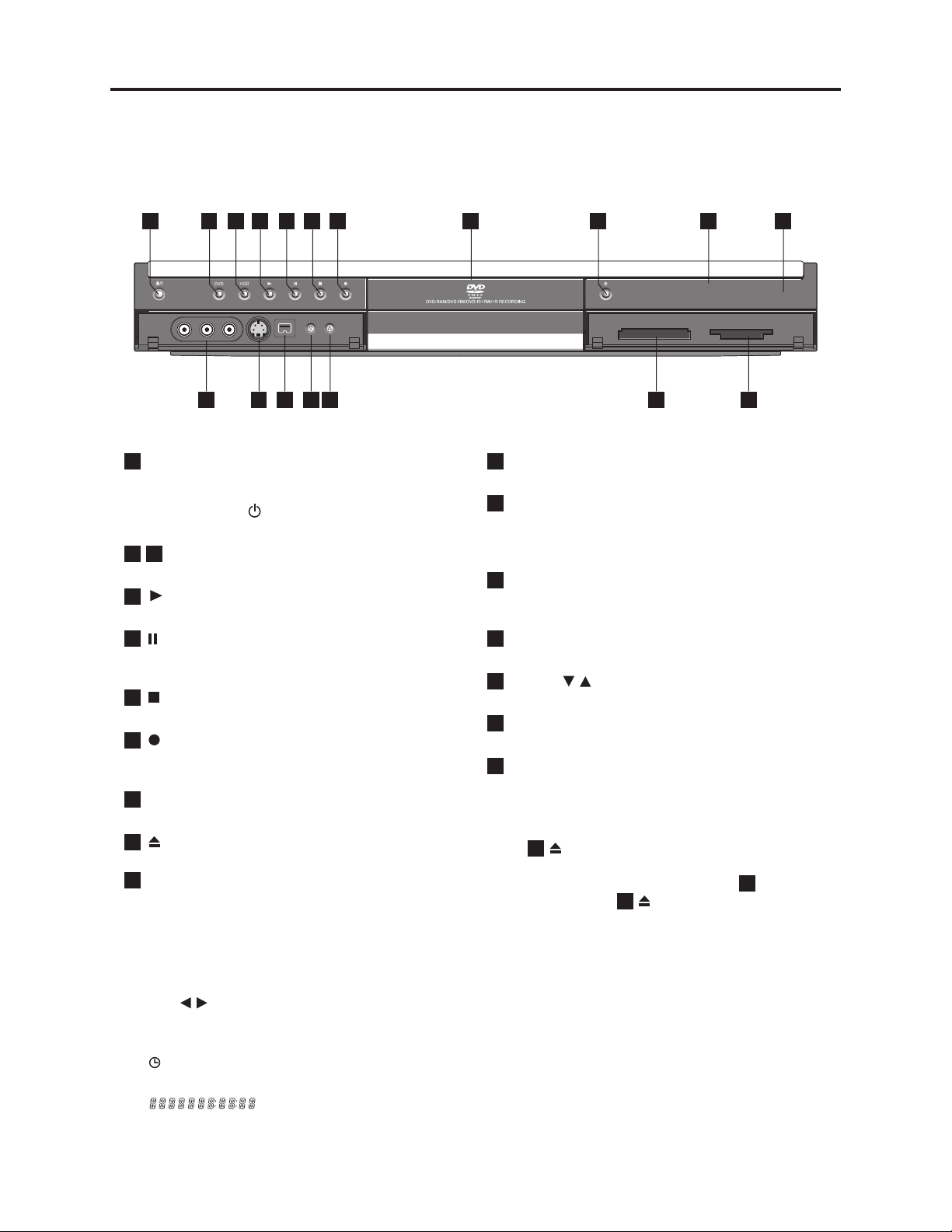
General Description > Names of Parts
2-5 Names of Parts
Front Panel
1
POWER button
1 11
Switches the recorder ON or OFF.
(As to the indication of the Operate switch, “
shows ON and “ ” shows electrical power
stand-by.)
2
3
Set the recorder’s mode to DVD or HDD.
4
Starts playback.
5
Pause playback or recording temporarily, press
again to exit pause mode.
6
Stops playback or recording.
7
Starts recording. Press repeatedly to set the
recording time.
Disc Tray
8
Insert a disc here.
9
Opens or closes the disc tray.
10
Display window
Shows the current status of the recorder.
T/S: Indicates the timeshifting mode.
REC: The recorder is recording.
HDD: The recorder is HDD mode.
DVD: The recorder is DVD mode.
HDD DVD: The recorder is dubbing.
TV: Indicates when the recorder is in TV tuner
mode.
ing or a timer recording is programmed.
time, elapsed time, title number, chapter/track
number, channel, etc.
2 3 4 5 6 7 8 9 10 11
12 13 14 15 15 16 17
I
”
DVD/HDD
(PLAY)
(PAUSE/STEP)
(STOP)
(REC)
(OPEN/CLOSE)
: Indicates when the recorder is in timer record-
: Indicates clock, total playing
Remote Sensor
Point the recorder remote control here.
INPUT4 (VIDEO IN/AUDIO IN (Left/Right))
12
Connect the audio/video output of an external
source (Audio system, TV/ Monitor, VCR,
Camcorder, etc.).
INPUT 4 (S-VIDEO IN)
13
Connect the S-Video output of an external source
(TV/ Monitor, VCR, Camcorder, etc.).
14
DV IN
Connect the DV output of a digital camcorder.
PROG. ( / )
15
Scans up or down through memorized channels.
16
MEMORY CARD Slot 1 (DV-DS251E/161E/161E
(UK) only) Insert a memory card (CF/MD).
17
MEMORY CARD Slot 2 (DV-DS251E/161E/161E
(UK) only) Insert a memory card (SD/MMC/SMC
/xD).
Note:
• The (OPEN/CLOSE) button will not operate
9
with this recorder turned off. After turning the
recorder on to display the clock in the Display
window, press the (OPEN/CLOSE) button.
9
10
2 - 7
Page 16
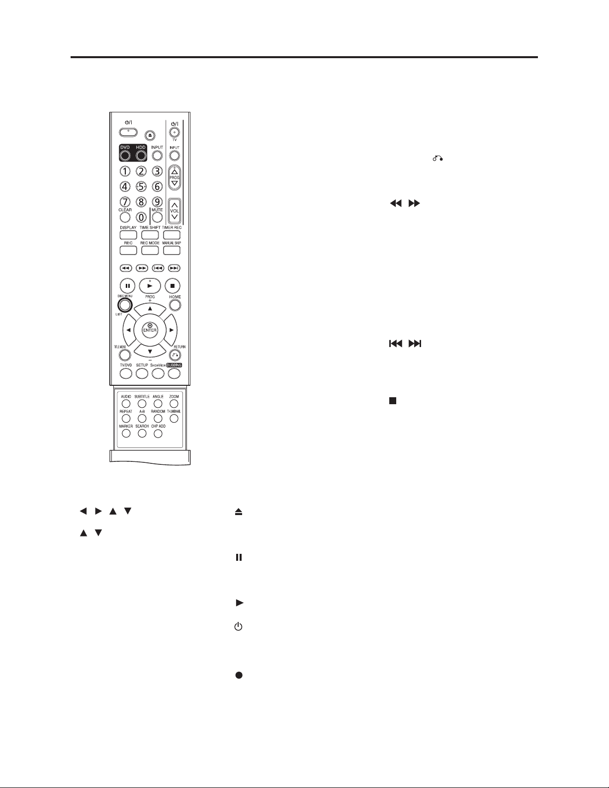
General Description > Names of Parts
Remote Control
0-9 numerical buttons:
Selects numbered options in a
menu.
/ / / (left/right/up/down):
Selects an option in the menu.
/ (up/down): Scans up or
down through memorized channels.
A-B: Repeat sequence.
ANGLE: Selects a DVD camera
angle, if available.
AUDIO: Selects an audio
language (DVD) or TV audio
channel (CD).
CHP ADD:
Inserts a chapter marker when
playing/recording.
CLEAR: Removes a track number
on the Program List or a mark on
the Marker Search menu.
DISC MENU/LIST:
Accesses menu on a DVD disc.
Switches between Title ListOriginal and Title List-Playlist
menu.
DISPLAY:
Accesses On-Screen Display.
DUBBING: Copies DVD to HDD
(or HDD to DVD).
DVD: Select the Recorder’s
function mode to DVD.
ENTER
- Acknowledges menu selection.
- Displays information while view-
ing a TV program.
HDD: Select the Recorder’s
function mode to HDD.
HOME: Accesses or removes the
HOME menu.
INPUT: Changes the input to use
for recording (Tuner, AV1-4 or DV
IN).
MANUAL SKIP:
Pressing this button during playback will skip to a scene 15 seconds forward.
MARKER:
playback.
(OPEN/CLOSE):
Opens and closes the disc tray.
Operate this button only after turning the recorder on.
(PAUSE/STEP):
Pause playback or recording temporarily, press again to exit pause
mode.
(PLAY):
Starts play-back.
/ I POWER:
Switches the recorder ON or OFF.
RANDOM:
Plays tracks in random order.
(REC): Starts recording.
Press repeatedly to set the
recording time.
Marks any point during
REC MODE: Selects the recording
mode (XP, SP, LP or EP).
REPEAT:
Repeat chapter, track, title, all.
RETURN ( )
- Removes the menu.
- Display the menu of a video CD
with PBC.
/ (SCAN):
Search backward or forward.
SEARCH:
Displays Marker Search menu.
SETUP:
the Setup menu.
S
HOWVIEW
program menu for S
System programming.
VIDEO Plus+ : (For UK)
To display the program menu for
VIDEO Plus+ System programming.
Go to next chapter or track.
Returns to beginning of current
chapter or track or go to previous
chapter or track.
Stops playback or recording.
SUBTITLE:
Selects a subtitle language.
THUMBNAIL: Selects a thumbnail
picture for the current title and
chapter for use in the Original and
Playlist menu.
TIMER REC:
Displays Timer Record menu.
TIMESHIFT: Activates pause live
TV/playback (timeshift) for a live
TV program.
TITLE MENU:
Displays the disc’s Title menu, if
available.
TV/DVD: To view channels
selected by the recorder tuner or
by the TV tuner.
TV Control Buttons
- POWER: Turns the TV on or off.
-INPUT: Selects the TV’s source.
- PROG +/–: Selects TV’s chan-
- VOL +/–: Adjusts TV’s volume.
- MUTE: Temporarily turns TV
ZOOM:
Enlarges DVD video image.
Accesses or removes
: To display the
HOWVIEW
/ (SKIP):
(STOP):
nel.
sound OFF, press again to
restore.
2 - 8
Page 17
General Description > Names of Parts
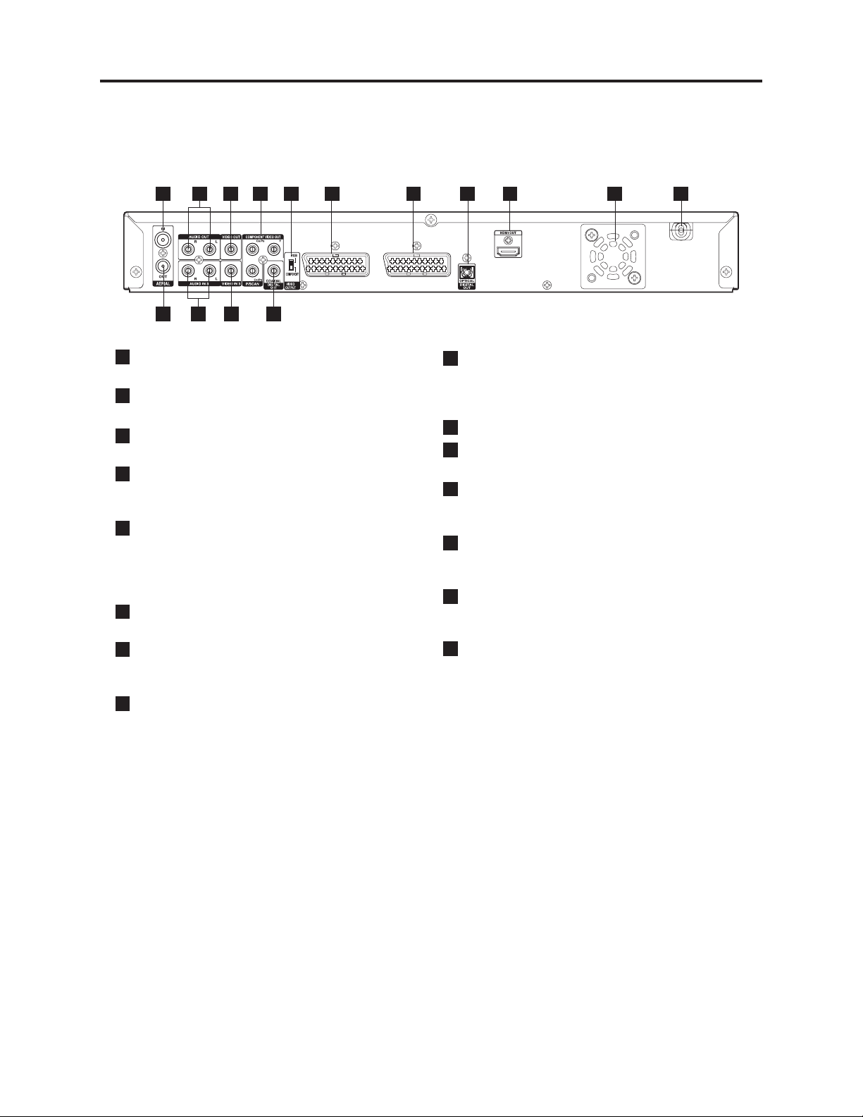
Rear Panel
1
2 3 4 5 6 7 8 9 10 11
12 13 14 15
1
AERIAL
Connect the aerial to this terminal.
2
AUDIO OUT (Left/Right)
Connect to a TV with audio inputs.
VIDEO OUT
3
Connect to a TV with video inputs.
4
COMPONENT VIDEO OUT/PROGRESSIVE
SCAN (Y Pb Pr)
Connect to a TV with Y Pb Pr inputs.
VIDEO OUTPUT Switch
5
Select either COMPONENT VIDEO OUT or RGB
signal of EURO AV1 AUDIO/VIDEO terminal
depending on how you connect the recorder to the
TV.
6
EURO AV 1 AUDIO/VIDEO
Connect to a TV with SCART jack.
7
EURO AV 2 DECODER
Connect the audio/video output of an external
source (Pay-TV decoder, Set Top Box, VCR, etc.).
HDMI Connector (Type A)
9
(DV-DS251E/161E only)
HDMI output providing a high quality interface for
digital audio and video.
10
Cooling fan
11
AC Power Cord
Plug into the power source.
RF. OUT
12
Passes the signal from the AERIAL to your
TV/monitor
AUDIO IN 3 (Left/Right)
13
Connect the audio output of an external source
(Audio system, TV/Monitor, VCR, Camcorder).
VIDEO IN 3
14
Connect the video output of an external source
(Audio system, TV/Monitor, VCR, Camcorder).
15
COAXIAL (Digital audio out jack)
Connect to digital (coaxial) audio equipment.
8
OPTICAL (Digital audio out jack)
Connect to digital (optical) audio equipment.
2 - 9
Page 18
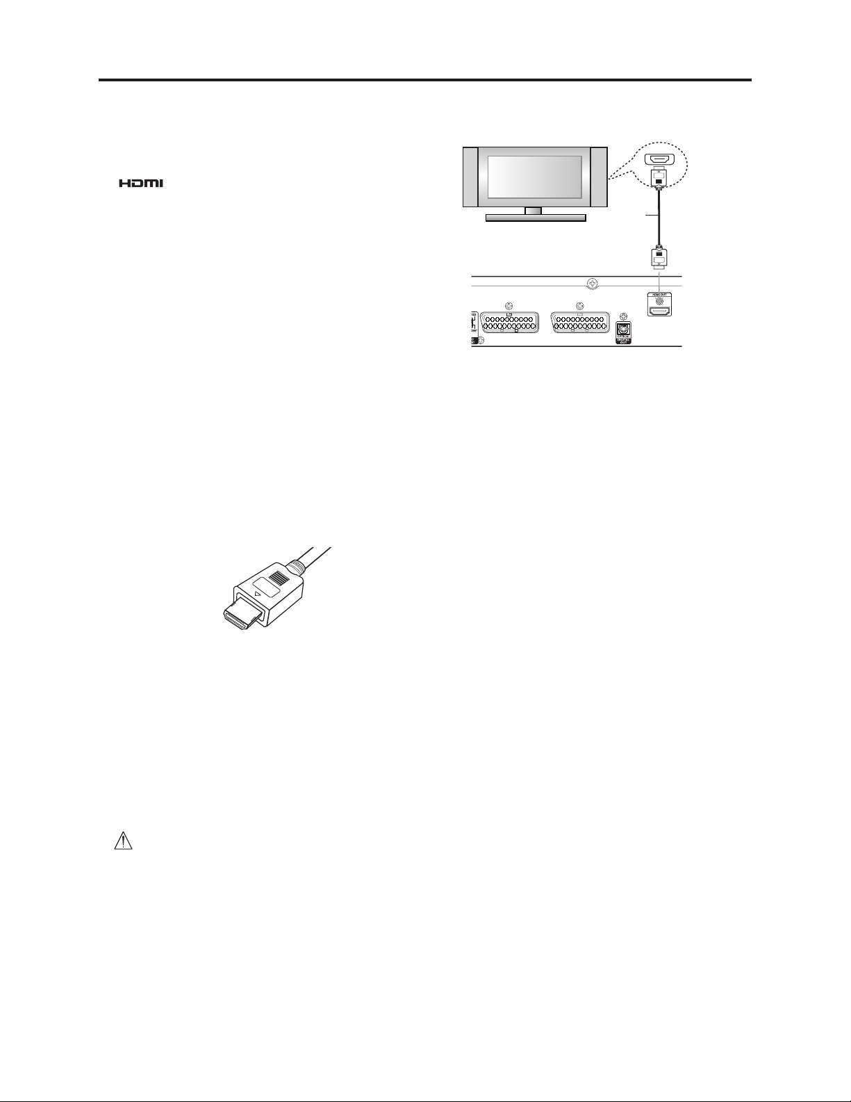
General Description > HDMI Connection
2-6 HDMI Connection (DV-DS251E/DS161E only)
If you have a HDMI TV or monitor, you can connect it
to this recorder using a HDMI cable.
Be sure to use an HDMI cable with HDMI logo
().
1. Connect the HDMI jack on the recorder to the
HDMI jack on a HDMI compatible TV or monitor
(H).
2. Set the TV’s source to HDMI (refer to TV’s Owner’s
manual).
Notes:
• When you use the HDMI connection, the audio’s
sampling frequency is outputted only with 48kHz
even if you select [96kHz].
• This recorder does not perform internal (2 channel)
decoding of a DTS sound track. To enjoy DTS
multi channel surround, you must connect this
recorder to a DTS compatible receiver via one of
this recorder’s digital audio outputs.
• No sound will be outputted from HDMI cable if
the [Dolby Digital] or [MPEG] option is not set to
[PCM] on the Setup menu.
• The arrow on the cable connector body should face
up for correct alignment with the connector on the
recorder.
(Type A)
• If there is noise or lines on the screen, please check
the HDMI cable.
Tip:
When you use HDMI connection, you can change the
resolution (576i, 576p) for the HDMI output by setting
the [Progressive Scan] option in the setup menu.
• Progressive Scan ON mode: 576p
• Progressive Scan OFF mode: 576i
• The recorder does not support 720p and 1080i res-
olutions for HDMI.
Caution
Changing the Progressive Scan mode when the
recorder is connected with HDMI connector may result
in malfunctions. To solve the problem, turn off the
recorder and then turn it on again.
Information on HDMI
Some TVs with HDMI interface do not support "Progre-
ssive Scan OFF mode: 576i". If no image appears when
the HDMI connectors on recorder and TV are joined,
connect the analog VIDEO OUT jack to the video input
on TV, in order to display the image through the recor-
der. Then use the Setup menu on recorder to specify
[Progressive Scan ON mode: 576p].
2 - 10
HDMI compatible TV
Rear of the recorder
About HDMI
HDMI (High Definition Multimedia Interface) supports
both video and audio on a single digital connection for
use with DVD Players, Set-Top Boxes, and other AV
devices.
HDMI was developed to provide the technologies of
HDCP (High-bandwidth Digital Content Protection).
HDCP is used to protect digital content transmitted
and received.
HDMI has the capability to support standard,
enhanced, or high-definition video plus standard to
multi-channel surround-sound audio, HDMI features
include uncompressed digital video, a bandwidth of up
to 5 gigabytes per second, one connector (instead of
several cables and connectors), and communication
between the AV source and AV devices such as
DTVs.
HDMI, the HDMI logo and High-Definition Multimedia
Interface are trademarks or registered trademarks of
HDMI licensing LLC.
Additional Information for HDMI
• When you connect a HDMI or DVI compatible
device make sure of the followings:
-Try switching off the HDMI/DVI device and this
recorder. Next, switch on the HDMI/DVI device
and leave it for around 30 seconds, then switch
on this recorder.
- The connected device’s video input is set correctly
for this unit.
- The connected device is compatible with
720(1440)x576i or 720x576 progressive video
input.
• Not all HDCP-compatible DVI devices will work with
this recorder.
- It’s impossible copy protected-DVD title’s playback
in non-HDCP devices.
• If you select the HDMI output, outputs other than
digital tuner output - such as D1/D2/D3 video outputs, component video outputs, S1 video output and
video output (from yellow jack) - cannot be displayed.
HDMI
H
Page 19
General Description > List of Abbreviations and Terms for DVD Recorder
2-7 List of Abbreviations and Terms for DVD Recorder
Index
A
B
C
D
H
Abbreviation/Term
AC3
Black Level
CPRM
CD-R
CD-RW
Component video
output terminals
Decoder
Dynamic Range
Dolby AC3
DRC
DTS
DVD
DVD-Audio
DVD-R
DVD-RAM
DVD-RW
DVD-Video
DVD Video Format
DVD Video
Recording Format
HDMI
Explanation
See Dolby AC3.
Function to correct the gradations on dark portions to make dark scenes easierto-see.
Content Protection for Recordable Media: Copyright protection function that is
suitable for online distribution of music.
One type of DVD standard disc, to which writing once is possible (recordable
type)
One type of CD standard disc, to which writing up to 1000 times is possible
Used for outputs of HDTV video signal format. Since signals for brightness and
colors are independently handled for components signals (Y: luminance signal;
PR/PB: chrominance signals), degrading of image will be reduced.
A device that decodes the data coded and recorded on DVD Video and restores it
to video and audio signals. This processing is referred to as decoding.
A difference between maximum and minimum levels of audio recorded on disc:
Measured in decibel (dB) units. If the dynamic range is compressed (audio DRC),
the minimum signal level will increase and the maximum signal level will
decrease: This will reduce the higher audio signal - such as burst sound - so that
the low-level audio signal - such as human voice - can be heard more clearly.
Audio coding format developed by Dolby Laboratories in U.S, also simply
referred as AC3 format: Supports 5-channel full-range sound and one channel
for sub-woofer sound playback.
Dynamic Range Control: Adjusting the audio range of maximum and minimum
levels (dynamic range) will improve audio signal when, for example, dialog is
hard to hear or user is watching movies late at night.
Digital Theater System: Sound system as for movie theaters developed by US
Digital Theater Systems, Inc. The number of channels provided by DTS is the
same for Dolby AC3.
Digital Versatile Disc. A huge amount of digital data for video (movie) and audio
can be recorded on this disc, whose size is the same as CD.
One type of DVD standard disc, on which high-quality audio can be recorded
One type of DVD standard disc, to which writing once is possible (recordable
type)
One type of DVD standard disc, to which writing up to 100,000 times is possible
One type of DVD standard disc, to which writing up to 1000 times is possible
One type of DVD standard disc, on which high-quality video and audio can be
recorded
Video recording/playback standard that applies to DVD-Video, DVD-R and DVDRW
Video recording/playback standard that applies to DVD-RAM and DVD-RW:
This allows versatile editing functions, differing from the DVD Video Format.
High-Definition Multimedia Interface: A digital video/audio input/output
interface standard, mainly applied to home electronics and AV devices.
The specifications of DVI (Digital Visual Interface), the display connection
technology, were compiled for AV devices.
Although multiple cables for video, audio and control signals were previously
necessary to connect devices, only one cable is needed with HDMI.
2 - 11
Page 20

General Description > List of Abbreviations and Terms for DVD Recorder
Index
I
J
M
O
P
S
W
Num.
Abbreviation/Term
I/P/B
JPEG
MPEG
MPEG Audio Layer
2
MP3
Optical digital
audio output
Pan & Scan/
Letterbox
Playback Control
(PBC)
Progressive
playback function
S-Video Output
Sampling
Frequency
WMA
3D surround
Explanation
DVD recorders normally use data that is common between images, and
individually record different data for each image.
I-picture: Images recorded independently for the reference of commonly used
data.
P-picture: Images created from past I-picture or P-picture
B-picture: Images created from both I and P pictures, which interact between
both types
Since I-picture delivers the highest image quality, selecting I-picture is
recommended when adjusting image quality.
Joint Photographic Expert Group: International standard format for
compressing still images.
Moving Picture Experts Group: Standard related to compression of digital video
and audio. MPEG2 is a higher standard of MPEG and is applied to video (movie)
requiring higher quality.
One of three audio compression standards (layers 1-3) defined by MPEG
MPEG1 Audio Layer-3: Audio data digital compression technology.
Audio is usually converted to an electrical signal and transmitted from DVD to a
device such as amp: When audio is converted to a digital signal, this optical
digital audio output can be transmitted on optical fiber.
Most DVD videos are produced assuming that they will be displayed on wide TV
screen (aspect ratio of 16:9): If they are displayed on TV screens with 4:3 aspect
ratio, 16:9 images will not quite fit on 4:3 screens. There are two ways of
displaying 16:9 images on 4:3 TV:
· Pan & Scan: Cuts out the left and right ends of images and displays them on
whole screen.
· Letterbox: Reproduces 16:9 images on 4:3 screens with black bands across the
top and bottom of screen.
One format to play Video CD: User can select desired screens and data while
watching the displayed menu screen.
This function converts interlaced images to non-interlaced images and displays
them. It can play back 24-frame/second images included in DVD movie software,
etc.
The video signal is separated into chrominance (C) and luminance (L) signals
and transmitted to TV: This delivers clearer images.
Sampling slices audio waves (analog signal) at a specified time interval, and
digitizes the levels of the sliced waves. The slicing number per second is referred
to as the sampling frequency: The higher the number, the closer the sound to
the original.
Windows Media Audio: Codec that was developed by Microsoft Corporation in
USA.
This technology localizes sound at any position using only two front speakers, by
subjecting the L and R signals to matrix operation. It uses the four transfer
functions from L/R speakers located at specified positions to both ears of listener
located in a specified position, taking into account the shape of head and the
effect of earlobes, and the two transfer functions from any position to both ears.
2 - 12
Page 21

3
Details of Servicing and Troubleshooting
3-1 How to Remove Disc from Faulty Recorder
3-1-1 Removing Disc without Opening Case
1) Open the DVD door of disc tray block by hand; paste plastic tape onto the DVD door, and pull the
tape: The door will easily open.
2) Insert a pin (unbended clip, etc.) into the hole shown in the detailed diagram of pin insertion
location in Fig. 3-1-1.
3) Push in the pin with reasonable force: The disc tray will come out slightly.
Detailed diagram of pin insertion location
Disc tray
(If it is inserted horizontally, it will
Eject
mechanism
not reach the eject mechanism
since it is caught midway.)
Sectional view of pin
insertion hole portion
Fig. 3-1-1 Removing Disc (1)
4) Hold both edges of disc tray with fingers, and pull the tray out little by little to remove the disc.
Fig. 3-1-2 Removing Disc (2)
3 - 1
Page 22

Details of Servicing and Troubleshooting > Details of Servicing
3-1-2 Removing Disc from Faulty Recorder
If disc cannot be removed due to fault, disassemble the recorder and remove the disc by the
following procedure:
1) Remove the top cover.
[See 4-2 (1) for removal procedure.]
2) Remove the front panel.
[See 4-2 (2) for removal procedure.]
3) Push the white component portion under the
disc tray strongly, and the tray will come
slightly forward.
Remove the disc tray in the direction of arrow.
Perform this work carefully, making sure that
the disc is not scratched.
DISC TRAY
Fig. 3-1-3 Removing Disc (3)
DVD MULTI DRIVE
PIN
3-2 Details of Servicing
3-2-1 Setting to defaults at the factory
Perform the following procedure to reset this HDD/DVD recorder to the
initial status when it was shipped from the factory (defaults):
1) Press the SETUP button on remote control and use the cursor
buttons to choose the [Initialization] menu.
2) Press the cursor button to move to the second level.
3) Use the cursor buttons to choose “Factory Set”, and then press
the ENTER button.
The confirm message will appear.
4) Use the cursor buttons to select [Yes], and then press the ENTER
button.
Prov.
GENERAL
Auto Programming
Program Edit
Clock Set
TV Aspect
Display Mode
Progressive Scan
PBC
Initialization
Move
Fig. 3-2-1
Factory Set
HDD Format
M/C Format
Enter
3 - 2
Page 23

Details of Servicing and Troubleshooting > Judging Faults in HDD
3-2-2 Troubleshooting HDD
This section shows how to determine a fault in HDD and how to format a new HDD to replace the
faulty HDD.
(1) HDD troubleshooting method
If the playback picture temporarily stops or distortion occurs frequently, the HDD may be faulty. If
this happens, observe the defective phenomenon, decide whether the HDD is faulty, and then repair
or replace the HDD.
When replacing the HDD, note that the data on the old HDD cannot be transferred to a new HDD.
Information:
When discarding a faulty HDD, physically destroy it or perform procedure as required, according to
the regulations in each country, in order to protect any personal information.
Diagnosis using HDD operation sound
Remove the top cover, and check the
operation sound of HDD unit.
Is one click heard
from HDD when power
is turned on?
Yes
Is one click heard
from HDD when power
is turned off?
Yes
Is any operation
sound heard in cases other
than above?
Yes
HDD is faulty.
Replace it and recheck.
No
No
No
Recorder stops at the same
point during HDD playback.
HDD is faulty.
Replace it and recheck.
HDD is faulty.
Replace it and recheck.
HDD is normal.
does not disappear from front display.
"PLEASE WAIT"
Does the phenomenon
disappear when the
HDD is replaced?
No
Re-place the original HDD.
Does the phenomenon
disappear when the
HDD drive is replaced?
No
Re-place the original HDD drive.
Does the phenomenon
disappear when the
Main PCB is replaced?
No
Check the power system.
Yes
Yes
Yes
Recorder stops at the same
point during HDD recording.
HDD is faulty.
HDD drive is faulty.
Main PCB is faulty.
Ask customer whether the recorded contents
can be erased, and acquire approval.
Initialize the HDD,
and perform recording and playback.
Does playback stop at the
same recorded point?
Yes
HDD is probably faulty.
Replace the HDD and recheck.
HDD is normal.
No
(The PCB may be faulty.)
3 - 3
Ask customer whether the recorded contents
can be erased, and acquire approval.
Initialize the HDD, and perform recording.
Does recording stop
at the same point?
Yes
HDD is probably faulty.
Replace the HDD and recheck.
No
HDD is normal.
(The PCB may be faulty.)
Page 24

Details of Servicing and Troubleshooting > Judging Faults in HDD
(2) Formatting HDD
After replacing the built-in HDD, use the following procedure to format
the new HDD:
Prov.
GENERAL
Auto Programming
Program Edit
Clock Set
TV Aspect
Display Mode
Progressive Scan
PBC
Initialization
Move
Factory Set
HDD Format
M/C Format
Enter
1) Press the SETUP button on remote control and use the cursor
buttons to choose the [Initialization] menu.
2) Press the cursor button to move to the second level.
3) Use the cursor buttons to choose “HDD Format” and then press
the ENTER button.
The confirm message will appear.
4) Use the cursor buttons to select [Yes] and then press the ENTER
button.
Fig. 3-2-2
3-2-3 Firmware
The firmware is occasionally updated to improve performance.
Check whether a customer complaint can be solved by updating of firmware. If the complaint can be
solved, update the firmware.
Information:
If any corrections in firmware are made at the factory, information on how to obtain the
firmware data and create a disc containing upgraded firmware will be reported in technical
bulletin, etc.
(1) Version check procedure
1) With the HDD/DVD recorder turned on, make sure that no disc is
inserted.
2) Connect a monitor TV to the video output terminals on this HDD/
DVD recorder.
3) Press the SETUP button on remote control and use the cursor
buttons to choose the [LOCK] menu (Fig. 3-1-4).
4) Press numeric buttons “7” “8” “8” “9” on the remote control in
sequence.
5) The firmware version screen will appear on the monitor TV
(Fig. 3-2-3).
6) Turn the HDD/DVD recorder off to switch off the display.
LOCK
Rating
Set Password
Area Code
DivX Reg. Code
Select
SET: Ver=50914A Cware=prod079 BSP=23 FME
IO: Ver=R42(D47). Loader : T018 MCard : VER 0.10
Select
LOCK
Rating
Set Password
Area Code
DivX Reg. Code
Close
Yes
Close
3 - 4
Fig. 3-2-3
Page 25

Details of Servicing and Troubleshooting > Firmware
(2) Main firmware updating procedure
(2-1) To make Main firmware updating CD
1) Store the Main firmware data in PC.
2) Start a CD writer program, and drag the Main firmware data file (write it to the Root folder on
CD).
3) Check the file name (LG_HDR_UPDATE.004). If it is incorrect, rename it.
4) Change the volume name of CD to RH7000_UP.
5) Write the Main firmware data to a CD-R or CD-RW.
(2-2) To updating the Main firmware
1) Turn the HDD/DVD recorder on and press the OPEN/CLOSE
button.
2) Insert the firmware disc.
3) Press HOME button on the remote control to display the Home Menu
screen (Fig. 3-2-4).
4) Select the [DISC] and press the ENTER button. Options appear.
5) Select the [MOVIE] and press the ENTER button: The screen for
verifying update will appear (Fig. 3-2-5).
6) Select the [YES] and press the ENTER button: The screen for
verifying update will appear (Fig. 3-2-6).
M E D I A
HOME
HDD
DISC
MEMORY CARD
M E D I A
HOME
HDD
DISC
MEMORY CARD
TV(HDD)
MOVIE
MUSIC
PHOTO
Fig. 3-2-4
Firmware Upgrade Start
TV(HDD)
Yes No
MOVIE
MUSIC
PHOTO
7) Press the REC button on this HDD/DVD recorder three times: Both
the current version of main firmware and the version of main
firmware on the disc will appear on the screen (Fig. 3-2-7).
8) Pressing the REC button on this HDD/DVD recorder will start
writing (Fig. 3-2-8).
To cancel writing, press the OPEN/CLOSE button and remove the
disc.
9) When updating is complete, the tray will open automatically: Remove
the disc.
10) Turn the HDD/DVD recorder off and then on: The firmware is now
updated.
Fig. 3-2-5
Run: REC KEY 3 times
Open: Other KEY
Fig. 3-2-6
Current Version
SET : Ver=50912A Cware=prod078 BSP=23
New CD Write Version
SET : Ver=50914A Cware=prod079 BSP=23”
RECKEY:WRITE OPEN:CANCEL
Fig. 3-2-7
Current Version
SET : Ver=50912A Cware=prod078 BSP=23
New CD Write Version
SET : Ver=50914A Cware=prod079 BSP=23”
56 percent ok
3 - 5
Fig. 3-2-8
Page 26

Details of Servicing and Troubleshooting > Firmware
(3) Loader firmware updating procedure
(3-1) To make loader firmware updating CD
1) Store the loader firmware data in PC and decompress it: Three files (prm, bin, bin) will appear.
2) Start a CD writer program and drag the three loader firmware data files (write them to the Root
folder on CD).
3) Change the volume name of CD to DRIVE_UP.
4) Write the loader firmware data to a CD-R or CD-RW.
(3-2) To updating the loader firmware
1) Turn the HDD/DVD recorder on and press the OPEN/CLOSE
button.
2) Insert the firmware disc: The screen for verifying update will appear
(Fig. 3-2-9).
3) Press the REC button on this HDD/DVD recorder three times: The
data on disc will be read, the Firmware Update screen will appear,
and the loader firmware version along with the version of loader
firmware on the disc, will appear on the screen (Fig. 3-2-10).
When reading the data on disc is complete, the disc tray will open
automatically: Remove the disc.
4) Press the REC button on this HDD/DVD recorder.
To cancel writing, press the OPEN/CLOSE button.
5) Turn the HDD/DVD recorder off automatically.
Run: REC KEY 3 times
Open: Other KEY
Fig. 3-2-9
Current Loader Version
DVD+-R/RW : Ver=T018 xx=xxxx
New CD Write Version
DVD+-R/RW : Ver=T019 xx=xxxx
RECKEY:WRITE OPEN:CANCEL
Fig. 3-2-10
(4) Main/Loader firmware simultaneous updating procedure
(4-1) To make firmware updating CD
1) Start a CD writer program, and write the Main and Loader firmware
data to one CD-R or CD-RW in the “Track at once” mode.
(4-2) To update the firmware
1) The method of simultaneously updating the Main/Loader firmware
programs is basically the same as that for updating individual
programs. When the firmware disc is inserted, the screen for
choosing the firmware programs to be updated will appear: Choose
[All] (Fig. 3-2-11).
After the Main firmware is updated, the Loader firmware updating
screen will automatically appear.
==== Firm Ware Update =====
ALLLoaderMain
Fig. 3-2-11
3 - 6
Page 27

Details of Servicing and Troubleshooting > Troubleshooting
3-3 Troubleshooting
3-3-1 Troubleshooting electronic system
(1) SMPS Circuit
Checking power line on I/O PCB
F101: Normal?
YES
BD101: Normal?
YES
R101: Normal?
YES
Is Vcc (10V - 17V)
supplied to IC101 Pin7?
YES
D121: Normal?
YES
IC103 Pin1: Approx. 2.5V? Replace IC103.
NO
NO
NO
NO
NO
NO
Replace F101.
Replace BD101.
Replace R101.
Check D102, and
replace if necessary.
Replace D121.
D127 Anode: Voltage? Replace D127.
YES
D128 Cathode: Voltage?
YES
Power Line on I/O PCB
Shorted.
NO
NO
Replace D128.
YES
D126 Cathode: Voltage? Replace D126.
YES
D130 Cathode: Voltage? Replace D130.
YES
NO
NO
3 - 7
Page 28

Details of Servicing and Troubleshooting > Troubleshooting
Checking power line on MAIN PCB
F101: Normal?
YES
BD101: Normal?
YES
R101: Normal?
YES
Is Vcc (11V - 18V)
supplied to IC104 Pin7?
YES
D122 Cathode: Voltage?
NO
NO
NO
NO
NO
Replace F101.
Replace BD101.
Replace R101.
Check Q111, and
replace if necessary.
Replace D122.
No 5VD
Is 5.4V supplied to
Q120-E?
YES
Is Q126-B: "H"?
YES
Check Q120, and
replace if necessary.
No 12VA
IC156 Pin1: Approx. 14V?
NO
NO
NO
Check D121, and
replace if necessary.
Check the PWR CTL
"H" signal from µ-com
Check D126, and
replace if necessary.
YES
IC106 Pin1: Approx. 2.5V? Replace IC106.
YES
D123 Cathode: Voltage? Replace D123.
YES
D124 Cathode: Voltage? Replace D124.
YES
D125 Cathode: Voltage? Replace D125.
YES
NO
NO
NO
NO
Power Line on Main PCB
Shorted.
YES
IC156 Pin2: Approx. 12V?
YES
Check C153, and
replace if necessary.
No 12V
IC153 Pin1: Approx. 14V?
YES
IC153 Pin4: Approx.
3.3V ~ 5V?
YES
NO
NO
NO
Check IC156, and
replace if necessary.
Check D126, and
replace if necessary.
Check the PWR CTL
"H" signal from µ-com
3 - 8
Check IC153, and
replace if necessary.
Page 29

Details of Servicing and Troubleshooting > Troubleshooting
FL Display does not light.
R107: Normal?
YES
D128 Cathode: Voltage?
YES
ZD151: Normal?
YES
Check D127, and
replace if necessary.
NO
NO
NO
No 3.3V
Check R107, and
replace if necessary.
Replace D128.
Replace ZD151.
No 5.0V
IC151 Pin1: Approx. 5.5V?
YES
IC151 Pin4: Approx.
3.3V ~ 5V?
YES
Check IC151, and
replace if necessary.
No 1.8V
NO
NO
Check D124, and
replace if necessary.
Check the PWR CTL
"H" signal from µ-com
IC154 Pin1: Approx. 3.8V?
YES
IC154 Pin4: Approx.
3.3V ~ 5V?
YES
Check IC154, and
replace if necessary.
No 2.5V
IC152 Pin1: Approx. 3.8V?
YES
IC152 Pin4: Approx.
3.3V ~ 5V?
NO
NO
NO
NO
"H" signal from µ-com
replace if necessary.
Check the PWR CTL
"H" signal from µ-com
Check D122, and
replace if necessary.
Check the PWR CTL
Check D122, and
IC160 Pin1: Approx. 2.3V?
YES
IC160 Pin2: Approx.
3.3V ~ 5V?
YES
Check IC160, and
replace if necessary.
No 12V
IC158 Pin1: Approx. 13.5V?
YES
IC158 Pin4: Approx.
3.3V ~ 5V?
NO
NO
NO
NO
Check D123, and
replace if necessary.
Check the PWR CTL
"H" signal from µ-com
Check D125, and
replace if necessary.
Check the PWR CTL
"H" signal from µ-com
YES
Check IC152, and
replace if necessary.
YES
Check IC157, and
replace if necessary.
3 - 9
Page 30

Details of Servicing and Troubleshooting > Troubleshooting
(2) SYSTEM Circuit
Disc is not recognized
P1D01 Pin1: Approx. 12V?
YES
P1D01 Pin4: Approx. 5V?
YES
J601(FFC) : Normal?
YES
Change the disc and
recheck.
NO
NO
NO
(3) AUDIO Circuit
When playing disc, No audio output
IC805-pin15,18
(AUDIO_OUT R/L) :
Is there a signal?
YES
NO
Check
IC805-pin1, 2, 3, 4 :
Pin10 (RESET) :
Pin7, 8 (I2C)
Check SMPS Circuit.
Check SMPS Circuit.
Plug in the
connector again.
:
YES
NO
IC101 (MAIN P.C.B) Defect.
IC805-pin14,19 (MUTE) :
IC701-pin58 (A_MUTE_L):
YES
Check Q801, Q802,
Q803, Q804, Q806.
pin3, 6, 13 (VCC)
NO
C841, C842 on I/O P.C.B:
Is there a signal?
IC808-pin21, 22, 25, 26:
Is there a signal?
Is there a signal?
Check Cable connec-
tions & TV Audio mute.
Check IC802-
YES
YES
L821, L836:
YES
YES
NO
NO
NO
3 - 10
Replace IC802
Check IC804.
Check
IC808- pin2, 4 (VCC)
pin32, 33 (SLC/CLK) :
Check Q808, Q810.
Page 31

Details of Servicing and Troubleshooting > Troubleshooting
No OPTICAL / DIGITAL output
Check PN802-pin2
(SPDIF_OUT) :
YES
Check JK805 and
Optical cable.
No Tuner audio output
TU801-pin16 (SIF):
Is there a signal?
YES
IC812-pin30, 31:
Is there a signal?
YES
IC808-pin20, 23, 24, 27 :
Is there a signal?
YES YES
NO
NO
NO
Check
NO
IC808-pin2, 4 (VCC)
pin32, 33 (SLC/CLK) :
Check MAIN P.C.B.
Check TU801, and
replace if necessary.
Check IC812.
IC809-pin7, IC810-pin7:
Is there a signal?
YES
IC802-pin10, 12:
Is there a signal?
YES
IC802-pin2, 4, 7, 8 :
Pin9 (RESET) :
YES YES
See "When playing
disc, No audio output"
NO
NO
NO
Check IC809, IC810.
(Power & In/Out PIN).
IC802-pin3, 6, 13 (VCC)
Replace IC808.
Check IC811
Check
Replace IC802.
3 - 11
Page 32

Details of Servicing and Troubleshooting > Troubleshooting
No External input audio
< AV1/AV2 >
< AV3 >
< AV4 >
IC809, IC810-pin3:
Is there a signal?
YES YES
A
IC809, IC810-pin5:
Is there a signal?
YES
A
IC809, IC810-pin1:
Is there a signal?
YES
A
IC809-pin7, IC810-pin7:
Is there a signal?
NO
NO
NO
NO
IC808-pin8, 10, 14, 16:
Is there a signal?
Check IC808.
Check Cable connec-
tions & Input signal.
Check Cable connec-
tions & Input signal.
Check IC809, IC810.
NO
Check Cable connec-
tions & Input signal.
YES
IC802-pin10, 12:
Is there a signal?
YES
C802-pin2, 4, 7, 8 :
Pin9 (RESET) :
YES YES
See "When playing
disc, No audio output"
NO
NO
Check IC811
(Power & In/Out PIN).
Check IC802-
pin3, 6, 13 (VCC).
Replace IC802.
3 - 12
Page 33

Details of Servicing and Troubleshooting > Troubleshooting
(4) VIDEO Circuit
No COMPONENT video signal when play disc
PN801-pin7, 8, 9:
Is there a signal?
YES
IC807-pin24, 21, 18
Is there a signal?
YES
CHECK SW801 statue &
SW801-pin2
(RGB_SEL "H" ).
NO
NO
Check MAIN P.C.B.
CHECK IC807-
pin1, 16 (+5.2V).
YES
Replace IC807.
No COMPOSITE signal when play disc
PN801-pin2, 4, 6:
Is there a signal?
YES
IC807-pin30:
Is there a signal?
YES
IC808-pin29, 30:
Is there a signal?
YES
Check JK801, JK802,
JK804.
NO
NO
NO
Check MAIN P.C.B.
Check IC807-
pin1, 16 (+5.2V).
YES
Replace IC807.
Check IC808-
pin2, 4 (+12A).
YES
Replace IC808.
No TV, External input video signal
No video signal of external
input AV3 (Rear RCA input)
MAIN P.C.B: Normal? MAIN P.C.B: Normal?
YES
No video signal of external
input AV4 (composite,s-video)
YES
See "No component video
signal when play disc".
See "No composite signal
when play disc".
When Cable connecting
Tuner and Rear SCART1, 2
No TV video signal (AV1/2)
IC808-31:
Is there a signal?
YES
NONONO
Check IC808.
Replace MAIN P.C.B.
3 - 13
Page 34

Details of Servicing and Troubleshooting > Troubleshooting
(5) COMMERCIAL ADVANCE Circuit
Commercial Advance does not function
MAIN P.C.B: Normal?
YES
IC1001-pin6: "High" &
X1000 oscillated? (6MHz)
YES
IC1001-pin20:
Is thers a signal in
Commercial
YES
IC1001-pin16:
Is thers a signal in
Commercial
YES
IC1001-pin9:
Is thers a signal in
Commercial
YES
Replace MAIN P.C.B.
NO
NO
NO
NO
NO
Replace MAIN P.C.B.
Check IC1004 &
Reset Circuit.
Check IC703 &
CMA_VIDEO line.
Check IC812 - 27 &
CMA_AUDIO line.
Replace IC1001.
3 - 14
Page 35

4
Disassembly and Reassembly
4-1 Order of Disassembly
Refer to the Disassembly Flowchart in Fig. 4-1-1 for the order of removing components. When
reassembling components, use the reverse order to removal unless otherwise specified.
Reading Disassembly Flowchart:
After locating the target component in the flowchart, remove all components of the target in
sequence, following the arrows (routes) from the top of flowchart. If multiple routes exist to the
target component from the top of flowchart, remove all the components on all the routes.
Parts to remove Item
To p cov e r
Front panel 4-2 (2)
MAIN P.C.B, PCB Frame 4-2 (8)
FAN Motor 4-2 (9)
4-2 (1)
Parts to remove Item Parts to remove Item
SMPS P.C.B 4-2 (4)
JACK P.C.B 4-2 (5)TIMER P.C.B, KEY P.C.B 4-2 (3)
HDD Unit
I/O P.C.B 4-2 (9)
Rear panel
4-2 (6)
4-2 (9)
CARD P. C.B 4-2 (7)
DVD Multi Drive
4-2 (6)
4-2 (10)
Fig. 4-1-1 Disassembly Flowchart
4-2 Disassembly
Information:
Numbers in figures are step numbers in disassembly procedure, and letters in brackets [ ] show the
types of screw.
(1) Top Cover
1) Remove the seven screws [A].
2) Slightly open both ends on the front side of top cover and lift the top cover in the direction of the
arrow.
TOP COVER
1) SCREW [A]
1) SCREW [A]
2)
1) SCREW [A]
2)
2)
1) SCREW [A]
1) SCREW [A]
[A] M3X7(black)
Fig. 4-2-1 Top cover
4 - 1
Page 36

Disassembly and Reassembly > Disassembly
(2) Front Panel
1) Release four tabs (A), two tabs (B) and three tabs (C) in this order. (The tab (A) and the tab (C)
should be released at the same time, respectively.)
2) Slowly move the front panel forward to remove it.
3) Remove the Timer P.C.B and Key P.C.B.
1) TAB(B)
FRONT
PA NE L
1) TAB(A)
1) TAB(A)
1) TAB(C)
1) TAB(B)
Fig. 4-2-2 Front Panel
(3) TIMER P.C.B, KEY P.C.B
TIMER P.C.B
1) Remove the two screws [B] on the P.C.B.
2) Release the tab.
3) Unplug the three connectors.
Information
During reassembly, attach the earth plates to the specified positions, making sure of correct
orientation.
KEY P.C.B
4) Remove the three screws [B] on the P.C.B.
5) Unplug the connector.
KEY P.C.B
FRONT
PA NE L
PLATE
4) SCREW [B]
5) CONNECTOR
1) SCREW [B]
TIMER P.C.B
PLATE
[B]M3X10(Gold)
2) TAB
1) SCREW [B]
3) CONNECTORS
Fig. 4-2-3 TIMER P.C.B, KEY P.C.B
4 - 2
Page 37

Disassembly and Reassembly > Disassembly
(4) SMPS P.C.B
1) Unplug the five connectors on SMPS P.C.B.
2) Remove the power cable form the rear panel.
3) Remove the four screws [C] on the P.C.B, and then lift the SMPS P.C.B.
3) SCREW [C]
2) POWER CABLE
3) SCREW [C]
1) CONNECTOR
SMPS P.C.B
CONNECTOR
HOOK
3) SCREW [C]
[C]M3X6 (Gold)
1) CONNECTOR
Fig. 4-2-4 SMPS P.C.B
(5) JACK P.C.B
1) Unplug the connector on Jack P.C.B.
2) Remove the three screws [C] on the Jack P.C.B, and lift the P.C.B in the direction of the arrow.
2) CONNECTOR
1) SCREW [C]
SHIELD
COVER
[C]M3X6 (Gold)
JACK P.C.B
Fig. 4-2-5 JACK P.C.B
4 - 3
Page 38

Disassembly and Reassembly > Disassembly
(6) HDD Unit
1) Disconnect the HDD connector on Main P.C.B.
2) Remove the four screws [C] on the HDD unit, and then lift the HDD unit.
3) Remove the power cable form HDD unit.
4) Remove the screw [C] on the HDD P.C.B.
5) Unplug the direct connector that connects the HDD unit and HDD P.C.B.
2) SCREW [C]
HDD
UNIT
HDD P.C.B
3) POWER
CABLE
1) HDD CONNECTOR(FFC)
2) SCREW [C]
[C]M3X6 (Gold)
a)
*FFC: Flexible flat cable
a)
4) SCREW [C]
[C]M3X6 (Gold)
JUMPER POSITION
Fig. 4-2-6 HDD Unit
4 - 4
Page 39

Disassembly and Reassembly > Disassembly
(7) CARD P.C.B
1) Disconnect the FFC on Card P.C.B.
2) Remove the three screws [C] on the Card P.C.B, and lift the Card P.C.B in the direction of the
arrow.
2) SCREW [C]
1) FFC
a)
CARD P.C.B
*FFC: Flexible flat cable
[C]M3X6 (Gold)
Fig. 4-2-7 CARD P.C.B
(8) MAIN P.C.B, PCB Frame
1) Unplug the two connectors and disconnect the two FFCs.
2) Remove the five screws [C] on the Main P.C.B.
3) Remove the screw [D] from the rear panel.
4) Unplugging the two direct connectors that connect the I/O P.C.B and Main P.C.B, lift the entire
Main P.C.B straight up.
5) Remove the three screws [C] on the PCB frame.
6) Remove the PCB frame.
5) SCREW [C]
PCB FRAME
2) SCREW [C]
DIRECT
CONNECTOR
2) SCREW [C]
1) CONNECTOR
2) SCREW [C]
MAIN P.C.B
1) FFC
4)
3) SCREW [D]
Fig. 4-2-8 MAIN P.C.B, PCB Frame
4 - 5
5) SCREW [C]
[C]M3X6 (Gold)
[D]M3X8 (Black)
a)
a)
*FFC: Flexible flat cable
Page 40

Disassembly and Reassembly > Disassembly
(9) I/O P.C.B, Rear Panel, FAN Motor
I/O P.C.B
1) Unplug the four connectors on the I/O P.C.B.
2) Remove the four screws [C] on the I/O P.C.B.
3) Remove the six screws [D] from the rear panel.
4) Move the entire I/O P.C.B in the direction of the arrow, and then remove the I/O P.C.B by
releasing the jacks from the rear panel.
Rear Panel
5) Remove the power cable form rear panel.
6) Remove the two screws [E] from the rear panel.
7) Unplug the FAN motor connector on the I/O P.C.B.
8) Release the hooks on both sides of rear panel, and then remove the rear panel.
FAM Motor
9) Remove the two screws [F] from the FAN motor.
1) CONNECTOR
1) CONNECTOR
2) SCREW [C]
2) SCREW [C]
8) HOOK
POSITION
3) SCREW [D]
6) SCREW [E]
REAR PANEL
3) SCREW [D]
6) SCREW [E]
7) FAN MOTOR
4)
CONNECTOR
5) POWER
CABLE
I/O P.C.B
2) SCREW [C]
[C] M3X6 (Gold)
[D] M3X8 (Black)
[E] M3X10 (Black)
[F] M3X21(Black)
8) HOOK
POSITION
9) SCREW [F]
Fig. 4-2-9 I/O P.C.B, Rear Panel, FAN Motor
4 - 6
Page 41

Disassembly and Reassembly > Disassembly
(10) DVD Multi Drive
1) Unplug the connector on SMPS P.C.B.
2) Remove the four screws [C] on the DVD multi drive, and lift the DVD multi drive in the direction
of the arrow.
3) Remove the power cable form DVD multi drive.
4) Unplugging the direct connector that connect the DVD multi drive and Loader P.C.B.
2) SCREW [C]
[C] M3X6 (Gold)
JUMPER POSITION
4) LOADER P.C.B
Fig. 4-2-10 DVD Multi Drive
2) SCREW [C]
DVD MULTI DRIVE
1) CONNECTOR
SMPS P.C.B
3) POWER
CABLE
4 - 7
Page 42

5
Exploded View and Parts List
5-1 Exploded View
F
E
280
D
459
A26B
DVD Multi drive
C
[Unit replacement]
291
B
290
468
275
468
452
468
2F 3F 4F1F
2E 3E 4E1E
KEY P.C.B
[Component
replacement]
2D 3D 4D1D
2C 3C 4C1C
2B 3B 4B1B
459
468
#P1701
Note: Components without any numbers in exploded views were not
assigned as service parts as of the date of issue of this manual.
468
I/O P.C.B
[Component
replacement]
270
250
320
A46
468
468
468
468
268
465
*
465
468
468
410
267
265
465
465
274
452
LOADER
P. C . B
#P1T01
SMPS P.C.B
[Component
replacement]
300
TIMER P.C.B
[Component
replacement]
MAIN P.C.B
[Circuit board
assembly
replacement]
468
463
452
275
#P1M01
468
4321
463
467
DV-DS251E/161E only
*
465
104 HDD Unit
[Unit replacement]
468
101
410
468
463
468
HDD P.C.B
F
E
D
C
B
2A 3A 4A1A
JACK P.C.B
[Component
replacement]
A
CARD P.C.B
[Component
replacement]
DV-DS251E/161E/161E(UK) only
468
261
A
261
4321
5 - 1
Page 43

EURO
JACK
J602
J603
0
N
3A5A6A
B
C
E
Schematic, Wiring Diagrams
AERIAL
2
MOTOR
15
SMPS
P7101
5
P7102
I/O
P7901
P7902
HDMI
MAIN
13
3
CN
6C
CON7902
CON7901
PN801
PN802
P7X01
CN501
CN601
P1T01
2B 3
P1D01
4
CON1D01
CON502
15
CN502
KEY
J601
CABLE 2
CON9901
HDD
HDD Unit
J2
7
P9901
TIMER
CARD
- 1
Page 44

Symbol denotes DC chassis ground.
T/W: JUMPER
To
SYSTEM
[I/O]
P7102
To
SYSTEM
[I/O]
P7101
6C
6B
B
To
MAIN
CN101
To
DVD/HDD
NOTES)
NOTE) Warning
NOTE)
NOTE)
NOTE) electricial shock.
- 2
Page 45

For
C
Factory
To
SMPS
P1701
To
SMPS
P1T01
2C 3
To
FAN
MOTOR
C
C
To
TUNER/
JACK
To
COMMERCIAL
ADVANCE
To
TIMER
P9701
TIMER
P9702
6B
- 3
Page 46

OPTICAL
E
To
COMMERCIAL
ADVANCE
To
SYSTEM
COMPONENT
VIDEO
VIDEO/AUDIO
(A/V3)
2
To
MAIN
CN501
2B
- 4
SW801
RGB
COMPONENT
To
MAIN
CN601
Page 47

B
D
2
E
2
To
TUNER/JACK
To
SYSTEM
2C
2B 3
6C
C
B
- 5
Page 48

B
D
2
E
AUDIO-R
(AV4)
AUDIO-L
(AV4)
2
To
MAIN
CN502
2C
2B 3
C
B
6C
6B
(AV4)
S-VIDEO
(AV4)
C
DV IN
B
C
B
- 6
Page 49

REC
/O)
B
C
D
POWER
2
2C 3
2B 3
KEY
C
B
B
To
YSTEM(I
P7902
- 7
To
SYSTEM(I/O)
P7901
Page 50

n
0n
n
C
n
C
S3
0
U2
3
PLL
CFRD
O
0
1
2
3
4
5
D
IGPI
5
0K
0K
D
D
24LC256
1
A0
VCC
2
A1
3
4 5
WP
A2
SCL
GND SDA
V33
RS6
10K
RS7 10K
ATA_RESETn
C1
0.1uF
8
7
6
R1
2.2K
R2
2.2K
R3
2.2K
SEEPRO
SDA
SCL
V33
JP1
1
V33
2
WP
3
SDA
4
SCL
5
GND
DOWNLOAD 5PIN
RS11
0
MS_SL
U1
ATA16V2
128
V33
127
GND
V33
126
ATA_DD8
ATA_DD7
124
125
ATA_DD9
ATA_DD6
122
123
ATA_DD5
120
121
ATA_DD10
ATA_DD4
118
119
ATA_DD3
ATA_DD11
V25
115
116
117
V25
ATA_DMA
ATA_DD13
ATA_DD12
ATA_DD2
ATA_DD1
111
112
113
114
ATA_DD15
ATA_DD14
ATA_DD0
109
110
ATA_DIOWn
105
106
GND
I
ATA_DIORn
104
ATA_DA1
ATA_INTRQ
101
102
103
ATA_DMACKn
ATA_DA2
ATA_PDIAGn
ATA_DA0
V33
979899
100
V33
V
2
J2
To
MAIN
J603
RESETn
GND
DD7
DD8
DD6
DD9
DD5
DD10
DD4
DD11
DD3
DD12
DD2
DD13
DD1
DD0
DD15
GND
VIN
VIN
GND
DIOWn
GND
DIORn
GND
IORDY
VIN
VIN
GND
INTRQ
IOCS16n
DA1
PDIAGn
DA0
DA2
CS1n
DASPn
GND
1
GND
FCD1
CFD3
CFD11
CFD4
CFD12
CFD5
CFD13
FCE
FCE1
FRDn
CFA2
CFA1
CFA0
FCD2
CFD6
CFD14
CFD7
CFD15
V25
n
CFD0
CFD1
CFD8
CFD2
CFD9
CFD10
V33
B
V33
RN9
10K
4
RA3
10K
ATA_DIOWn
ATA_DIORn
ATA_IORDY
ATA_INTRQ
ATA_IOCS16n
10K
10K
123
4
RN1
1
3
4
123
ATA_DD7
ATA_DD8
ATA_DD6
ATA_DD9
ATA_DD5
ATA_DD10
ATA_DD4
ATA_DD11
ATA_DD3
ATA_DD12
ATA_DD2
ATA_DD13
ATA_DD1
ATA_DD14
ATA_DD15
33
V3 V3
7
8
1
4 5
4 5
678
CFRESETn
RN2
123
ATA_DA1
ATA_PDIAGn
ATA_DA0
ATA_DA2
ATA_CS0n
ATA_CS1n
ATA_DASPn
RN8
7
123
1
2
3
4
5
6
7
8
9
10
11
12
13
14
15
18
19
20
21
22
23
24
25
26
27
28
29
30
31
32
33
34
35
36
38
39
40
4
V33
RA2
RA1
10K
10K
2
3
4
5
6
7
8
9
10
11
12
13
14
15
V25
16
18
19
20
21
GPIO35_CFA1
22
23
GPIO34_CFA0
24
GND
25
V33
26
27
28
29
30
31
32
_
PIO36_CFA2
GPIO63_SEEPROMWP
6C
GPIO65_SMPCn_MTPCn
GPIO49_MTLEDn_xLEDn
P
3334353637383940414243444546474849505152555657585960616263
SDDAT1
SDDAT0
DWP
DCDn
CB1
0.1uF
LK
D
GND
SDDAT3
SDDAT2
CB2
0.1uF
GND
SMD4
SMD3
SMD5
SMD2
CB3
0.1uF
SMD6
SMD1
SMD7
SMD0
V33
V33
V25
MRBn
2
MSDIO1
En
MALE
MCLE
M
MSBS
V25
CB5
0.1uF
ATA_CS0n
ATA_CS1n
ATA_DASPn
PLL_MODE
GPIO70_SCL
GPIO71_SDA
TEST_EN1
TEST_EN0
V25A_PLL
GNDA_REG
V33A_REG
V25O_REG
GPIO67_SDPCn
GPIO66_MSPCn
GPIO64_CFPCn
GOIO48_CFLEDn
GPIO51_MSCLK
GPIO55_MSDIO3
GPIO45_MSCDn
64
MSDIO0
MSDIO2
CB6
0.1uF
GND
EINTn
NMIEN
V25
GPIO47
_
XTALO
XTALI
V33
GND
96
95
94
93
92
91
90
89
88
87
86
85
84
83
82
81
79
78
77
76
75
74
73
72
71
70
69
68
67
66
65
SEEPROMWP
V25
ATA_IORDY
V33
ATA_CS0n
ATA_CS1n
ATA_DASPn
SCL
SDA
SDMSPCn
SMCXDPCn
CFPC
MSCLK
MSDIO3
XLEDn
MSCDn
R
1
CX1
10pF
RS8
0
1uF/10V
Y1
12MHz
CS1
V25
CX2
10pF
B
V33V25
CR1
10uF/10V
CR2
1uF/10V
- 8
Page 51

CC)
)
)
)
/B
)
E
)
D
D
)
)
5
1
6
0
1%
V33
N
N
C
)
)
D
)
CARD
CARD
D
V33
R20
R40
47K
47K
V33
R30
47K
WPn
V33
R3
R37
10K
SDWP
SDCDn
SDCLK
SDCMD
n
VSMCXD
R31
47K
C30
0.1uF
SDDAT1
SDDAT0
SDDAT3
SDDAT2
SMCDn
R32 2.2K
MSCDn
SMCEn
SMCLE
SMALE
SMWPn
VSDMS
R21
R23
47K
47K
C20
10pF
2
VSMCXD
R33
R34
47K
47K
Bn
2C 3
BS
MSDIO1
MSDIO0
MSDIO2
MSDIO3
LK
2B
R39
2.2K
K
SMD0
SMD1
SMD2
SMD3
SMD4
SMD5
SMD6
SMD7
R24
47K
R35
47K
R41
47K
RN3
10K
R25
47K
R42
47K
R26
47K
8
VSDMS
R27
47K
R43
47K
SMALE
SMCLE
R44
47K
567
SM
SM
SM
SM
SM
SM
SMD
SM
VSDMS
C72
0.1uF
1
2
3
4
19
21
23
SD6(GND
25
D5(CLK)
27
D4(V
29
31
D2(CMD
SM11(CD
SM13(D4
M14(D5)
SM9(D3)
M15(D6)
SM8(D2)
M16(D7)
SM7(D1)
SM6(D0)
M19(R
SM4(/WE
SM20(/R
SM3(ALE
M2(CLE
M1(GN
MS1(GN
MS2(BS)
MS3(D1)
MS4(D0)
MS5(D2)
MS6(INS)
MS7(D3)
MS9(VCC
XD1(CD)
XD2(R/B)
XD3(/RE)
XD4(/CE)
D5(CLE
D6(ALE)
D7(/WE)
D8(/WP
D9(GND
XD10(D0)
XD11(D1)
XD12(D2)
XD13(D3)
XD14(D4)
XD15(D5)
XD16(D6)
XD17(D7)
C73
0.1uF
)
)
I
)
)
)
B
GREEN/1608/SMD
XLEDn
34
36
6
SMCDn
SMWPn
SMRBn
SMWRn
SMRDn
4
R46
47
7
SMCDn
SMRBn
SMRDn
SMWRn
10K
678
7
8
9
10
11
12
13
14
15
16
17
18
38
39
40
41
42
43
44
46
47
48
49
20
22
24
26
28
30
32
33
35
37
50
51
52
53
54
55
56
57
58
59
60
61
62
63
64
65
66
67
VSMCXD
CFCE0n
V50 VCF
V33
RL1
680
DL1
R52
3
R50
47K
n
3 V33
R70
10K
CFPC
V50
CFA2
CFA1
CFA0
NTR1002T1G
2
CP2
10uF/10V
CFD3
CFD4
CFD6
CFD7
VCF
C84
0.1uF
CFD0
CFD1
CFD2
Q70
3
1
U80
SC1592
25
IN OUT
36
IN OUT
4
CNTL
8
EN
ILIM
9
1
R80
R83
1.5K 1%
47K
UP1
UR133A/C
2
IN
4
IN
OUT
GND
1
MEMORY CARD
1
GND
2
3
4
5
D
6
6
7
8
1
9
TA SELn
10
11
12
7
13
14
15
16
4
17
18
2
19
1
20
21
22
D1
23
2
24
6C
ENSE
GND
6B
CN80
(CF/MD)
n
16n
n
CD1n
CS1n
VS1n
IORDn
IOWRn
WEn
INTRQ
VCC
CSELn
VS2n
RESETn
IORDY
RFU
RFU
DASPn
PDIAGn
7
V33
D11
D12
D14
D15
D10
R71
4.7k
D8
D9
26
27
28
30
31
32
33
34
35
36
37
38
39
40
41
42
43
44
45
46
47
48
49
R81
487 1%
R82
M1
GUIDE HOLE
CP3
10uF/10V
1
R51
47K
VCF
CFD11
CFD12
CFD14
CFD15
VS2
CFD8
CFD9
CFD10
CFCD1n
R72
10K
CFWE
RN6
47K
VS1
Q71
NTR1002T1G
2
1
C
V50
45
CFPC
C81
1
B
M2
1
1
1
M3
GUIDE HOLE
1
1
VCF
678
123
45
VCFVCF
R61
47K
3
U85
R1170H 331B
VDD VOUT
CE
NC
GND
GND
2
6
R60
47K
R62
2.2K
CFCE1n
CFRDn
CFWRn
VSMCXDVSDMS
7
R73
4.7k
C
VCF
3
B
M4
0
12
- 9
Page 52

S-10 Circuit Waveforms
1 59
PN801 Pin4 [TP802]
Y_OUT
2610
PN801 Pin6 [TP803]
CVBS_OUT
3711
PN801 Pin9 [TP806]
B_Pb_OUT
PN802 Pin2 [TP815]
AO_IEC958
PN802 Pin15 [TP823]
DAC_MCLK
PN802 Pin17 [TP824]
AO_FSYNC
PN801 Pin7 [TP804]
R_Pr_OUT
4812
PN801 Pin8 [TP805]
G_Y_OUT
PN802 Pin4 [TP816]
AI_FSYNC
PN802 Pin5 [TP817]
AI_SCLK
PN802 Pin19 [TP825]
AO_SCLK
PN802 Pin21 [TP826]
AO_D0
S - 10
Page 53

-11 Circuit Voltage Chart
MODE
PIN NO.
EE PB REC
IC701
0.63
1 0.87 0.92
0.00
2 0.00 0.00
0.00
3 0.00 0.00
4.82
4 4.82 4.82
4.89
5 4.84 4.88
0.00
6 0.00 0.00
0.00
7 0.00 0.00
5.16
8 5.16 5.16
0.00 0.00 0.00
9
10 0.00 0.00 0.00
11 5.17 5.16 5.16
12 0.00 0.00 0.00
13 5.17 5.16 5.16
14 4.77 4.94 4.82
15 0.00 0.00 0.00
16 0.00 0.00 0.00
17 5.06 5.04 5.17
18 5.04 5.02 5.22
19 5.11 5.11 4.83
20 0.00 0.00 0.00
21 0.00 0.00 0.00
22 0.00 0.00 0.00
23 0.00 0.00 0.00
24 0.00 0.00 0.00
25 5.17 5.17 5.17
26 0.00 0.00 0.00
27 0.00 0.00 0.00
28 4.63 4.63 4.63
29 0.00 0.00 0.00
30 0.00 0.00 0.00
31 0.00 0.00 0.00
32 0.00 0.00 0.00
33 0.66 0.72 0.68
34 0.67 0.71 0.66
35 0.00 0.00 0.00
36 5.17 5.17 5.17
37 2.56 2.52 2.55
38 2.35 2.55 2.43
39 0.00 0.00 0.00
40 2.03 2.04 2.01
41 2.54 2.52 2.52
42 0.00 0.00 0.00
43 3.58 3.42 3.58
44 4.90 4.90 4.90
45 1.00 1.00 0.00
46 0.62 0.60 0.60
47 0.00 0.00 0.00
48 0.00 0.00 0.00
49 1.07 1.07 1.07
50 2.87 2.87 2.75
51 5.23 5.23 5.23
52 3.05 3.05 3.05
53 2.58 2.58 2.58
54 5.23 5.23 5.23
55 5.23 5.23 5.23
56 0.00 0.00 0.00
57 5.01 5.01 5.01
58 5.01 5.01 5.01
MODE
PIN NO.
EE PB REC
59 0.64-5.01 0.64-5.02 5.27
60 0.00 0.00 0.00
61 4.95 4.95 4.95
62 0.00 0.00 0.00
63 0.80 0.74 0.74
64 4.86 4.86 4.86
65 0.00 0.00 0.00
66 0.00 0.00 0.00
67 0.00 0.00 0.00
68 0.00 0.00 0.00
69 0.00 0.00 0.00
70 0.00 0.00 0.00
71 0.00 0.00 0.00
72 0.00 0.00 0.00
73 5.28 5.28 5.28
74 0.00 0.00 0.00
75 0.00 0.00 0.00
76 0.00 0.00 0.00
77 0.00 0.00 0.00
78 0.00 0.00 0.00
79 0.00 0.00 0.00
80 0.00 0.00 0.00
81 0.00 0.00 0.00
82 0.00 0.00 0.00
83 0.00 0.00 0.00
84 2.05 2.05 2.05
85 0.00 0.00 0.00
86 0.00 0.00 0.00
87 0.00 0.00 0.00
88 5.28 5.28 5.28
89 5.28 5.28 5.28
90 0.00 0.00 0.00
91 0.00 0.00 0.00
92 0.00 0.00 0.00
93 0.00 0.00 0.00
94 0.00 0.00 0.00
95 0.00 0.00 0.00
96 5.10 5.10 5.10
97 0.00 0.00 0.00
98 0.00 0.00 0.00
99 0.00 0.00 0.00
100 5.175.17 5.17
IC703
1 2.18 2.18
2.19
2 2.30 2.30
2.30
3 5.24 5.24
5.24
4 1.85 1.85
1.85
5 0.00 0.00
0.00
6 5.24 5.24
5.24
IC704
1 5.24 5.24
5.24
2 0.00 0.00
0.00
3 4.83 4.83
4.83
IC705
1 0.00 0.00
0.00
2 0.00 0.00
0.00
3 0.00 0.00
0.00
4 0.00 0.00
0.00
5
5.02 5.02 5.02
MODE
PIN NO.
EE PB REC
6 5.10 5.10
5.04
7 0.00 0.00
0.00
8 5.28 5.28
5.28
IC801
1 2.18 2.18
2.18
2 2.30 2.30
2.30
3 5.21 5.21
5.21
4 1.84 1.84
1.84
5 0.00 0.00
0.00
6
5.21 5.21 5.21
IC802
3.36
1 3.36 3.36
1.74
2 1.75 1.75
3 3.36 3.36
3.36
4 1.26 1.26
1.26
5 0.00 0.00
0.00
6 5.12 5.12
5.12
7 1.69 1.69
1.69
8 1.68 1.68
1.68
9 3.35 3.35
3.36
10 2.57 2.57
2.57
11 2.59 2.59 2.59
12 2.57 2.57
2.57
13 5.19 5.19
5.19
14 0.00 0.00
0.00
15 5.14 5.14
5.12
16
3.36 3.36 3.36
IC805
1 1.68 1.68
1.68
2 1.69 1.69
1.70
3 1.68 1.68
1.68
4 1.75 1.75
1.74
5 3.27 3.27
3.27
6 0.00 0.00
0.00
7 3.35 3.35
3.35
8 3.35 3.35
3.35
9 3.36 3.36
3.36
10 3.35 3.35
3.35
11 3.35 3.35 3.35
12 1.34 1.34
1.34
13 4.11 4.12
4.11
14 12.07 12.07
12.08
15 4.19 4.20
4.19
16 0.00 0.00
0.00
17 12.08 12.08
12.09
18 4.19 4.19
4.20
19 12.07 12.07
12.08
20
3.36 3.36 3.36
IC806
1 0.00 0.00
0.00
2 0.00 0.00
0.00
3 0.00 0.00
0.00
4 5.10 5.09
5.09
5 5.02 5.04
5.09
6 0.00 0.00
0.00
7 0.43 0.43
0.42
8 0.00 0.00
0.00
9 0.64-5.01 0.64-5.01 0.64-5.02
10
2.58 2.52 2.60
MODE
PIN NO.
EE PB REC
11 0.00 0.00 0.00
12 2.55 2.54 2.54
13 0.00 0.00 0.00
14 2.51 2.51 2.51
15 2.55 2.54 2.54
16 1.57 1.57 1.57
17 1.51 1.52 1.52
18 0.00 0.00 0.00
19 5.28 5.28 5.28
20 5.27 5.27 5.27
IC807
5.18
1 5.18 5.18
0.08
2 0.05 0.05
0.08
3 0.05 0.05
2.25
4 2.26 2.26
5.01
5 5.01 5.01
1.74
6 1.70 1.75
5.13
7 5.13 5.13
1.72
8 1.72 1.74
9
2.26 2.26 2.26
10 0.00 0.00 0.00
11 1.72 1.71 1.74
12 0.00 0.00 0.00
13 2.26 2.26 2.27
14 5.02 5.01 5.01
15 2.26 2.25 2.26
16 5.18 5.18 5.18
17 2.33 2.24 2.33
18 2.35 2.35 2.35
19 0.00 0.00 0.00
20 2.35 2.34 2.35
21 2.37 2.37 2.37
22 0.00 0.00 0.00
23 1.74 1.71 1.76
24 2.09 2.05 2.10
25 0.00 0.00 0.00
26 1.77 1.74 1.78
27 2.13 2.09 2.14
28 0.00 0.00 0.00
29 1.79 1.76 1.80
30 2.15 2.11 2.17
31 0.06 0.06 0.06
32 2.38 2.38 2.38
IC808
1 2.80 2.80
2.79
2 12.03 12.03
12.03
3 2.80 2.80
2.79
4 12.04 12.04
12.03
5 3.04 3.23
3.23
6 5.67 5.66
5.65
7 5.71 5.71
5.71
8 5.64 5.64
5.64
9 0.00 0.00
0.00
10 5.63 5.63
5.63
11
11.41 11.41 11.41
12 5.65 5.65
5.67
13 0.00 0.00
0.00
14 5.64 5.64
5.64
15
0.00 0.00 0.00
MODE
PIN NO.
EE PB REC
16 5.64 5.64 5.64
17 0.00 0.00 0.00
18 0.00 0.00 0.00
19 0.00 0.00 0.00
20 5.63 5.63 5.42
21 5.72 5.73 5.69
22 5.72 5.73 5.71
23 5.66 5.65 5.65
24 5.64 5.64 5.63
25 5.73 5.73 5.71
26 5.74 5.72 5.72
27 5.65 5.64 5.64
28 3.28 3.29 3.28
29 2.37 1.99 2.37
30 2.35 1.98 2.37
31 1.85 1.86 1.86
32 5.05 5.05 5.05
33 5.05 5.05 5.05
34 0.00 0.00 0.00
IC809
1 7.39 7.39
7.39
2 5.11 5.11
5.11
3 7.22 7.22
7.23
4 0.00 0.00
0.00
5 7.38 7.39
7.40
6 10.95 10.95
10.97
7 6.54 6.54
6.56
8
0.00 0.00 0.00
IC810
1 7.39 7.39
7.40
2 5.11 5.11
5.11
3 7.25 7.26
7.27
4 0.00 0.00
0.00
5 7.39 7.40
7.41
6 10.94 10.95
10.96
7 6.59 6.60
6.62
8
0.00 0.00 0.00
IC811
1 6.02 6.02
6.02
2 6.02 6.02
6.02
3 6.02 6.02
6.02
4 0.00 0.00
0.00
5 6.02 6.02
6.02
6 6.02 6.02
6.02
7 6.02 6.02
6.02
8 11.94
11.94 11.94
IC812
1 5.19 5.19
5.19
2 1.53 1.53
1.53
3 1.52 1.52
1.52
4 0.00 0.00
0.00
5 2.50 2.50
2.50
6 2.34 2.34
2.34
7 0.00 0.64
0.00
8 0.00 0.64
0.00
9 0.00 0.64
0.00
10 0.00 0.00
0.00
11 5.16 5.16
5.16
12 5.06
5.06 5.06
MODE
PIN NO.
EE PB REC
13 5.08 5.08 5.08
14 0.00 0.00 0.47
15 0.00 0.00 0.47
16 0.00 0.00 0.47
17 0.00 0.00 0.47
18 0.00 0.00 0.47
19 5.20 5.20 5.20
20 0.00 0.00 0.00
21 0.00 0.00 0.47
22 5.16 5.16 5.16
23 0.00 0.00 0.00
24 0.00 0.00 0.00
25 0.00 0.00 0.00
26 0.00 0.00 0.00
27 0.00 0.00 0.00
28 0.00 0.00 0.00
29 0.00 0.00 0.00
30 2.85 2.84 2.84
31 2.85 2.84 2.84
32 0.00 0.00 0.00
33 5.20 5.19 5.19
34 4.25 4.24 4.24
35 0.00 0.00 0.00
36 2.86 2.85 2.85
37 0.00 0.00 0.00
38 0.00 0.00 0.00
39 0.00 0.00 0.00
40 2.84 2.84 2.84
41 2.85 2.84 2.84
42 2.62 2.62 2.62
43 2.85 2.84 2.84
44 0.00 0.00 0.00
IC1000
5.13
1 5.13 5.13
1.93
2 1.93 1.93
3 2.10 2.10
2.10
4 2.11 2.11
2.1
5 0.00 0.00
0.00
6 3.10 3.10
3.10
7 5.13 5.13
5.13
8 4.73
4.73 4.73
IC1001
1 5.14 5.14 5.14
20 0 0
3 2.3 2.3 2.3
4 2.43 2.43 2.43
50 0 0
6 5.12 5.12 5.12
7 2.72 2.72 2.72
8 1.41 1.41 1.41
9 5.12 5.12 5.12
10 0.03 0.03 0.03
11 0.13 0.13 0.13
12 0.42 0.42 0.42
13 5.13 5.13 5.13
14 4.73 4.73 4.73
15 0 0 0
16 5.12 5.12 5.12
17 0 0 0
MODE
PIN NO.
EE PB REC
18 0 0 0
19 0 0 0
20 0 0 0
IC1002
1 1.40 1.40
1.40
2 4.92 4.92
4.92
3 4.92 4.92
4.92
4 0.00 0.00
0.00
5 3.18 3.18
3.18
6 3.18 3.18
3.18
7 3.18 3.18
3.18
8 9.06
9.06 9.06
IC1003
10 0 0
20 0 0
3 3.3 3.3 3.3
4 0.45 0.45 0.45
5 0.83 0.83 0.83
6 0.59 0.59 0.59
70 0 0
8 4.92 4.92 4.92
9 1.4 1.4 1.4
10 0 0 0
11 2.73 2.73 2.73
12 0.25 0.25 0.25
13 4.73 4.73 4.73
14 5.13 5.13 5.13
IC1004
10 0 0
20 0 0
30 0 0
4 5.13 5.13 5.13
5 5.13 5.13 5.13
IC1005
1121212
29 9 9
30 0 0
- 11
Page 54

SIDE A SIDE B
D
E
Circuit Board Diagrams
a
- 1
Page 55

Board Location
B
C
C
D
SMPS
JACK
HDD
6B
B
C
B
- 2
Page 56

Board Location
B
CCC
D
E
D
C-7 KEY Circuit Board Diagram
C-8 CARD Circuit Board Diagram
TIMER
KEY
CARD
2
2
SIDE A
2B 3
SIDE B
B
C
C
- 3
Page 57

Block Diagrams
g
B-1 Overall Block Dia
ram
AUDIO 3-IN
EURO AV1/AV2
PROCESSOR
EURO AV1
EURO AV2
VIDEO 3-IN
AUDIO 4-IN
VIDEO 4-IN
S-VIDEO
DV-IN
IC901
LCD DRIVER
TIMER
IC812
AUDIO
TUNER
SW
JACK
IC809,IC810
SW
IC802
AUDIO ADC
I/O
IC501
VIDEO
DECODER
IC401
PHY
MAIN
IC201,IC203
DDR SDRAM
AI_D0
MPEG ENC/DEC
V1_IN
BIO_PHY_DATA[0:7]
ATAPI1_DATA[0:15]
ATAPI1 _...
CMA EVENT
VOUT_CVBS
VOUT_Y_C
VOUT_Y/Pb/Pr_R/G/B
A0_IEC958
A0_D0
IC101
HD[0:15]
ATA_CONTROL
HD[0:15]
HA[1:5],HA22
IC602,IC603,IC604
BUFFER
IC301
ADDRESS
LATCH
HA[6:21]
I/O
S/PDIF
IC805
AUDIO DAC
PHY
IC206
MEMORY
CMA EVENT
CVBS_OUT
S_VIDEO_OUT
Y/Pb/Pr or R/G/B
OPTICAL & DIGITAL
AUDIO OUT
ANALOG
AUDIO OUT
SOCKET
x2
CARD
DVD MULTI DRIVE
HDD
ATAPI2_DATA[0:15]
ATAPI2 _...
SPI I/O INTERFACE
SIO_SPI_CS#0
SIO_SPI_MISO
SIO_SPI_MOSI
IC701
SYSTEM µP
I/O
- 1
Page 58

B-2 SMPS Circuit Block Diagram
BD101
NOISE FILTER
BLOCK
(C101,L102,
L101,C102)
FUSE
(F101)
Y-CAP
C110
BR BL
(BK)(WH)
R101
C103
+
Y-CAP
C111
SNUBBER BLOCK
(D101,C105,C106,R103)
4,5
1
DRIVE & S/W BLOCK
(IC101, D102, R105,
3
8
1
3
8
C107,C109,R109,
C108,C112,ZD103)
2
SNUBBER BLOCK
(D103,C115,C116,R112)
4,5
DRIVE & S/W BLOCK
(IC104, ZD105, R114,C117,
C114,C119,ZD102)
2
T101
15
1
14
13
11
3
7
7
5
9
6
8
PHOTO COUPLER
(IC102)
T102
1
12
3
10
9
5
7
PHOTO COUPLER
(IC105)
RECTIFIER &
SMOOTING BLOCK
(D128,C133,R107,
R128,R129)
RECTIFIER &
SMOOTING BLOCK
(D126,C136)
RECTIFIER &
SMOOTING BLOCK
(D130,C137,R146)
RECTIFIER &
SMOOTING BLOCK
(D121,C122,L121,C124)
ERROR AMP
(IC103)
RECTIFIER &
SMOOTING BLOCK
(D125,C139,L127,C140)
RECTIFIER &
SMOOTING BLOCK
(D124,C129)
RECTIFIER &
SMOOTING BLOCK
(D123,C126)
RECTIFIER &
SMOOTING BLOCK
(D122,C123,L123,C125)
ERROR AMP
(IC106)
FEED-BACK
BLOCK
(R121,R122,
C121,R123,
R124,R125,
R126)
FEED-BACK
BLOCK
(R131,R132,
C141,R133,
R161,R162)
RECTIFIER &
SMOOTING BLOCK
(D127,C131,L125,C132)
12V REG & S/W BLOCK
(IC153,R147,C128)
12VA REG & S/W BLOCK
(IC156,C153)
33V S/W BLOCK
(Q123,R143,R134)
5.0V S/W BLOCK
(Q120,R142,R144,R145,C120)
5.0VT S/W BLOCK
(Q124,R140,R135,R136,
D134,C134)
TIMER 'H' BLOCK
(Q125,R156,R157)
PWR CTL BLOCK
(Q126,R164,R165)
12V REG & S/W BLOCK
(IC158,R158,C156)
5.0V REG & S/W BLOCK
(IC151,R152,C151)
1.8V REG & S/W BLOCK
(IC160,R159,C152,
R151,R153)
3.3V REG & S/W BLOCK
(IC154,R167,C167,R154)
2.5V REG & S/W BLOCK
(IC152,R155,C155)
To I/O
(P1701)
5.3VA
PWR CTL 'H'
5VT
33VT
12VA
12V
3.3V
TIMER 'H'
5VD
7.2V
To I/O
(P1T01)
FD(+)
-26VA
FD(-)
R149
To MAIN
(P1M01)
1.8V
2.5V
3.3V
5.0VD
To DVD/HDD
(P1D01)
12V
5.0V
- 2
Page 59

B-3 POWER (I/O Board) Circuit Block Diagram
5.3VA
IC701-73
(SYSTEM µP)
IC704-1
(POWER FAIL)
IC705-8
(EEPROM)
IC806-19,20
(VPS/PDC)
TU801-1
(TUNER)
5.2V
IC802-13
(CODEC)
IC807-1
(VIDEO SW)
IC812-33
(AUDIO PROCESS)
IC1000-1
(SYNC SEPA)
IC1001-1
(CMA)
IC1003-1
(LOGIC)
JK805-2
(OPTICAL)
12V
IC804-8
(OP AMP)
IC805-17
(CODEC)
IC809,810-6
(AUDIO SW)
IC811-8
(OP AMP)
IC1005
(9V REG)
5VT
9V
IC701-51
(SYSTEM µP)
IC703-3
(AMP)
IC801-3
(AMP)
IC1002-8
(AMP)
12VA
3.3V
IC808-2,4
(VIDEO SW)
IC802-16
(CODEC)
IC805-20
(CODEC)
33VT
TU801-7
(TUNER)
6.8V
FAN MOTOR
Q702,Q704,
D701
SYS. 5.3VA
IC701-36
(SYSTEM µP)
IC706-1
(RESET)
- 3
Page 60

B-4 AUDIO/VIDEO Circuit Block Diagram
TU801
TUNER
TU_A_OUT
IC812
AUDIO
PROCESSOR
TU_V_OUT
TU_A_L/R
CMA_AUDIO
20,24
10,16
IC703
AMP
28
CMA_VIDEO
IC808
AV SWITCH
1
25
21 29 26 22 30 8,14 3 5
EU1.A_OUT_L
EU1.A_OUT_R
BUILT IN 6dB
EU1.V_OUT
EU2.A_OUT_L
EU2.A_OUT_R
JK804
AV OUT
EURO AV2
4
EU2.V_OUT
I2C
IC801,806
VPS
EU2_V_IN
EU2_A_IN_L/R
2,6
20
IC701
SYSTEM
DAV
31
23,27
6,12
CVBS_OUT
G_SCART_OUT
B_SCART_OUT
R_SCART_OUT
µ
P
SW_V_OUT
SW_A_OUT L/R
A_OUT_L/R
CMA
BLOCK
SW801
AUDIO SEL 1,2
IC804
G(Y) OUT
B(Pb) OUT
R(Pb) OUT
HIGH:G/B/R
LOW:Y/Pb/Pr
R_A L/R IN
30
24
21
18
JK804
AV3 IN
F_A L/R IN
51
IC809,810
AUDIO
SWITCH
3
7
AUDIO_SEL_1
AUDIO_SEL_2
AUDIO_OUT
L/R
IC811
IC805
AUDIO
IC807
VIDEO
BUFFER
CODEC
6
8
4
11
13
15
15,18
R.A SW F.A
IC802
10
AUDIO
12
CODEC
7,8
1
SPDIF_OUT
CIRCUIT
H
H
HLLL
DIF0/DIF1
AO_DO
AO_MCLK
AO_FSYNC
AO_SCLK
CMA_EVENT
CVBS
Y
C
G (Y)
B (Pb)
R (Pr)
AV4 IN
V2 IN Y/C IN
JACK
R_V1 IN
IC501
VIDEO
DECODER
(ADC)
VI-D0 D7
4
AI_DO
AI_MCLK
AI_FSYNC
AI_SCLK
AO_IEC958
IC101
MPEG
ENC/DEC
HDD
DVD
MULTI
DRIVE
EU1.A_IN_L/R
EU1.V_IN
EU1.A_OUT_L
EU1.V_OUT
EU1.A_OUT_R
EURO AV1
R_SCART_OUT
B_SCART_OUT
G_SCART_OUT
Y
Cb/Pb
Cr/Pr
JK803
COMPONENT
VIDEO OUT
- 4
COAXIAL
OPTICAL
JK805 JK803
MAINI/O
Page 61

B-5 SYSTEM Circuit Block Diagram
X801
18.432MHz
DIG901
FL DISPLAY
IC101
MPEG
ENC/DEC
G1 G12
IC901
DRIVER
HOST_CLK
HOST_DATA
HOST_RESET
HOST_DATA_OUT
FLD_CLK
FLD_ENA
FLD_DATA
61,63,64
IC808
AV S/W
14.31818MHz
37 38 40 41
20,24
X702
32.768KHz
IC701
SYSTEM MICOM
TU_A_L_OUT
TU_A_R_OUT
X701
30,31
ITL_RESET_L
8
59
11
I2C_DATA
I2C_CLK
DAV
IC812
MULTI SOUND
12,13
9
IC806
VPS
65
2
AFT
17
2
SIF
IC705
EEPROM
5,6
IC801
32,33
IC808
A/V S/W
12,13
4
16
TU801
TUNER
28
31
19
TU_V_OUT
6dB AMP
SMPS
POWER BOARD
TIMER_H
PWR_CTL_H
SW_V_OUT
44
43
4
PWR_FAIL_L
IC704
RESET
IC501
V. DEC
- 5
Page 62

B-6 COMMERCIAL ADVANCE Circuit Block Diagram
CMA_AUDIO
AERIAL
27
IC1004
RESET IC
6
X1001
6MHz
346
RESET
TU801
TUNER
19
SIF
16
TU_V_OUT
2
4
IC812
(NICAM/A2)
IC703
VIDEO
BUFFER
CMA_VIDEO
2
IC1003
LOGIC IC
TR
FILTER
6,12
8
6
SYNC SEPA
IC1000
2
A.RESET
V.RESET
IC1002
AMP
7,8
1,7
AUDIO
VIDEO
H.SYNC
V.SYNC
7,8
10,11
IC1001
CMA MICOM
13,14
CMA_EVENT
9
IC101
MPEG
ENC/DEC
- 6
Page 63

Hitachi, Ltd. Tokyo, Japan
International Sales Division
THE HITACHI ATAGO BUILDING,
No. 15 –12 Nishi Shinbashi, 2 – Chome,
Minato – Ku, Tokyo 105-8430, Japan.
Tel: 03 35022111
HITACHI EUROPE LTD,
Whitebrook Park
Lower Cookham Road
Maidenhead
Berkshire
SL6 8YA
UNITED KINGDOM
Tel: 01628 643000
Fax: 01628 643400
Email: consumer-service@hitachi-eu.com
HITACHI EUROPE GmbH
Munich Office
Dornacher Strasse 3
D-85622 Feldkirchen bei München
GERMANY
Tel: +49-89-991 80-0
Fax: +49-89-991 80-224
Hotline: +49-180-551 25 51 (12ct/min)
Email: HSE-DUS.service@hitachi-eu.com
HITACHI EUROPE srl
Via Tommaso Gulli N.39, 20147
Milano, Italia
ITALY
Tel: +39 02 487861
Tel: +39 02 38073415 Servizio Clienti
Fax: +39 02 48786381/2
Email: customerservice.italy@hitachi-eu.com
HITACHI EUROPE S.A.S
Lyon Office
B.P. 45, 69671 BRON CEDEX
FRANCE
Tel: +33 04 72 14 29 70
Fax: +33 04 72 14 29 99
Email: france.consommateur@hitachi-eu.com
HITACH EUROPE AB
Egebækgård
Egebækvej 98
DK-2850 Nærum
DENMARK
Tel: +45 43 43 6050
Fax: +45 43 60 51
Email: csgnor@hitachi-eu.com
Hitachi Europe Ltd
Bergensesteenweg 421
1600 Sint-Pieters-Leeuw
BELGIUM
Tel: +32 2 363 99 01
Fax: +32 2 363 99 00
Email: sofie.van.bom@hitachi-eu.com
www.hitachidigitalmedia.com
HITACHI EUROPE S.A.
364 Kifissias Ave. & 1, Delfon Str.
152 33 Chalandri
Athens
GREECE
Tel: 1-6837200
Fax: 1-6835964
Email: service.hellas@hitachi-eu.com
HITACHI EUROPE S.A.
Gran Via Carlos III, 86, planta 5
Edificios Trade - Torre Este
08028 Barcelona
SPAIN
Tel: +34 93 409 2550
Fax: +34 93 491 3513
Email: atencion.cliente@hitachi-eu.com
HITACHI Europe AB
Box 77 S-164 94 Kista
SWEDEN
Tel: +46 (0) 8 562 711 00
Fax: +46 (0) 8 562 711 13
Email: csgswe@hitachi-eu.com
HITACHI EUROPE LTD (Norway) AB
STRANDVEIEN 18
1366 Lysaker
NORWAY
Tel: 67 5190 30
Fax: 67 5190 32
Email: csgnor@hitachi-eu.com
HITACHI EUROPE AB
Neopoli / Niemenkatu 73
FIN-15140 Lahti
FINLAND
Tel : +358 3 8858 271
Fax: +358 3 8858 272
Email: csgnor@hitachi-eu.com
HITACHI EUROPE LTD
Na Sychrove 975/8
101 27 Pr aha 10 – Bohdalec
CZECH REPUBLIC
Tel: +420 267 212 383
Fax: +420 267 212 385
Email: csgnor@hitachi-eu.com
 Loading...