

Page 1
No. 0420
SERV IC E M A N UA L
M A N UEL D 'E N TR ETIE N
W A RTU N GSH A N D BU CH
CAUTION:
Before servicing this chassis, it is important that the service technician read the “Safety
Precautions” and “Product Safety Notices” in this service manual.
ATTENTION:
Avant d’effectuer l’entretien du châassis, le technicien doit lire les «Précautions de sécurité»
et les «Notices de sécurité du produit» présentés dans le présent manuel.
VORSICHT:
Vor Öffnen des Gehäuses hat der Service-Ingenieur die „Sicherheitshinweise“ und „Hinweise
zur Produktsicherheit“ in diesem Wartungshandbuch zu lesen.
CPX2102MS
Data contained within this Service
manual is subject to alteration for
improvement.
Les données fournies dans le présent
manuel d’entretien peuvent faire l’objet
de modifications en vue de perfectionner
le produit.
Die in diesem Wartungshandbuch
enthaltenen Spezifikationen können sich
zwecks Verbesserungen ändern.
NAMES»
SPECIFICATIONS AND PAR TS ARE SUBJECT TO CHANGE FOR IMPROVEMENT
Monitor
December 1999
Page 2
SERVICE
MANUAL
21 "F" CHASSIS
1. Precautions
--------------------------------- 3
1-1. Safety Precautions --------------------- 3
1-2. Servicing Precautions ----------------- 5
1-3. Precautions for Electrostatically
Sensitive Devices(ESDs) ---------------- 6
2. Specifications
------------------------------ 7
3. Description of Controls
----------------- 9
4. Exploded View
----------------------------- 10
5. Alignment and Adjustments
---------- 12
5-1. Preadjustment -------------------------- 12
5-2. Factory/Service Mode ---------------- 12
5-3. Other Adjustments --------------------- 16
6. Using Devices and Description
------20
6-1. Main Signal Processor(TDA8842) --20
6-2. Vertical Output(TDA8351) ----------- 24
6-3. Video Output Amplifier
(TDA6101Q) -------------------------------- 25
6-4. Audio Output Amplifier(KA2201) --- 26
6-5. Power(STR-F6656) -------------------- 27
6-6. Video Select switch(CD4053BE) --- 28
6-7. Audio Select switch(CD4066BP) --- 28
7. Technical Study(SMPS Operation)
-- 29
7-1. VIN terminal(pin 4)
: Start-up circuit ---------------------------- 29
7-2. OCP/F.B. terminal(pin 1)
: Oscillator and constant voltage
control circuit -------------------------------- 31
7-3. OCP/F.B. terminal(pin 1)
OCP circuit ---------------------------------- 33
7-4. Drive circuit -------------------------------34
7-5. Latch circuit -------------------------------34
7-6. Thermal shutdown circuit -------------35
7-7. Overvoltage protection circuit ------- 35
8. Trouble Shooting
------------------------- 36
8-1. No Power -------------------------------- 36
8-2. No Raster -------------------------------- 37
8-3. No Sound -------------------------------- 38
9. Block Diagram
----------------------------- 39
10. Pcb Layout
-------------------------------- 40
11. Parts List
----------------------------------- 42
12. Circuit Diagram
--------------------------- 47
CONTENTS
2
Page 3
1. Precautions
Follow these safety, servicing and ESD precautions to prevent
damage and protect against potential
hazards, such as electrical shock and X-rays.
1-1. Safety Precautions
1. Be sure that all of the built-in protective devices are replaced.
Restore any missing protective shields.
2. When reinstalling the chassis and its assemblies, be sure to restore all protective devices,
including
nonmetallic control knobs and compartment covers.
3. Make sure that there are no cabinet openings through which people-particularly children-might
insert fingers and contact dangerous voltages. Such opening include the spacing between
the picture tube and the cabinet mask, excessively wide cabinet ventilation slots, and improperly fitted back covers.
If the measured resistance is less than 1.0 megohm or greater than 5.2 megohms, an
abnormality exists that must be corrected before the unit is returned to the customer.
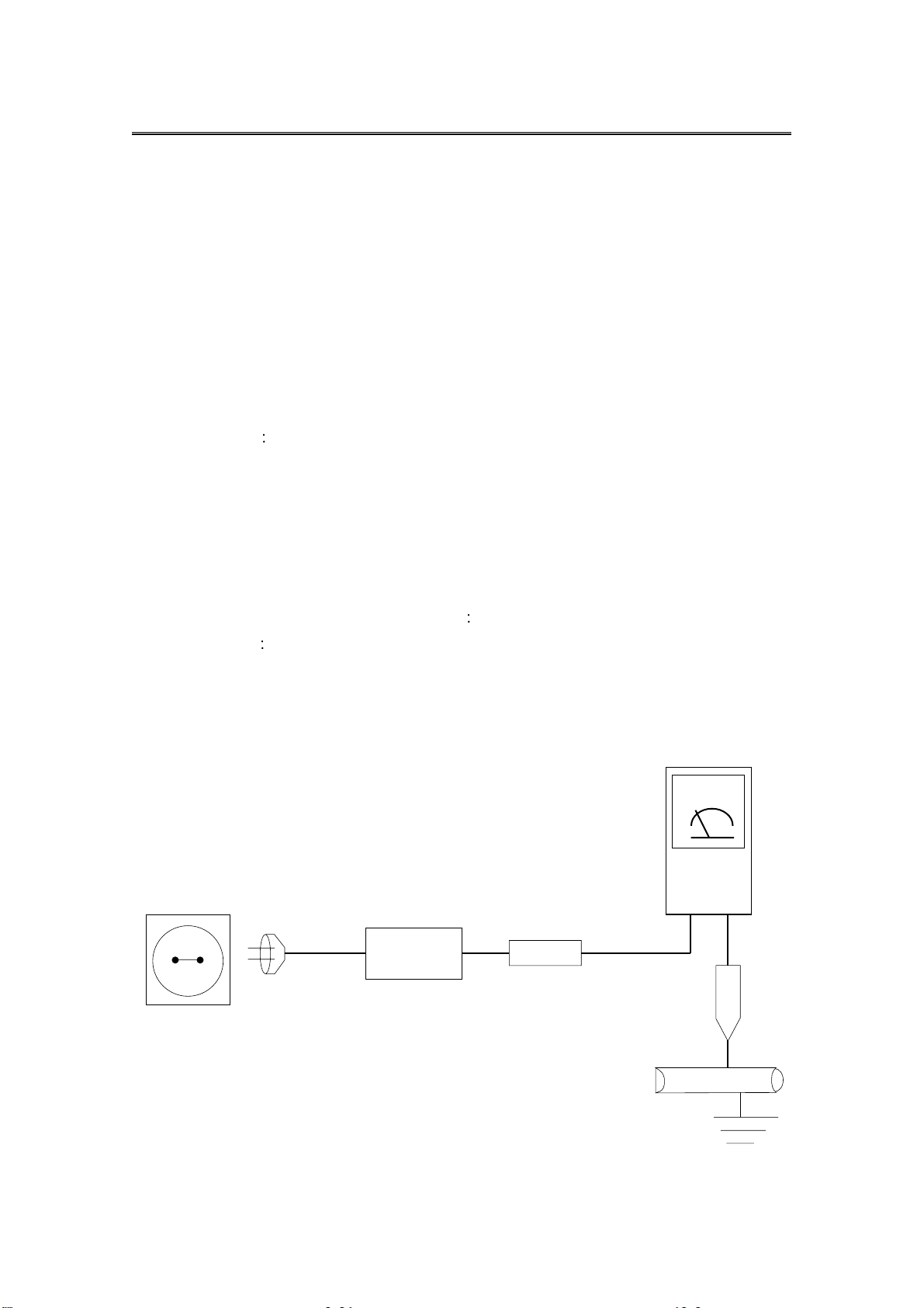
4. Leakage Current Hot Check (Figure 1-1)
Warning Do not use an isolation transformer during this test. Use a leakage current
tester or a metering system that complies with International Electrotechnical Commission
65.(IEC 65)
3
ALSO TEST WITH
PLUG REVERSED
POWER
CORD
TEST ALL
EXPOSED METAL
SURFACES
EARTH
GROUND
READING SHOULD NOT
BE ABOVE
<0.7mA PEAK AC<2mA DC.
FIGURE 1-1
AC LEAKAGE TEST
DEVICE
UNDER
TEST
LEAKAGE
CURRENT
TESTER
Page 4

5. With the unit completely reassembled, plug the AC line cord directly to the power outlet.
With the unit s AC switch first in the ON position and then OFF, measure the current
between a known earth ground (metal water pipe, conduit, etc.) and all exposed metal
parts, including
handle brackets, metal cabinets, screwheads and control shafts.
The current measured should not exceed < 0.7 mA peak AC < 2mA DC.
Reverse the power-plug in the AC outlet and repeat the test.
6. X-ray Limits
The picture tube is especially designed to prohibit X-ray emissions.
To ensure continued X-ray protection, replace the picture tube only with one that is the
same type as the original. Carefully reinstall the picture tube shields and mounting
hardware these also provide X-ray protection.
7. High Voltage Limits
High voltage must be measured each time servicing is done on the +B, horizontal
deflection or high voltage circuits.
8. High voltage is maintained within specified limits by close-tolerance, safety-related
components and adjustments. If the high voltage exceeds the specified limits, check
each of the special components.
9. Design Alteration Warning
Never alter or add to the mechanical or electrical design of this unit.
Example Do not add auxiliary audio or video connectors. Such alterations might
create a safety hazard. Also, any design changes or additions will void the
manufacturer s warranty.
10. Components, parts and wiring that appear to have overheated or that are otherwise
damaged should be replaced with parts that meet the original specifications. Always
determine the cause of damage or overheating, and correct any potential hazards.
11. Observe the original lead dress, especially near the following areas
Antenna wiring, sharp edges, and especially the AC and high voltage power supplies.
Always inspect for pinched, out-of-place, or frayed wiring.
Do not change the spacing between components and the printed circuit board. Check
the AC power cord for damage. Make sure that leads and components do not touch
thermally hot parts.
12. Picture Tube Implosion Warning
The picture tube in this receiver employs
"
integral implosion"protection.
To ensure continued implosion protection, make sure that the replacement picture tube
is the same as the original.
13. Do not remove, install or handle the picture tube without first putting on shatterproof
goggles equipped with side shields.
Never handle the picture tube by its neck. Some
"
in-line"picture tubes are equipped
with permanetly attached diflection yoke do not try to remove such "permanently
attached
"
yokes from the picture tube.
4
Page 5

14. Product Safety Notice
Some electrical and mechanical parts have special safety-related characteristics which
might not be obvious from visual inspection.
These safety features and the protection they give might be lost if the replacement
component differs from the original-even if the replacement is rated for higher voltage,
wattage, etc.
Components that are critical for safety are indicated in the circuit diagram by
shading( )
Use replacement components that have the same ratings, especially for flame
resistance and dielectric strength specifications. A replacement part that does not have
the same safety characteristics as the original might create shock, fire or other hazards.
1-2. Servicing Precautions
Warning 1 First read the "Safety Precaution"section of the manual.
If some unforeseen circumstance creates a conflict between the servicing and
safety precautions, always follow the safety precaution.
Warning 2
An electrolytic capacitor installed with the wrong polarity might explode.
1. Servicing Precautions are printed on the cabinet. Follow them.
2. Always unplug the unit
s AC power cord from the AC power source before attempting
to
(a) Remove or reinstall any component or assembly, (b) Disconnect an electrical
plug or connector, (c) Connect a test component in parallel with an electrolytic capacitor.
3. Some components are raised above the printed circuit board for safety.
An insulation tube or tape is sometimes used. The internal wiring is sometimes clamped
to prevent contact with thermally hot components.
Reinstall all such elements to their original position.
4. After servicing, always check that the screws, components and wiring have been
correctly reinstalled. Make sure that the portion around the serviced part has not been
damaged.
5. Check the insulation between the blades of the AC plug and accessible conductive parts
(examples metal panels,. input terminals).
6. Insulation Checking Procedure
Disconnect the power cord from the AC source and
turn the power switch ON. Connect an insulation resistance meter (500V) to the blades of
the AC plug.
The insulation resistance between each blade of the AC plug and accessible conductive
parts (see above) should be greater than 1 megohm.
7. Never defeat any of the B+ voltage interlocks. Do not apply AC power to the unit (or any
of its assemblies) unless all solid-state heat sinks are correctly installed.
5
Page 6

8. Always connect a test instrument s ground lead to the instrument chassis ground before
connecting the positive lead always remove the instrument s ground lead list.
1-3. Precautions for Electrostatically Sensitive Devices (ESDs)
1. Some semiconductor ("solid state") devices are easily damaged by static electricity.
Such some components are called Electrostatically Sensitive Devices (ESDs) examples
include integrated circuits and some field-effect transistors. The following techniques will
reduce the occurrence of component damage caused by static electricity.
2. Immediately before handling any semiconductor components or assemblies, drain the
electrostatic charge from your body by, touching a known earth ground. Alternatively,
wear the discharging wrist-strap device. (Be sure to remove it prior to applying powerthis is an electric shock precaution)
3. After removing an ESD-equipped assembly, place it on a conductive surface such as
aluminum foil to prevent accumulation of electrostatic charge.
4. Do not use freon-propelled chemicals. These can generate electrical charges that
damage ESD
S.
5. Use only a grounded-tip soldering iron when soldering or unsoldering ESDS.
6. Use only an anti-static solder removal device. Many solder removal devices are not rated
as "anti-static" these can accumulate sufficient electrical charge to damage ESDS.
7. Do not remove a replacement ESD front its protective package until you are ready to
install it. Most replacement ESDs are packaged with leads that are electrically shorted
together by conductive foam, aluminum foil or other conductive materials.
8. Immediately before removing the protective material from the leads of a replacement
ESD, touch the protective material to the chassis or circuit assembly into which the
device will be installed.
9. Minimize body motions when unpackaged replacement ESDs. Motion, such as brushing
clothes together, or lifting a foot from a carpeted floor can generate, enough static
electricity to damage an ESD.
6
Page 7

2. Specifications
MODEL : CT21AF
DESCRIPTION : 21 INCH CCTV WITH 2 CH CAMERA INPUT &
HORIZONTAL RESOLUTION 450 LINES
1) SPECIFICATIONS
COLOR SYSTEM : NTSC 3.58 / PAL-B
POWER INPUT : AC 100-240V(50/60 Hz)
POWER CONSUMPTION : 67W
VIDEO IMPEDANCE : 75Ohm BNC
SOUND OUTPUT : 1.0
0.2W 8 Ohm
SPEAKER SIZE : 70mm
40mm
VIDEO OUTPUT LEVEL : 1.0V
p-p 10% at 75 Ohm
VIDEO INPUT LEVEL : 1.0V
p-p 10% at 75 Ohm
AUDIO OUTPUT LEVEL : RCA JACK TYPE
300
50mVrms
AUDIO INPUT LEVEL : RCA JACK TYPE
300
50mVrms
SOUND DISTORTION : Less Than 10%
HUM : Less Than 10mVrms
BUZZ : Less than 200mV
p-p
2) FEATURES
BLUE BACK AT NO SIGNAL
PROTECTION CIRCUIT FOR X-RAY
S-VHS INPUT
VIDEO THROUGH-OUT
3) CONTROLS & SWITCHES
MAIN AC POWER S/W : PUSH LOCK FRONT
PICTURE CONTROL : ROTARY FRONT
(CONTRAST, BRIGHTNESS, TINT, COLOR, SHARPNESS)
VOLUME CONTROL : ROTARY FRONT
S-VHS/CAMERA SELECTION : TACT SWITCH FRONT
VIDEO IMPEDANCE : SLIDE SWITCH BACK
7
Page 8

4) LIGHTINGS
INDICATOR : POWER ON (GREEN)
: VIDEO 1 (GREEN)
: VIDEO 2 (GREEN)
: Y/C (GREEN)
5) JACK & TERMINALS
4 BNC : VIDEO INPUT/OUTPUT
4 AUDIO RCA : AUDIO INPUT/OUTPUT
S-VHS MINI DIN : S-VHS INPUT
AC INLET : AC INPUT
6) ACCESSORIES
WARRANTY CARD
OWNER’S MANUAL
POWER CORD
7) CABINET SIZE
476(W) 432(H) 468(D)
8) PACKING
BOX OUT : 566(W) 555(H) 562(D)
Q’TY SET PER 40 FOOT FCL : 336 SETS
Q’TY SET PER 20 FOOT FCL : 160 SETS
9) REMARKS
WEIGHT : 26Kg
8
Page 9
9
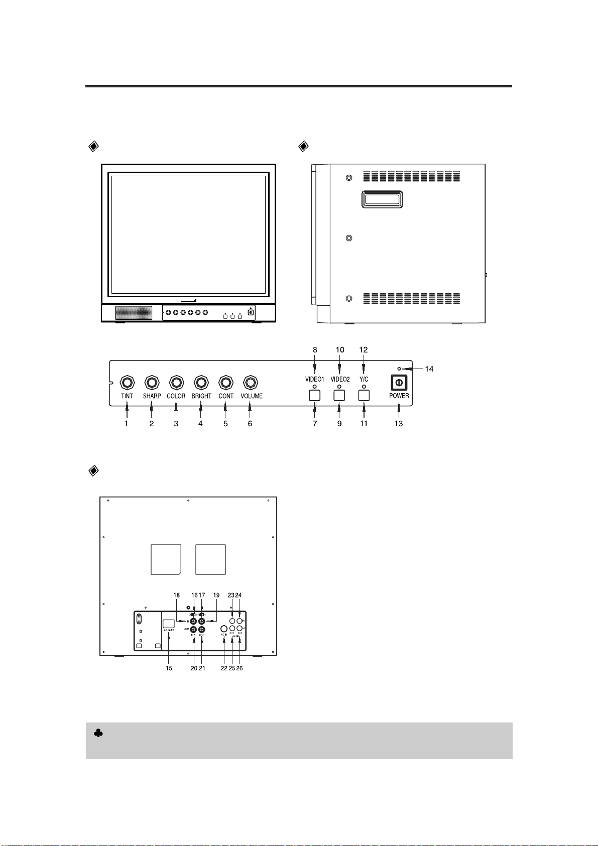
3. Description of controls
WARNING : TO PREVENT FIRE OR SHOCK HAZARD, DO NOT EXPOSE THIS
CCTV TO RAIN OR MOISTURE
Front View Side View
Rear View
1. TINT
2. SHARPNESS
3. COLOR
4. BRIGHTNESS
5. CONTRAST
6. VOLUME
7. VIDEO 1
8. VIDEO 1 LED LAMP
9. VIDEO 2
10. VIDEO 2 LED LAMP
11. Y/C
12. Y/C LED LAMP
13. POWER BUTTON
14. POWER LED LAMP
15. POWER INLET
16. IMPEDANCE (SLIDE S/W)
17. IMPEDANCE (SLIDE S/W)
18. CHANNEL 1 IN(BNC)
19. CHANNEL 2 IN(BNC)
20. CHANNEL 1 OUT(BNC)
21. CHANNEL 2 OUT(BNC)
22. Y/C IN(DIN)
23. CHANNEL 1 AUDIO IN(RCA)
24. CHANNEL 2 AUDIO IN(RCA)
25. CHANNEL 1 AUDIO OUT(RCA)
26. CHANNEL 2 AUDIO OUT(RCA)
Page 10
10
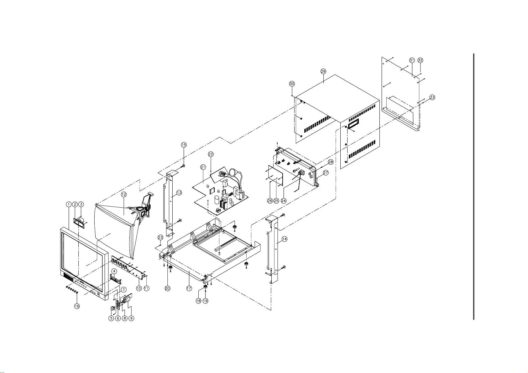
4. EXPLODED VIEW
Page 11
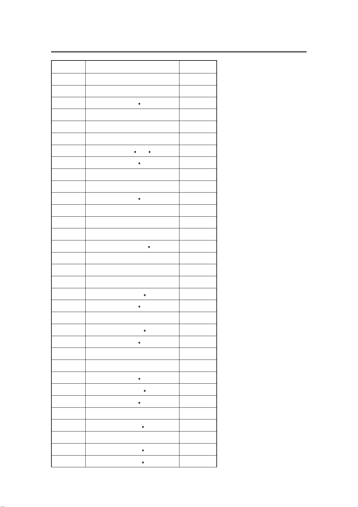
NO ITEM
Q’TY
1
2
3
4
5
6
7
8
9
10
11
12
13
14
15
16
17
18
19
20
21
22
23
24
25
26
27
28
29
30
31
32
33
FRONT PANEL ASS’Y
SPEAKER SYSTEM
SCREW BTB 3
10
KNOB, BLOCK
KNOB, POWER
BRACKET, POWER
SCREW PB 3 0.5 6
SCREW BTB 3 10
POWER S/W, MTR
CONTROL, MONITOR
SCREW BTB 3 10
CPT ASS’Y
BRACKET, LEFT
BRACKET, RIGHT
SCREW HTTBW 6 30
KNOB, VOLUME ASS’Y
BOTTOM COVER
RUBBER FOR LEG
SCREW BTBW 3
12
SCREW BTB 4
12
MAIN, CCTV
SCREW BTBW 3
12
SCREW BTB 4
12
BACK PANEL ASS’Y
BACK BOARD
SCREW BTB 3 10
SCREW BTBW 3 12
SCREW BTB 4 12
TOP COVER
SCREW BTTB 4 8
BRACKET, REAR
SCREW BTTS 3 8
SCREW PBTB 3
12
1
1
2
1
1
1
2
2
1
1
7
1
1
1
4
6
1
4
4
4
1
3
2
1
1
6
2
1
1
6
1
7
5
11
Page 12

5. Alignment and Adjustments
5-1. Preadjustment
5-1-1. Factory Mode
1. Do not attempt these adjustments in the VIDEO mode.
2. The Factory Mode adjustments are necessary when either the EEPROM(Q002) or the CPT
is replaced.
3. Do not tamper with the "Adjustment" screen of the Factory Mode menu. The screen is intended
only for factory use.
5-1-2. When EEPROM (Q002) is replaced
1. When Q002 is replaced all adjustment data revert to their initial values. It is necessary to reprogram this data.
2. After Q002 is replaced, warm up the CCTV SET for 10 seconds.
5-1-3. When CPT is replaced
1. Make the following adjustments after setting up purity and convergence:
White Balance
Vertical center
Vertical size
Horizontal size
5-2. Factory / Service Mode
5-2-1. Procedure for the "Adjustment" Mode
1. This mode uses the standard remote control. The Factory (Service) Mode is activated by
pressing the "Factory" key on the remote control.
2. The Factory Mode will be displayed. The Factory Mode has four components: Screen adjustment,
Position adjustment, White balance, and Volume Adjust.
3. Access the Adjustment Mode by pressing the VOLUME keys (Up or Down). The adjustment
Parameters adjusted are listed in the accompanying table, and they are selected by pressing
the PROGRAM keys (Up or Down).
4. The VOLUME keys increase or decrease the adjustment values, which are stored in the nonvolatile memory as soon as the adjustment is cancelled.
5. Cancel the Adjustment Mode by pressing the OUT CONDITION key.
12
Page 13
13
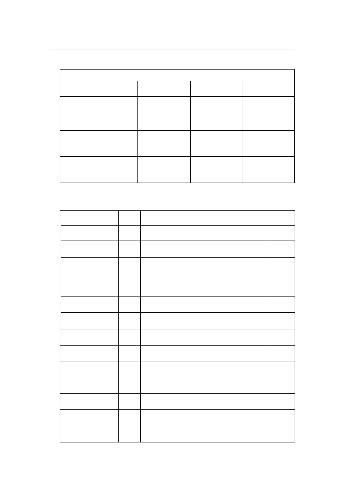
5-2-2. Service Adjustment Parameter
Main Adjustment Parameter
FUNCTION
OSD
ABBREVIATION
RANGE INITIAL DATA
SCREEN VOLTAGE
INCH OPTION
HORIZONTAL SHIFT
VERTICAL AMPLITUDE
VERTICAL SHIFT
VERTICAL SLOPE
RED CUTOFF
GREEN CUTOFF
BLUE CUTOFF
VOLUME OUTPUT
Screen ADJ
Inch
Hrs
Height
VRS
VS
R
G
B
Volume Adjust
---
21
0 ~ 63 Step
0 ~ 63 Step
0 ~ 63 Step
0 ~ 63 Step
0 ~ 63 Step
0 ~ 63 Step
0 ~ 63 Step
0 ~ 63 Step
---
21 inch
50
40
33
32
32
32
32
47
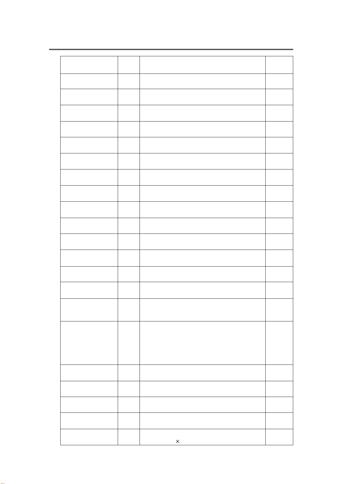
5-2-3. Factory Adjustment Parameter
FUNCTION OSD DESCRIPTION
INITIAL
DATA
IF Sensitivity
Modulation standard
Video mute switch
Search tuning mode
Video ident mode
AFC Window
PLL demodulator
frequency adjust
X-tal definition
Synchronisation
Phase 1 time constant
Video ident mode
Long blanking mode
Interlace
IFS
MOD
VSW
STM
VIM
AFW
LFA
XA
XB
POC
FOA
FOB
VID
LBM
DL
Off : Normal sensitivity
On : Maximum gain reduced by 20dB
Off : Negative modulation
On : Positive modulation
Off : Normal operation
On : IF video signal switched off
Off : Normal operation
On : Reduced dynamic sensitivity of
coincidence detector
Off : Ident coupled to CVBS
INT
On : Ident coupled to selected CVBS or Y/C
Off : Nominal window
On : Enlarged window
Off : Normal IF frequency
On : Frequency shift for L standard
0,0 : 3.6MHz, 3,6MHz, 0,1 : 3.6MHz, Open
1,0 : Open, 3,6MHz, 1,1 : 3.6MHz, 4.4MHz
Off : Active
On : Not active
0,0 : Normal, 0,1 : Slow
1,0 : Slow/Fast, 1,1 : Fast
Off : Phase 1 loop switched on and off
On : Not active
Off : Adapted to standard (50 or 60Hz)
On : Fixed in accordance with 50Hz standard
Off : Interlace
On : De-interlace
Off
Off
Off
Off
Off
Off
Off
1,1
Off
Normal
Off
Off
Off
Page 14
14
Forced field frequency
Vertical divider mode
Vertical overscan
Vertical scan disable
Helper output blanking
Enable vertical guard
Service blanking
Cathode drive level
Auto kine biasing
Automatic start up
RGB Blanking
Blue stretch
Black stretch
Enable fast blanking
Gain of luminance channel
Y-delay adjustment
Input source select
Fixed audio volume
Sound mute
Auto. volume leveling
Auto. Color limiting
Chroma bandpass
centre frequency
FORF
FORS
NCIN
OSO
VSD
HOB
EVG
SBL
CL 0
1 2
AKB
AST
RBL
BLS
BKS
IE1
GAI
YD
0123
IN
ABC
FAV
SM
AVL
ACL
CB
0,0 : Auto 60Hz, 0,1 : 60Hz forced
1,0 : Keep last detected freq., 1,1 : Auto 50Hz
Off : Normal
On : Switched to large search window
Off : Switch-off undefined
On : Switch-off in vertical overscan
Off : Vertical scan active
On : Vertical scan disabled
Off : Not active
On : Active
Off : Not active
On : Active
Off : Not active
On : Active
0 0 0 : 57V, 0 0 1 : 63V, 0 1 0 : 70V, 0 1 1 : 77V
1 0 0 : 84V, 1 0 1 : 91V, 1 1 0 : 99V, 1 1 1 : 107V
Off : Active
On : Not active
Off : Automatic mode
On : Switch on under control of u-processor
Off : Not active
On : Active
Off : Not active
On : Active
Off : Not active
On : Active
Off : Not active
On : Active
Off : Normal gain
On : High gain
0 0 0 0 : 0ns, 0 0 1 0 : 40ns, 0 1 0 0 : 80ns
0 1 1 1 : 12ns, 1 0 0 0 : 160ns, 1 0 1 1 : 200ns
1 1 0 0 : 240ns, 1 1 1 0 : 280ns, 1 1 1 1 : 320ns
0 0 0 : Int CVBS + audio
0 0 1 : Ext CVBS + audio
0 1 0 : Y/C + Ext audio
0 1 1 : CVBS3 + Ext audio
1 0 0 : Y/C + Int audio
1 1 0 : Y/C + Ext audio
Off : Normal Volume control
On : Audio level output fixed
Off : Not active
On : Active
Off : Not active
On : Active
Off : Not active
On : Active
Off : Fsc
On : On : 1.1
Fsc
1,0
Off
On
Off
Off
Off
Off
0 0 0
Off
Off
Off
Off
On
Off
Off
1 1 1 0
0 0 1
Off
On
On
On
Off
Page 15
15
Enable ext. comb filter
Bypass chroma delay line
Matrix selection
Color decoder mode
Vertical S correction
Stand by
Overvoltage protection
detection
CMB
BPS
MAT
CM
012
SC
STB
PRD
Off : Disabled
On : Enabled
Off : Active
On : Bypassed
Off : Adapted to standard
On : Forced to PAL matrix
0 0 0 : Automatic
0 0 1 : Forced X-tal pin 34 PAL/NTSC
0 1 0 : Forced X-tal pin 34 PAL
0 1 1 : Forced X-tal pin 34 NTSC
1 0 0 : Forced X-tal pin 35 PAL/NTSC
1 0 1 : Forced X-tal pin 35 PAL
1 1 0 : Forced X-tal pin 35 NTSC
1 1 1 : Forced SECAM
63 Steps
Off : Stand by
On : Normal
Off : Overvoltage detection
On : Overvoltage detection and stop horizontal
drive(protection)
Off
Off
Off
0 0 0
10
On
On
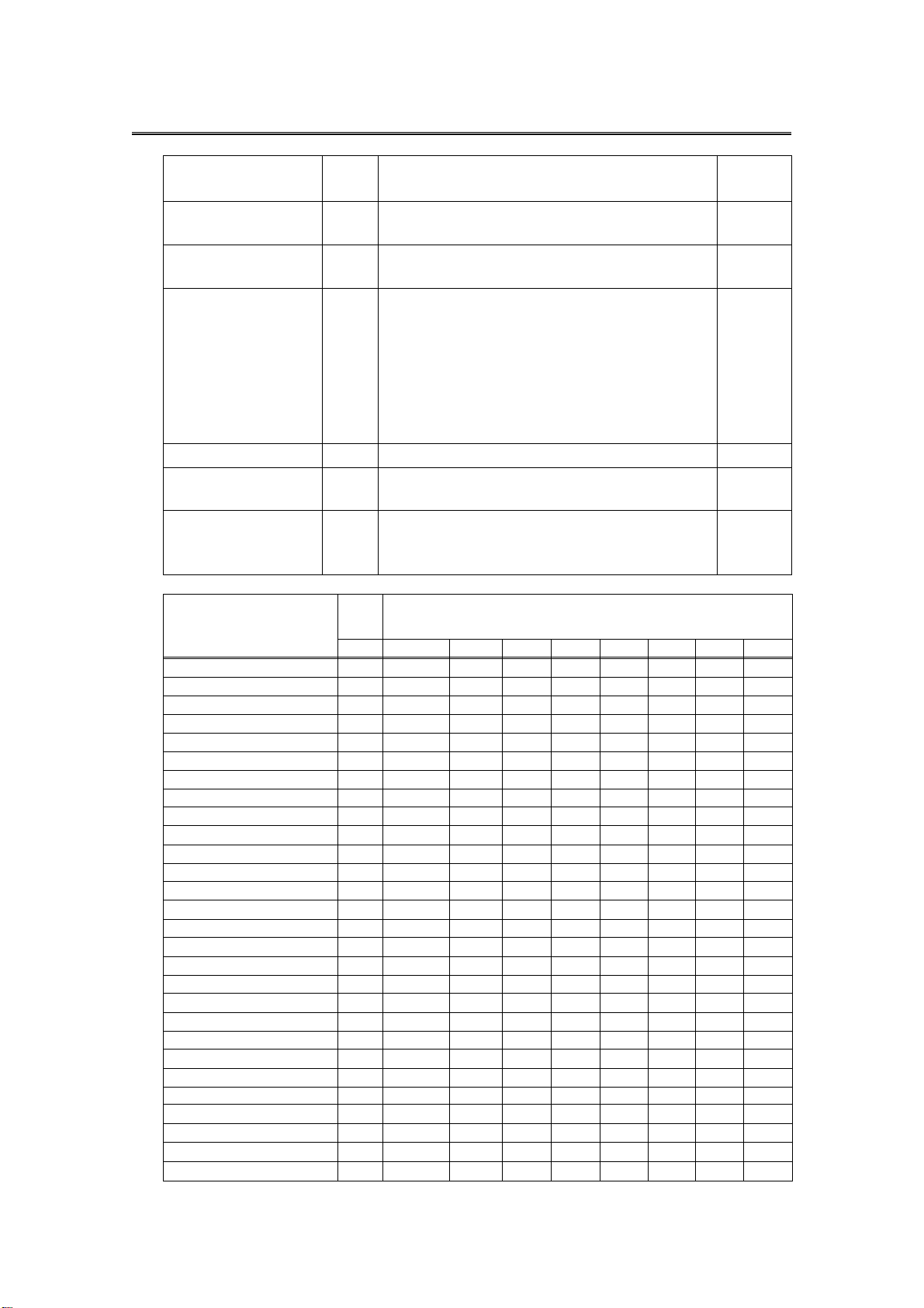
Input function
(Write)
Control 0
Control 1
Hue HUE
Horizontal shift HSH
E-W amplitude EW
E-W parabola/width PW
E-W corner parabola CP
E-W trapezium TC
Vertical slope VS
Vertical amplitude VA
S-Correction SC
Vertical shift VSH
White point Red WPR
White point Green WPG
White point Blue WPB
Peaking PEAK
Brightness BRI
Saturation SAT
Contrast CON
AGC Take over point TOP
Volume control VOL
IF Frequency selection IFFR
Vertical zoom VX
Vertical scroll VSC
Control 2
Control 3
Control 4
Control 5
00
01
02
03
04
05
06
07
08
09
0A
0B
0C
0D
0E
0F
10
11
12
13
14
15
16
17
18
19
1A
1B
INA
FORF
AVL/HBL
VIM
0
0
0
0
NCIN
VID
HCO
SBL
0
0
MAT
0
RBL
IE1
AFW
MOD
SM
IF A
0
0
OSO
HOB
YD3
0
INB
FORS
AKB
GAI
0
0
0
0
STM
LBM
EVG
PRD
0
0
0
0
COR
IE2
IFS
VSW
FAV
IFB
0
0
VSD
BPS
YD2
0
INC
DL
A5
A5
A5
A5
A5
A5
A5
A5
A5
A5
A5
A5
A5
A5
A5
A5
A5
A5
A5
IFC
A5
A5
CB
ACL
YD1
0
BCO
STB
A4
A4
A4
A4
A4
A4
A4
A4
A4
A4
A4
A4
A4
A4
A4
A4
A4
A4
A4
0
A4
A4
BLS
CMB
YD0
0
FOA
POC
A3
A3
A3
A3
A3
A3
A3
A3
A3
A3
A3
A3
A3
A3
A3
A3
A3
A3
A3
0
A3
A3
BKS
AST
DS
0
FOB
CM2
A2
A2
A2
A2
A2
A2
A2
A2
A2
A2
A2
A2
A2
A2
A2
A2
A2
A2
A2
0
A2
A2
CS1
CL2
DSA
0
XA
CM1
A1
A1
A1
A1
A1
A1
A1
A1
A1
A1
A1
A1
A1
A1
A1
A1
A1
A1
A1
0
A1
A1
CS0
CL1
FFI
0
XB
CM0
A0
A0
A0
A0
A0
A0
A0
A0
A0
A0
A0
A0
A0
A0
A0
A0
A0
A0
A0
0
A0
A0
BB
CL0
EBS
FCO
D7
D6
D5 D4 D3 D2 D1 D0
Sub
addr.
(hex)
Data bits
Page 16

16
5-2-4. Outcondition
The Outcondition Mode is used during factory inspection.
Function Reset
1. System Auto
5-3. Other Adjustments
5-3-1. General Alignment Instructions
1. Usually, a color CCTV needs only slight touch-up adjustment upon installation. Check the
basic characteristics such as height, horizontal and vertical sync and focus.
2. Observe the picture for good black and white details. There should be no objectionable
color, shading if color shading is present, perform the purity and convergence
adjustments described below.
3. Use the specified test equipment or its equivalent.
4. Correct impedance matching is essential.
5. Avoid overload. Excessive signal from a sweep generator might overload the front-end of
the CCTV SET. When inserting signal markers, do not allow the marker generator to distort
test results.
6. Connect the CCTV SET only to an AC power source with voltage and frequency as
specified on the backcover nameplate.
7. Do not attempt to connect or disconnect any wires while the CCTV SET is turned on.
Make sure that the power cord is disconnected before replacing any parts.
8. To protect against shock hazard, use an isolation transformer.
5-3-2. Automatic Degaussing
A degaussing coil is mounted around the picture tube, so that external degaussing after
moving the CCTV SET should be unnecessary.
But the receiver must be properly degaussed upon installation.
The degaussing coil operates for about 1 second after the power is switched ON. If the set is
moved or turned in a different direction, the power should be OFF for at least 10 minutes.
If the chassis or parts of the cabinet become magnetized, poor color purity will result. If this
happens, use an external degaussing coil. Slowly move the degaussing coil around the
faceplate of the picture tube and the sides and front of the receiver. Slowly withdraw the coil to
a distance of about 6 feet before turning power OFF.
If color shading persists, perform the following Color Purity and Convergence adjustments.
Page 17
17
5-3-3. High V oltage Check
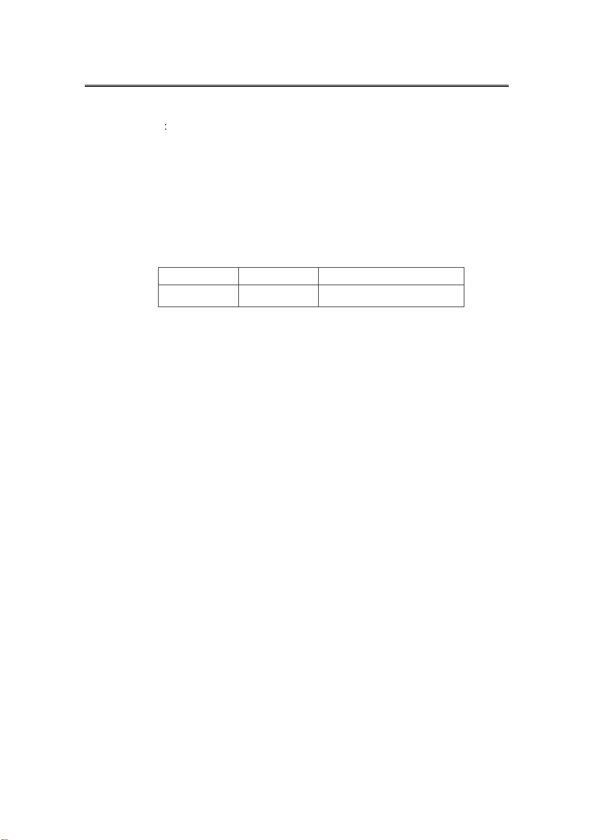
CAUTION There is no high voltage adjustment chassis. The B+power supply should be
+
135 volts (see table 1).
1. Connect a digital voltmeter to the second anode of the picture tube.
2. Turn on the CCTV SET. Set the Brightness and Contrast controls to minimum.
3. Adjust the Brightness and Contrast controls to both extremes.
Ensure that the high voltage does not exceed Maximum High voltage (see table 1) under
any conditions.
Table 1 +B and Maximum High voltage
5-3-4. FOCUS Adjustment
1. Input a cross dot signal.
2. Adjust the tuning control for clearest picture.
3. Adjust the FOCUS control for well defined scanning lines in the center area of the screen.
5-3-5. Screen Adjustment
1. Tune to the ACTIVE channel.
2. Adjust the FACTORY key is pressed on Remote Controller, Factory Mode shows up.
3. Selected OSD color is red.
4. When the VOL+key is pressed, the screen turns to one horizontal line.
5. Adjust SCREEN VR of FBT to make 1 dot bar.
6. After adjustment, once VOL+key is pressed again, it turns to FACTORY Mode.
5-3-6. Purity Adjustment
1. Warm up the receiver for at least 30 minutes.
2. Plug in the CRT deflection yoke. Tighten the clamp screw.
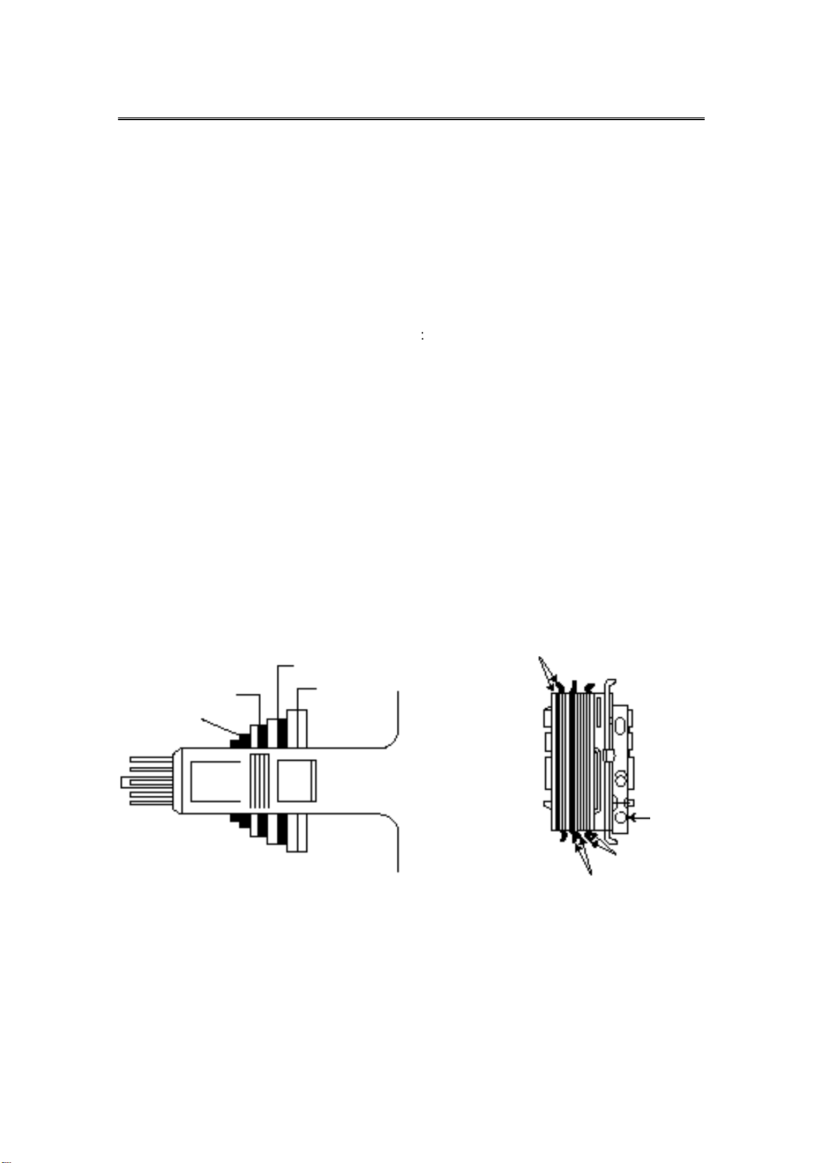
3. Plug the convergence yoke into the CRT and set it as shown in Fig. B-1.
4. Input a black and white signal.
5. Fully demagnetize the receiver by using an external degaussing coil.
6. Turn the CONTRAST and BRIGHTNESS controls to maximum.
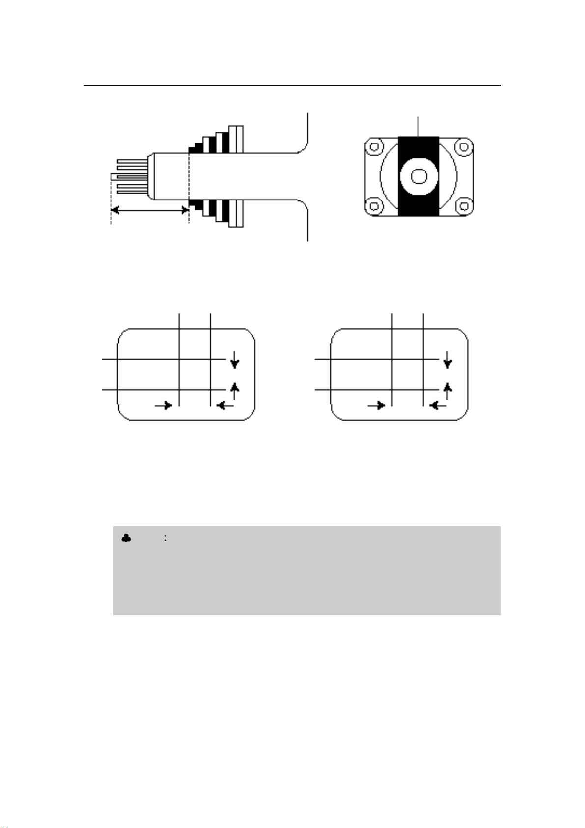
7. Loosen the clamp screw holding the yoke. Slide the yoke backward or forward to produce a
vertical green belt. (Fig. B-2)
8. Tighten the convergence yoke.
INCH
21
+
B (Volts)
135
Maximum High Voltage
27 KV
Page 18
9. Slowly move the deflection yoke forward. Adjust for the best overall green screen.
10. Temporarily tighten the deflection yoke.
11. Produce blue and red rasters by adjusting the-low-light controls.
Check for good purity in each field.
12. Tighten the deflection yoke.
5-3-7. Center Convergence Adjustment
1. Warm up the receiver for at least 30 minutes.
2. Adjust the two tabs of the 4-pole magnets Change the angle between them.
Superimpose the red and blue vertical lines in the center area of the screen.
3. Adjust the BRIGHTNESS and CONTRAST controls for a well-defined picture.
4. Adjust the two tabs of the 4-pole magnets, and change the angle between them.
Superimpose the red and the blue vertical lines in the center area of the screen.
5. Turn both tabs at the same time, keeping the angle constant, and superimpose the red and
blue horizontal lines in the center of the screen.
6. Adjust ing two-tabs of 6-pole magnets to superimpose the red and blue lines onto the green.
Adjusting the angle affects the vertical lines, and rotating both magnets affects the horizontal
lines.
7. Repeat adjustments 2-6, if necessary.
8. Since the 4-pole and 6-pole magnets interact, the dot movement is complex(fig B-3).
18
FIG. B-1 CONVERGENCE MAGNET ASSEMBLY
6 Pole Magnet
4 Pole Magnet
2 Pole Magnet
2 Pole
PURITY
4 Pole
CONVERGENCE
6 Pole
CONVERGENCE
YOKE
CLAMP
SCREW
Clamper
Screw
Page 19
19
5-3-8. White Balance Adjustment
1.
On Factory Mode, select number 3.
2. Press FACTORY key again to return to Factory Mode screen and select 1. White Balance.
3. In case of Screen adjustment, the color of horizontal bar can be used as a standard one and
use other two colors to adjust W/B.(AC 100 equipment used)
FIG. B-2 CENTER CONVERGENCE ADJUSTMENT
FIG. B-3 CENTER CONVERGENCE ADJUSTMENT
Vertical Green Belt
ADJUST
BLUE
BLUE
BLUERED RED
RED
BLUE/RED
GREEN
4-POLE MAGINETS MOVEMENT 6-POLE MAGINETS MOVEMENT
NOTE The purpose of this procedure is to optimize the picture tube to obtain
good black and white picture at all brightness levels while at the same
time achieving maximum usable brightness. Purity and convergence
adjustment must be processed in advance. Press the OUTCONDITION
key on the remote control unit.
Page 20
6. Using Devices and Description.
6-1. Main Signal Processor (TDA8842)
6-1-1. Feature
The following feature are available in all IC’S :
Multi-standard vision IF circuit with PLL demodulator
Alignment-free multi-standard FM sound demodulator (4.5MHz to 6.5MHz)
Flexible source selection with CVBS switch and Y(CVBS)/C input so that a comb filter can
be applied.
Integrated chrominance trap circuit
Integrated luminance delay line
Asmmetrical Peaking in the luminance channel with a noise coring function
Integrated chroma band pass filter with switchable center frequency
RGB control circuit with "Continuous Cathode Calibration" and white point adjustment
Possibility to insert a "Blue Back" option when no video signal is available
Horizontal synchronization with two control loops and alignment - free horizontal oscillator
Vertical count-down circuit
Vertical driver optimized for DC-coupled vertical output stages
I2C-bus control of various functions
20
Page 21
21
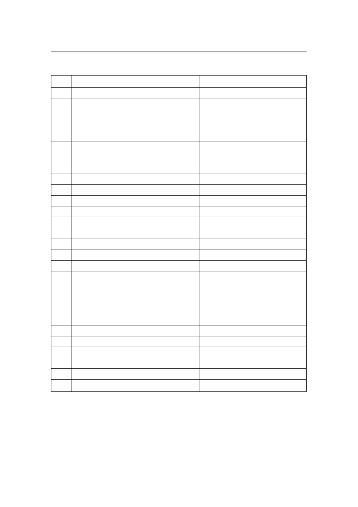
6-1-2. Pinning and Description
PIN DESCRIPTION
1
2
3
4
5
6
7
8
9
10
11
12
13
14
15
16
17
18
19
20
21
22
23
24
25
26
27
28
Sound IF input
External audio input
IF VCO tuned circuit 1
IF VCO tuned circuit 2
IF-PLL loop filter
IF video output
Serial clock input
Serial data input/output
Bandgap decoupling
Chrominance input
External CVBS
Main supply voltage 1 (+8V)
Internal CVBS input
Ground 1
Audio output
SECAM PLL decoupling
External CVBS input
Black-current input
Blue output
Green output
Red output
Beam current limiter input
Red input for insertion
Green input for insertion
Blue input for insertion
RGB insertion input
Luminance input
Luminance output
PIN DESCRIPTION
29
30
31
32
33
34
35
36
37
38
39
40
41
42
43
44
45
46
47
48
49
50
51
52
53
54
55
56
(B-Y) signal output
(R-Y) signal output
(B-Y) signal input
(R-Y) signal input
Subcarrier reference output
3.58MHz X-tal
4.43NHz X-tal
Loop filter phase detector
2ndsupply voltage 1 (+8V)
CVBS-1 output
Decoupling digital supply
Horizontal output
Flyback input/sandcastle output
Phase-2 filter
Phase-1 filter
Ground 2
East-west drive output
Vertical drive B output
Vertical drive A output
IF input 1
IF input 2
EHT/overvoltage protection input
Vertical sawtooth capacitor
Reference current input
AGC decoupling capacitor
Tuner AGC output
Audio deemphasis
Decoupling sound demodulator
Page 22
22
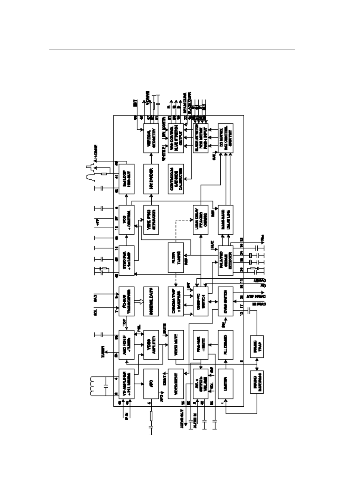
6-1-3. Block Diagram
I2C-bus controlled NTSC/PAL CCTV
Processors TDA884X/5X-N1 series
Page 23

6-1-4. Function Description
1. Audio
Alignment free multi standard PLL audio demodulator (4.5 to 6.5 MHz)
Volume control
2. Video
Integrated fixed luminance delay line
Integrated chroma trap (auto calibrated)
Integrated chroma bandpass filters with switchable center frequency (auto calibrated)
Asymmetrical peaking circuit in the luminance channel with switchable noise coring
function
Black stretching of non standard CVBS or luminance signals, switchable via IIC-bus
3. RGB
RGB control (brightness, contrast, saturation)
Improved black current stabilization (continuos cathode calibration)
White point adjustment
Blue stretch which offsets colors near white to blue
Option to insert "blue back" when no video signal is available
4. Input/Output
Flexible video source select with CVBS input for the internal signal and two external video
inputs (one switchable for CVBS or Y/C)
The output signal of the video source select is externally available (also as CVBS when Y/C
Y/C input is used)
External audio input
Linear RGB input with fast blanking
5. Synchronization and Deflection
Horizontal synchronization with two control loops and alignment free horizontal oscillator
Slow start and slow stop of the horizontal drive output to enable low stress start-up and
Switch-off from the line circuit at nominal line supply voltage.
Vertical count-down circuit for stable behavior with provisions for non-standard signals
Vertical geometry control
Vertical drive optimized for DC coupled vertical output stages
23
Page 24
24
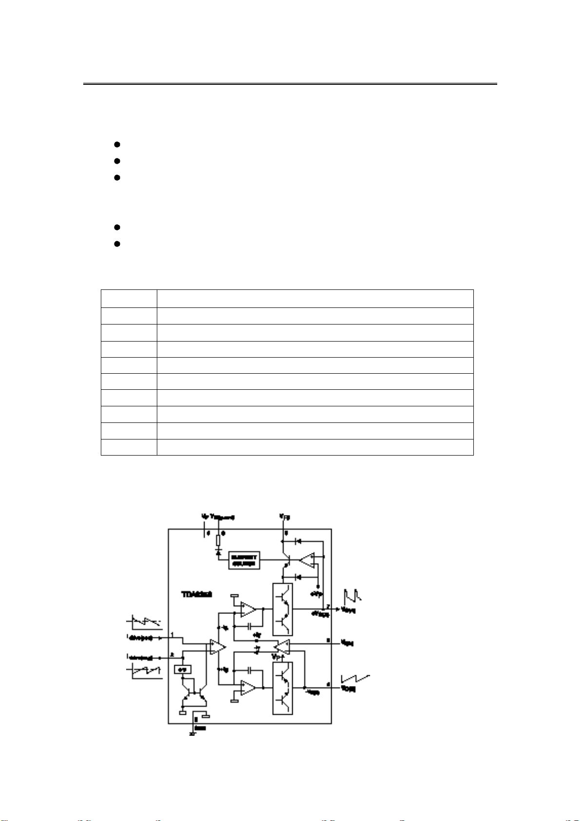
6-2. V ertical Output (TDA8351)
6-2-1. Feature
Highly efficient fully DC-coupled vertical output bridge circuit
Vertical flyback switch
Protection against:
Short-circuit of the output pins (7 and 4)
Short-circuit of the output pins to Vp
Temperature (thermal) protection
High EMC immunity because of common mode inputs
6-2-2. Pinning and Description
PIN DESCRIPTION
1
2
3
4
5
6
7
8
9
Input power stage (positive)
Input power stage (negative)
Operating supply voltage
Output voltage B
Ground
Input flyback supply voltage
Output voltage A
Guard output voltage
Input feedback voltage
6-2-3. Block Diagram
Page 25
25
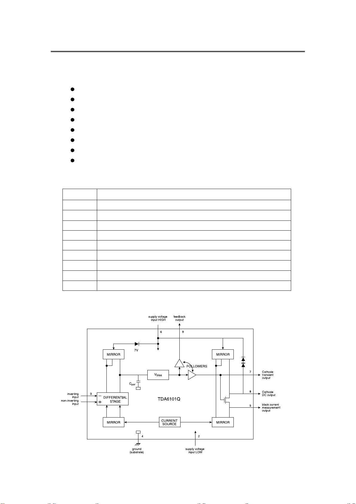
6-3. Video Output Amplifier (TDA6101Q)
6-3-1. Feature
Bandwidth : 9MHz typical at 100Vp-p
Slewrate : 1700 V/us
Only one supply voltage
Protection against ESD
Black-current measurement output for automatic black current stabilization
Internal reference voltage
Thermal protection
Defined switch-off behaviour
6-3-2. Pinning and Description
PIN DESCRIPTION
1
2
3
4
5
6
7
8
9
Non-inverting voltage input
Supply voltage low
Inverting voltage input
Ground
Black current measurement output
Supply voltage high
Cathode transient voltage output
Cathode DC voltage output
Feedback voltage output
6-3-3. Block Diagram
Page 26
26
6-4. Audio Output Amplifier (KA2201)
6-4-1. Feature
Wide operating supply voltage : Vcc=3V~14V.
Medium output power.
Low quiescent circuit current.
Good ripple rejection
Minimum number of external parts required.
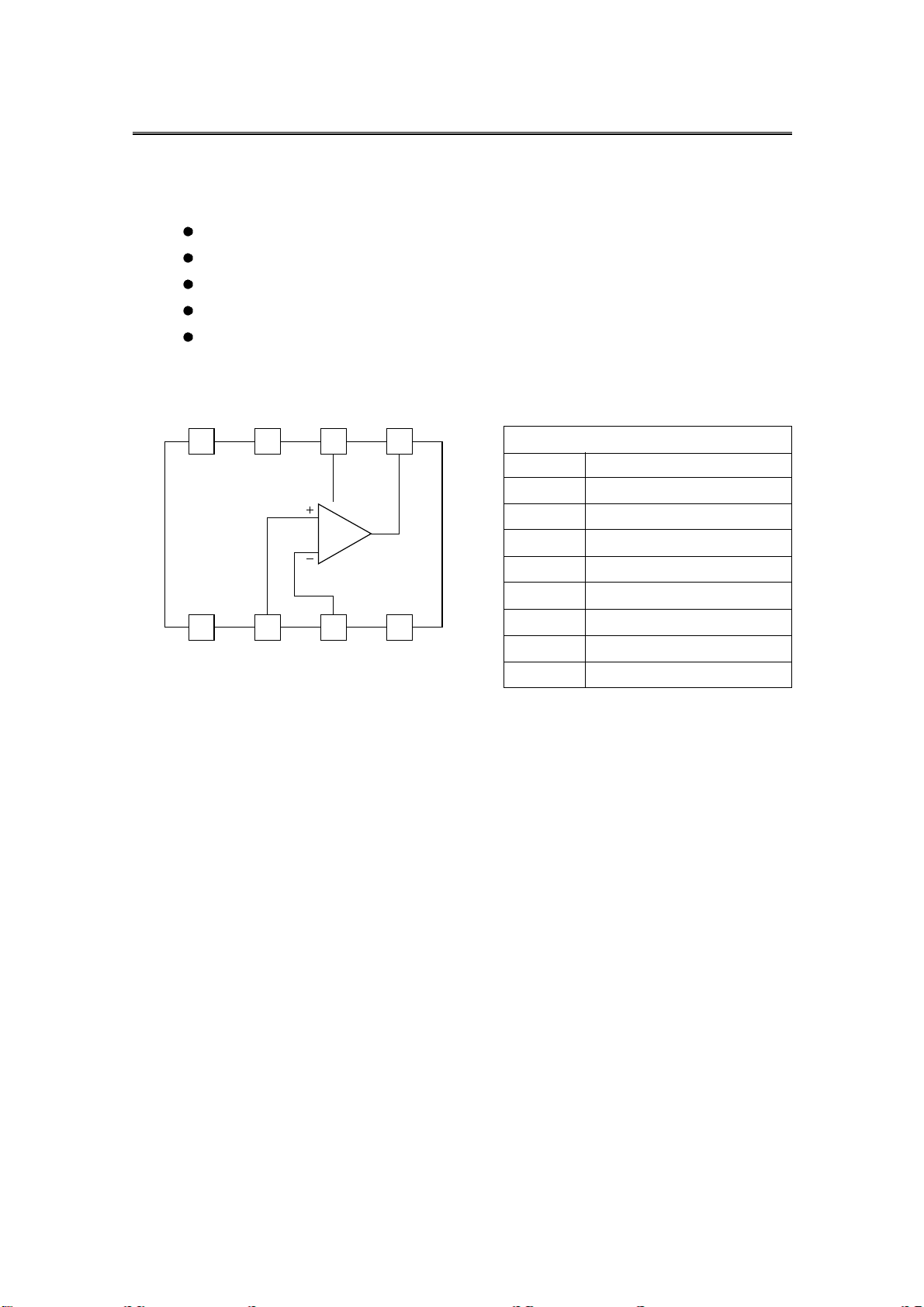
6-4-2. Pinning and Description
8 7
1 4
6 5
2 3
Pin Description
Pin Description
1
2
3
4
5
6
7
8
CB
NF
INPUT
GND
OUTPUT
Vcc
BOOTSTRAP
RIPPLE
Page 27
27
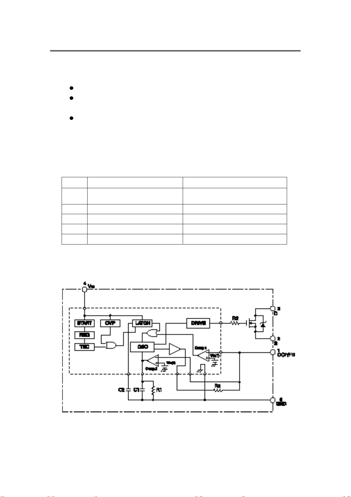
6-5. Power (STR-F6656)
6-5-1. Feature
Small SIP full mold package
Guaranteed avalanche energy :
Makes it possible to simplify surge absorbing circuit
Many protection functions :
Pulse-by-pulse overcurrent protection
Overvoltage protection with latch mode
Thermal protection with latch mode
6-5-2. Pinning and Description
PIN DESCRIPTION
1
2
3
4
5
Over current/Feedback terminal
Source terminal
Drain terminal
Power supply terminal
Ground terminal
DESCRIPTION
Input of overcurrent detection signal
and constant voltage control signal
MOS FET source
MOS FET drain
Input of power supply for control circuit
Ground
6-5-3. Block Diagram
Page 28
28
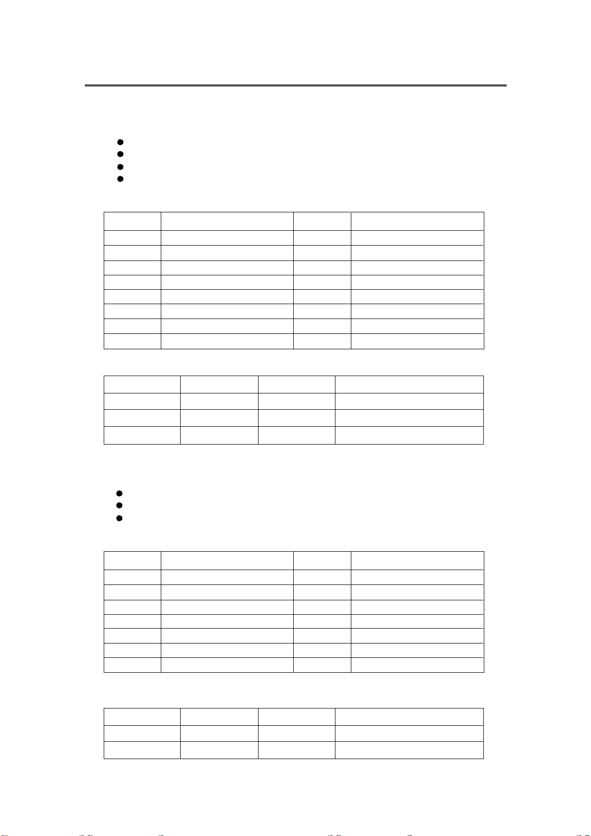
6-6. Video Select switch (CD4053BE)
6-6-1. Feature
SIP-16 Pin
Triple 2-Channel
Wide range of digital and analog signal levels digital 3 to 20V, analog to 20Vp-p
Low ON resistance : 125Ω(typ.)
6-6-2. Pinning and Description
PIN DESCRIPTION
1
2
3
4
5
6
7
8
Y1 Input
Y0 Input
Z1 Input
Z Output
Z0 Input
INH
VEE
Ground
PIN DESCRIPTION
9
10
11
12
13
14
15
16
Z Switch
Y Switch
X Switch
X0 Input
X1 Input
X Output
Y Output
Vcc
X Switch
L
H
H
Y Switch
H
L
H
OUTPUT
INPUT X
INPUT Y
INPUT Z
6-6-3. Control
Z Switch
H
H
L
6-7. Audio Select switch (CD4066BP)
6-7-1. Feature
SIP-14 Pin
Quiad Bilateral Switches
Low ON resistance : 120Ω(typ.)
6-6-2. Pinning and Description
PIN DESCRIPTION
1
2
3
4
5
6
7
Y0 IN/OUT Terminal
Z0 IN/OUT Terminal
Z1 IN/OUT Terminal
Y1 IN/OUT Terminal
E1 Enable Input
E2 Enable Input
VSS GROUND
PIN DESCRIPTION
8
9
10
11
12
13
14
Y2 IN/OUT Terminal
Z2 IN/OUT Terminal
Z3 IN/OUT Terminal
Y3 IN/OUT Terminal
E3 Enable Input
E0 Enable Input
VDD
AUDIO 1
AUDIO2
IN PUT
Y1
Y0
CONTROL SWITCH
E1 HIGH
E0 HIGH
6-7-3. Control
OUT PUT
Z1
Z0
Page 29
29
7. Technical Study (SMPS Operation)
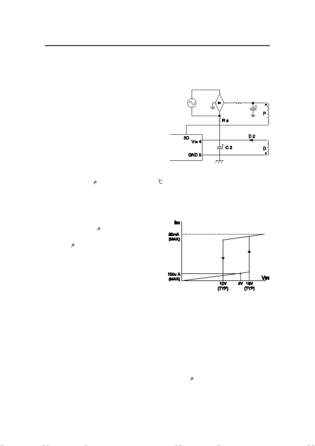
7-1. VIN terminal(pin 4) : Start-up circuit
The start-up circuit starts and stops the operation
of the control IC by detecting the voltage appearing
at the VIN terminal (pin 4).
The power supply (VIN terminal input) of the control
IC uses a circuit as shown in Fig. 1.
At start-up of the power supply, C2 is charged
through the start-up resistor Rs.
When the VIN terminal voltage reaches 16V
(typical), the control circuit starts operation by the
function of the start-up circuit.
As shown is Fig.2, since the circuit current is
suppressed to 100 Amax.(at VIN=141V, Tc=25 )
until the control circuit starts its operation, Rs can
be of high resistance.
Taking into account the slight increase of the
holding current (400
Amax.) of the latch circuit,
the Rs value shall be determined in a manner
that 500
A or higher current can flow even at the
lowest AC input voltage.
However, if the Rs value is too large, the current
charging C2 after switching on the AC input is
decreased to require longer time for reaching the
operation start voltage.
Therefore, the Rs value shall be examined
together with the C2 value which will be discussed
later.
The V
IN terminal voltage decreases after the control
circuit starts operation.
Therefore, if the C2 value is larger, the voltage drop ratio if the VIN terminal voltage is reduced.
Consequently, even if the drive winding voltage is delayed in rising, the VIN terminal voltage does
not drop to the shutdown voltage to maintain start-up function.
If the capacitance of C2 is too large, time from switch-on of AC input to operation start by C2
charging becomes longer.
In the typical power supply specifications, C2 may be 47 ~ 100
F for start-up.
Fig. 1 start-up circuit
Fig. 2 VIN terminal voltage circuit
current IIN
Page 30
30
After the control circuit starts its operation, power is
supplied by smoothing and rectifying the voltage of the
drive winding D which is provided in the transformer.
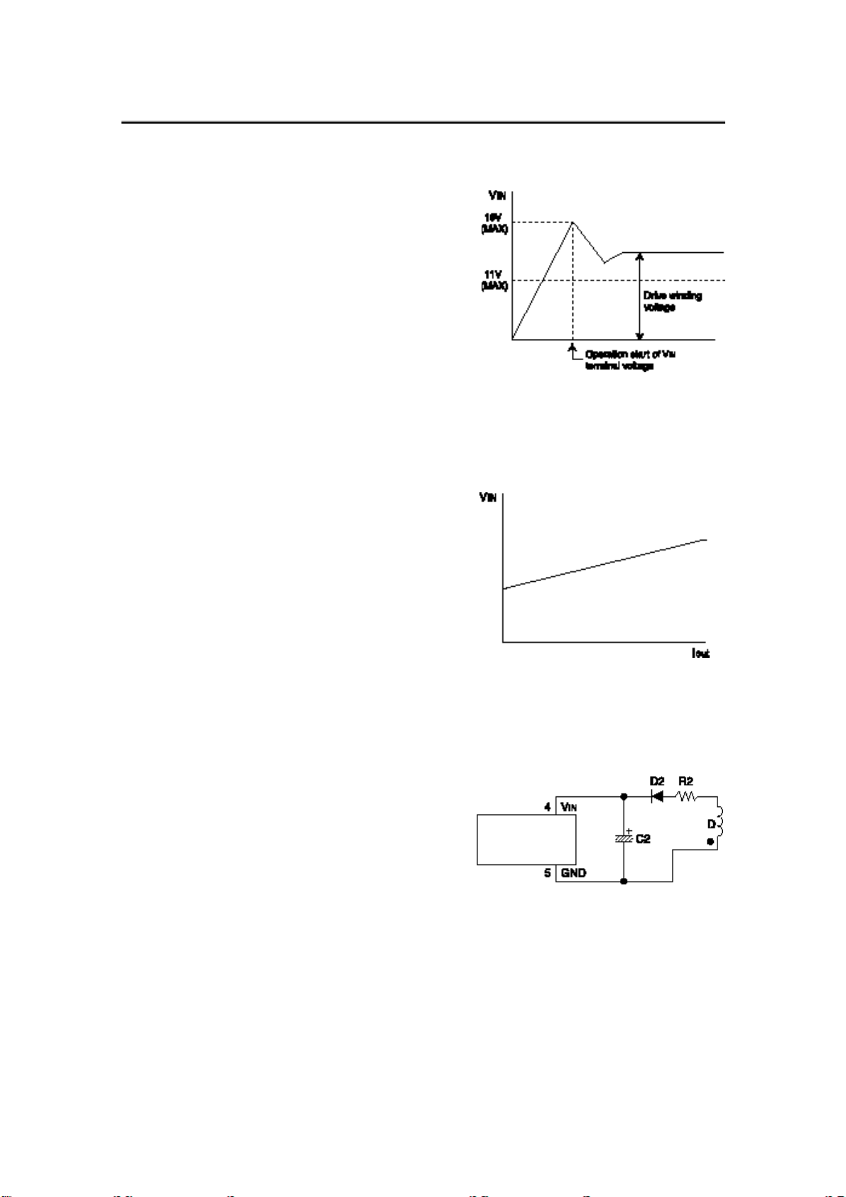
An example of the waveform of the V
IN terminal
voltage is shown in Fig. 3.
The drive winding voltage does not increase to the
set voltage immediately after the control circuit starts
its operation.
Although the V
IN terminal voltage starts decreasing,
the drive winding voltage reaches the set value
before the VIN terminal voltage drops to the shutdown
voltage which is set at such a low voltage as 10V.
Consequently, the control circuit can continue its
operation.
The turn number of the drive winding must be
determined in a manner that the C2 voltage can
be above the shutdown voltage [V
IN(OFF) 11V(MAX) ]
and below the OVP operating voltage [VIN(OVP)
20.5V(MIN) ].
However, in the actual power supply circuit, the
VIN
terminal voltage may vary subject to the secon-
dary side output current, as shown in Fig. 4.
This is because peak charging of C2 is performed
by surge voltage generated instantaneously at
MOS FET due to small circuit current of the IC.
In this case, by adding a resistor with several ohm
to several tens ohm in series with the rectifier diode,
this problem can be eased.
As to the optimal resistance value of the additional
resistor, as the variation ratio of the V
IN terminal
voltage is not same due to the construction of the
transformer used, it must be determined in accordance with the transformer actually used.
The variation ratio of the V
IN terminal voltage to the
output voltage becomes worse in proportion to the
worsening of the primary-secondary coupling of the
transformer and the coupling between the drive
winding and output stabilizing winding(winding for
a circuit regulating the constant voltage).
In designing the transformer, the above should be
taken into account.
Fig. 3 Waveform of VIN terminal
voltage at start-up
Fig. 4 Output current Iout - V
IN
terminal voltage
Fig. 5 Stabilized back-up power supply
circuit against output current Iout
Page 31

31
7-2. OCP/F.B. terminal (pin 1) :
Oscillator and constant voltage control circuit.
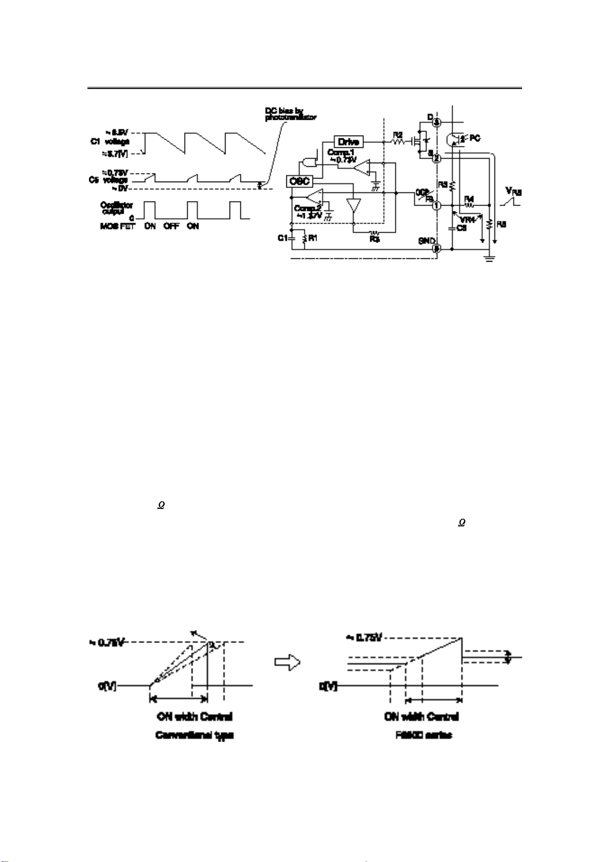
The Oscillator makes use of charging and discharging of C1 incorporated in the hybrid IC and
generates pulse signals to determine the OFF-time of the MOS FET.
The constant voltage control of a switch mode power supply is performed by fixing the OFF-time
of the MOS FET (=50
sec.) and changing the ON-time in the PRC(Pulse Ratio Control) operation.
Fig. 6 show how the oscillator works when the hybrid IC operates without control of constant voltage.
When the MOS FET is on, the capacitor C1 is charged to the constant voltage (=6.5V).
On the other hand, voltage drop (VR5) is caused in the OCP/FB terminal(pin 1) by the flow of drain
current across R5. This voltage is the a sawtooth voltage like ID and almost the same voltage as
applied to VR5 is applied to No. 1 terminal.
When the No. 1 terminal voltage reaches the threshold voltage Vth(1)=0.73V, the Comp.1 operates
and the comparator of the internal oscillator is reversed to turn off the MOS FET.
When the MOS FET turn off, charging of C1 is released and C1 starts discharging by the internal
resistor R1.
C1 voltages decrease in accordance with the slope which is determined by the discharging time
constants of C1 and R1.
When C1 voltages decrease to around 3.7V, the oscillator output is reversed again and the MOS
FET turns on.
Then, C1 is quickly charged to around 6.5V.
The MOS FET continues oscillation by repeating this operation.
As described above, the time determined by the slope of VR5(ID) is the ON-time of the MOS FET.
Also, the fixed time determined by C1 and R1 is the OFF-time of the MOS FET. The fixed time is
adjusted at around 50
sec. by function trimming of R1.
Fig. 6 Oscillating operation of switch-mode power supply
Page 32
32
For the control of the output, the feedback current (FB current) flowing to a photocoupler flows across
R4 and voltage drop VR4 thus caused is added to VR5.
The VR5 voltage (peak value of ID) which is necessary for the inversion of the Comp.1 is controlled
by VR4 (FB current) to change the height of ID peak value and VR4 controls the secondary side output
(current mode control).
R4 has a function of stabilizing the operation at light load.
Normally bias by VR4 increases at light load.
Without R4, R5 increases abnormally due to noise caused by surge current at MOS FET off, resulting
in wrong operation of Comp.1.
In order to prevent this trouble, the OCP/FB terminal (pin 1) is connected by R4 to the ground at low
impedance(560 ), while the MOS FET is off.
Then, the impedance of the OCP/FB terminal is reduced around by 1/2 (when R4=680 ) and the
bias of R4 is reduced by around 1/2 at the moment of turning on.
Thus, C5 absorbs noise caused at turn-on of the MOS FET.
In the conventional M6540 series, the photocoupler varies the slope of charging time until reaching the
threshold voltage Vth(1)=0.73V, but in F6500 series, DC bias control is used.
Fig. 7 Oscillating operation at constant voltage control
Page 33
33
7-3. OCP/F.B terminal (pin 1) OCP circuit
This is a pulse-by-pulse overcurrent protection circuit
which detects the peak of the peak of the drain current of
the MOS FET in every pulse and reverses the oscillator
output.
Fig. 7 shows the overcurrent detection circuit.
The MOS FET drain current is detected by inputting the
voltage drop of R5 connected between the source
terminal(pin 2) of the MOS FET and the GND terminal
(pin 5) into the OCP/FB terminal.
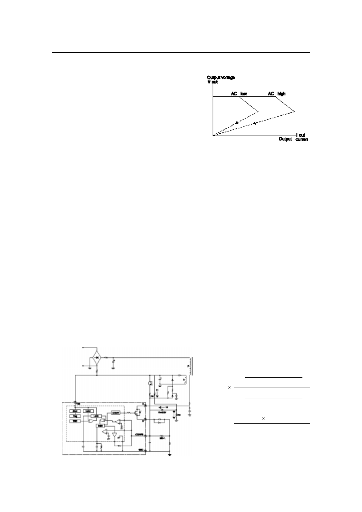
Fig. 8 shows the output characteristics of the secondary side at the time when the overcurrent
protection circuit operates due to the overload of the secondary side.
When the output voltage drops in the overload condition, the drive winding voltage of the primary
side also goes down proportionally, and the V
IN terminal voltage drops below the shutdown voltage
to stop the operation. In this case, as the circuit current also decreases simultaneously, the V
IN
terminal voltage increases again and the circuit operates intermittently by restoring the operation
start voltage. However, if there are a lot of output windings, even if overloaded output voltage drops,
the primary winding voltage may not drop so much and the operation may not be intermittent.
In STR-F6500 series, as the drain current of the MOS FET is detected for overcurrent protection,
the output power becomes high as the input voltage becomes high as shown in Fig. 8.
In order to prevent this high power, it is effective to add as shown if Fig. 9 a circuit by applying bias
which is in proportion with input voltage.
There are two advantages in providing this additional circuit.
(1) The drain current of the MOS FET can be suppressed to low level, when the input voltage
is high, therefore voltage stress to the MOS FET at start-up or overload can be reduced by
reducing surge voltage produced by the transformer.
(2) Current stress to the secondary side rectifier diode can be reduced by limiting the output
power in a certain degree.
Fig. 8 Power supply output
overload characteristic
Fig. 9 Compensation circuit of overcurrent protection by input voltage
RA = 680
1Dpeak(MAX) - 1Dpeak(MIN)
VIN(DC)MAX - VIN (DC)MIN
1Dpeak(MAX)
0.73
RB =
VIN(DC)MIN - (6.8 + 0.73)
RA
(6.8 + 0.73)
Page 34
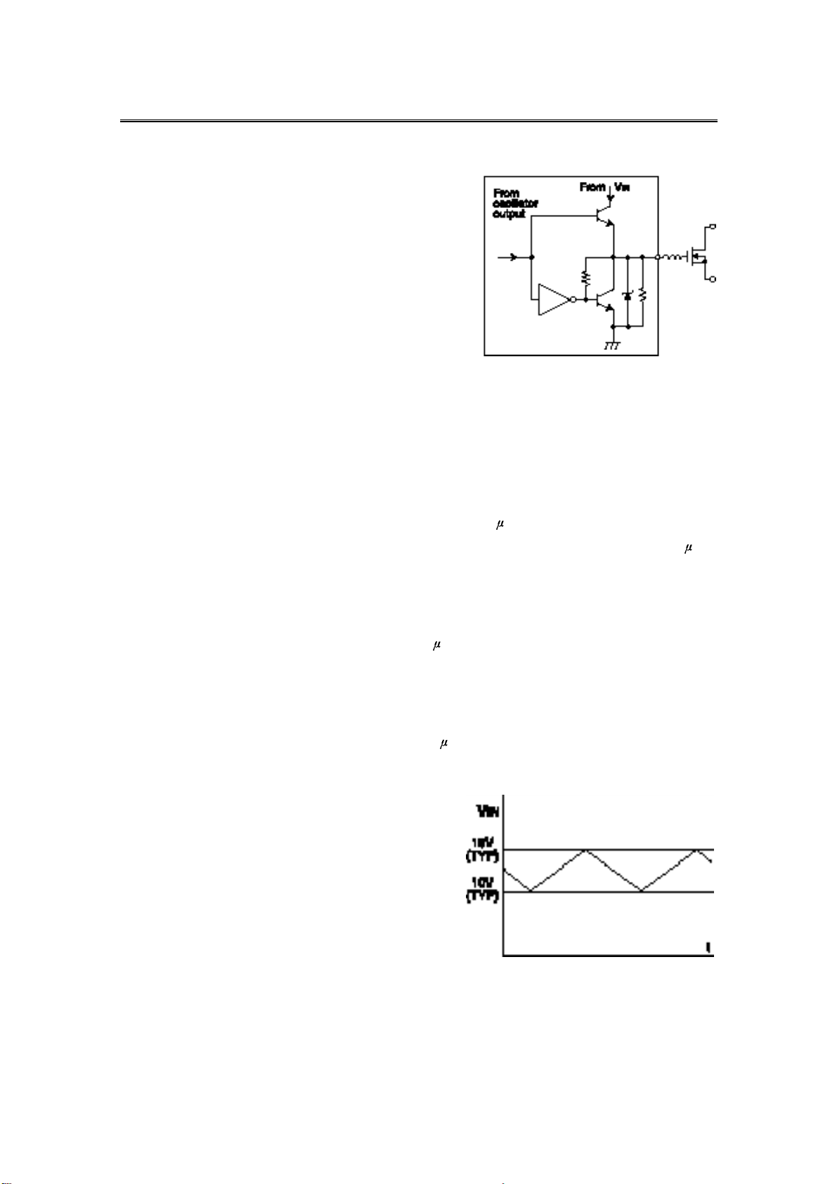
7-4. Drive circuit
This circuit charges and discharges the capacitance
between the gate and the source of the power MOS
FET by receiving pulses from the oscillator. As shown
in Fig.10, the basic circuit configuration is totem-pole
type connection of transistors and the maximum source
current is 0.2A and the maximum sink current is 0.3A.
As this current can sink even when the V
IN voltage is
lower than the shutdown voltage, the drive circuit turns
off the MOS FET without fail.
7-5. Latch circuit
The latch circuit is a circuit which keeps an output from the oscillator low and stops operation of
the power supply when overvoltage protection(OVP) and thermal shutdown(TSD) circuits are in
operation. As the sustaining current of the latch circuit is 400
A maximum when the VIN terminal
voltage is 8.5V, the power supply circuit sustains the OFF-state as long as the current of 400 A
minimum flows to the VIN terminal from the start-up resistor.
In order to prevent a malfunction caused by noise, etc., delay time is provided by C2 incorporated
in the hybrid IC and therefore, the latch circuit operates when the OVP or TSD circuit is in operation or and external signal input is provided for 10
sec. or longer.
In addition, even after the latch circuit start operating, the constant voltage regulator(Reg) circuit is
in operation and the circuit current is at a high level. As a result, the V
IN terminal voltage rapidly
decreases. When the VIN terminal voltage become lower than the shutdown voltage (10V typ), it
starts increasing as the circuit current is below 400 A. When it reaches the operation start voltage
(16V typ), the VIN terminal voltage decreases as the circuit current increases again.
When the latch circuit is on, the V
IN terminal
voltage increases and decreases within the range
from 10V(typ) to 16V(typ) and is prevented from
abnormally increasing. Fig. 11 shows and
example of the VIN terminal voltage waveform
when the latch circuit is in operation.
Cancellation of the latch circuit is done by
decreasing the V
IN terminal voltage blow 6.5V.
Usually the power supply can be restarted by
shutting down and an AC input to the power
supply once.
34
Fig. 10 Drive circuit
Fig. 11 Example of V
IN terminal voltage
waveform at latch circuit on
Page 35

35
7-6. Thermal shutdown circuit
This circuit triggers the latch circuit when the frame temperature of the hybrid IC exceeds 140
(typ).
The temperature is actually sensed by the control IC, but it also works against overheating of the
MOS FET as the MOS FET and the control IC are mounted on the same lead frame.
7-7. Overvoltage protection circuit
This circuit triggers the latch circuit when the VIN voltage exceeds 22.0V(typ).
Although it basically functions as protection of the V
IN terminal against overvoltage, since the VIN
terminal is supplied from the drive winding of the transformer and the voltage is proportional to the
output voltage, it also prevents overvoltage at the secondary output which is caused when the
control circuit is open circuited or by some other event. In this case, the secondary output voltage
at the time when the overvoltage protection is on can be obtained from the following equation.
Vout(OVP)
22.5V(typ)
Output voltage V out in normal operation
V
IN terminal voltage in normal operation
Page 36
36
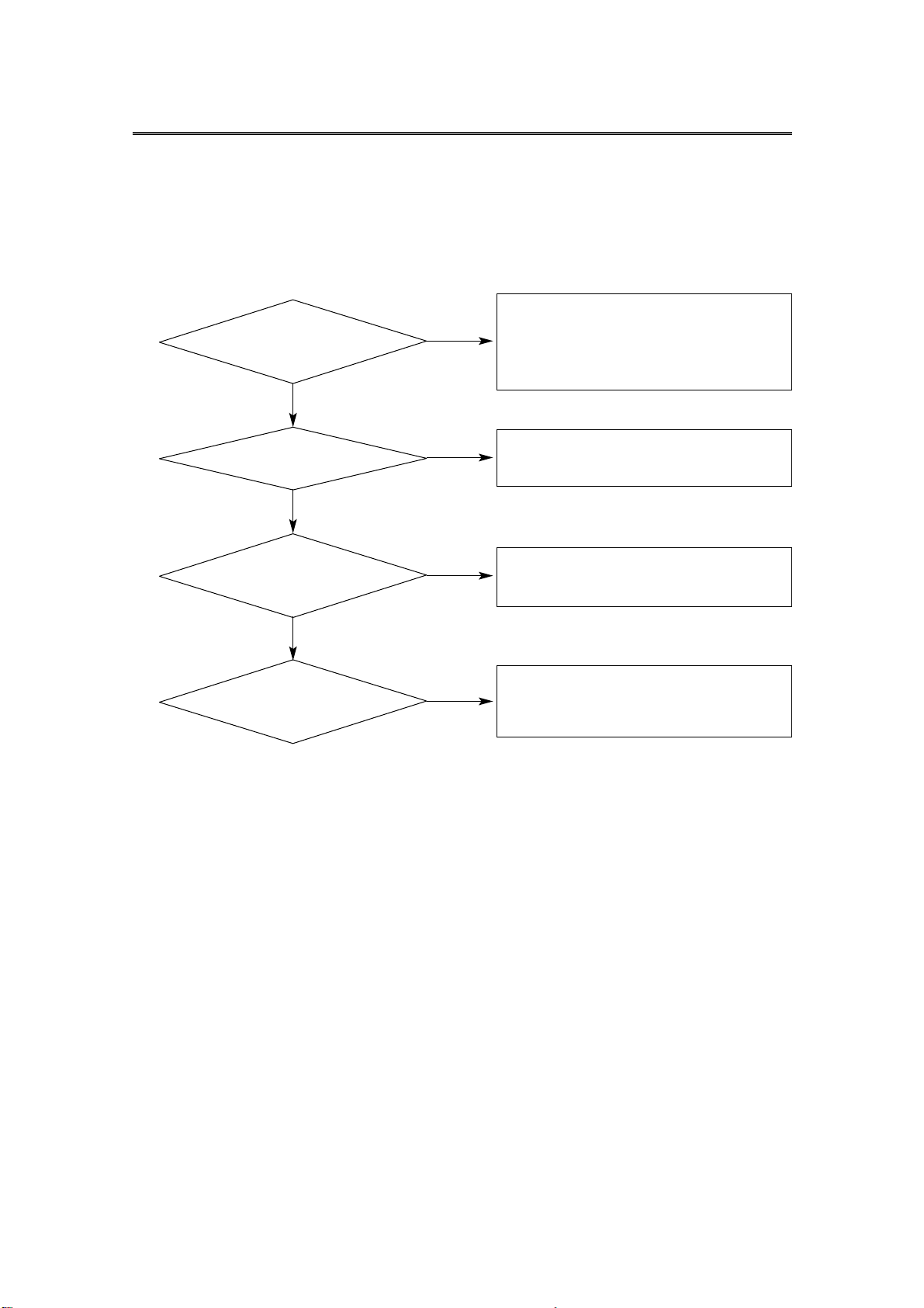
8. Trouble Shooting
8-1. No Power
Check the voltage
between + and - of C805
Check the pin 1, 3
of Q807
Check the voltage
between + and - of C822
Check the pin 3 of Q805
1) Check F801
IF F801 is broken, replace it after checking this :
D801, D802, D803, D804
2) Check Q801
Check Q501, Q901, Q902, Q903
Check Q404, Q401
NO
Check Q805, D825, T801
Check Q001 Pin 34
NO
Check Q807, D825
NO
NO
YES
YES
YES
Page 37
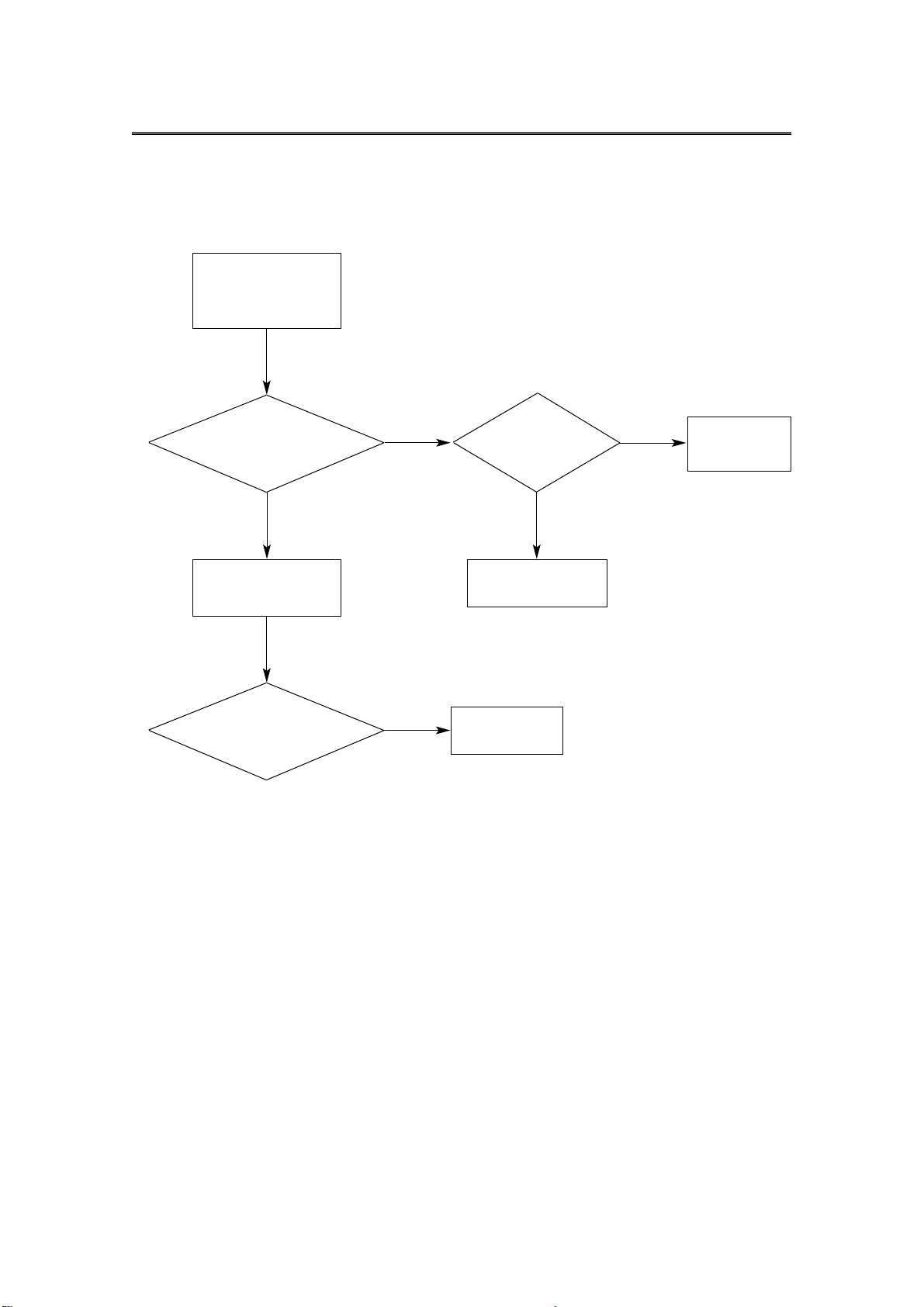
37
Appear Raster
(with Vertical
retrace line)
Check the
voltage between
+ and - C281
Check T461
D281
Check
Q901, Q902, Q903
Check Q501
Increase screen
voltage by turn right
screen volume
Readjust screen
voltage
NO
NO
NO
YES
8-2. No Raster
Heater Voltage is OK but No Raster.
Check the voltage
at pin 19, 20, 21, 26
of Q501
YES
Page 38
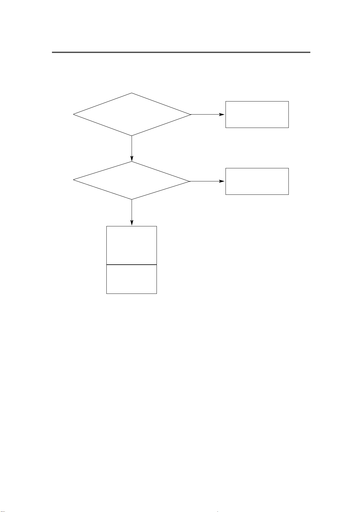
38
8-3. No Sound(Picture OK)
Do the volume control in max before check this routine.
Check the signal waveform
to the pin 2 of Q501
QS02 Check
PV05 Check
NO
Check Q501
NO
YES
Check the signal waveform
to the pin 15 of Q501
Check Voltage
at Q601 Pin 6
YES
Check Q604
Q603
Q601
W661
Page 39
39
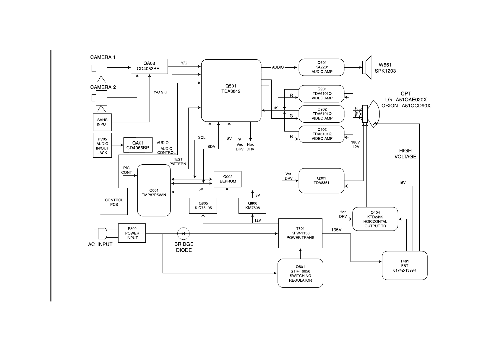
9. Block Diagram
Page 40
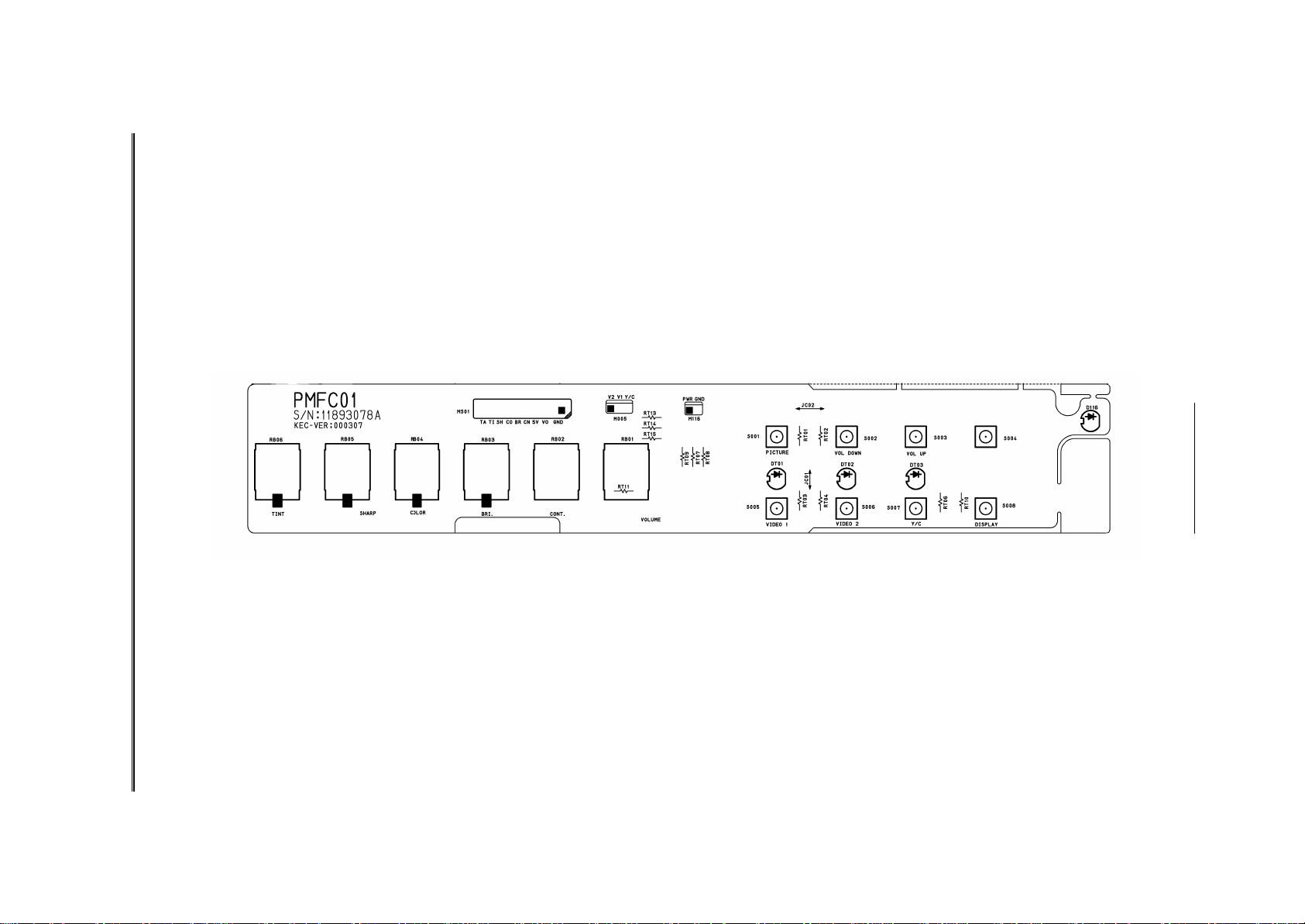
10. PCB LAYOUT (21" "F" CHASSIS)
40
Control PCB
Page 41
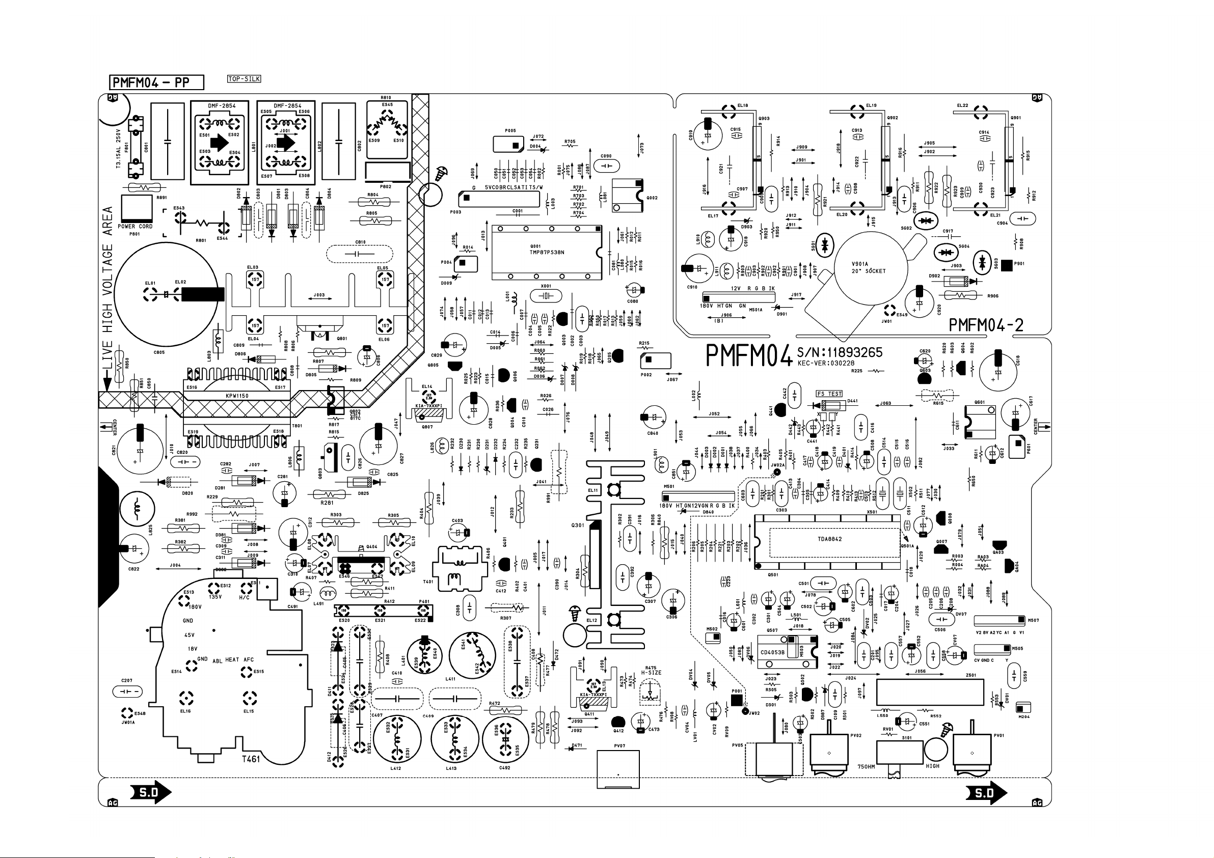
41
Page 42
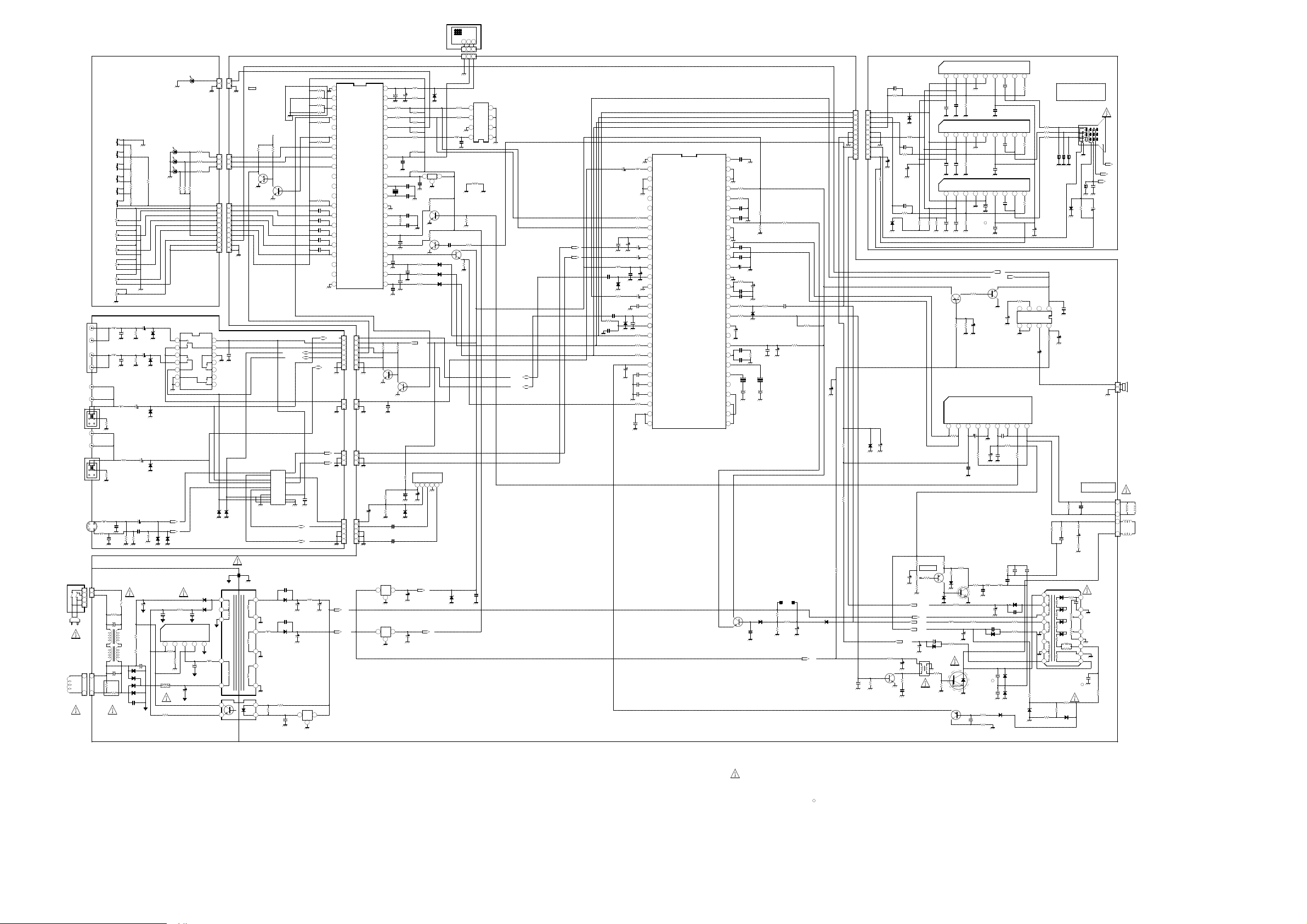
PWR S/W
SDDF3PATP011
AC CORD
123
P002
5267-03
M116
2P HARNESS
1
RT09
10K
QA01
CD4066BP
(ACTIVE HIGH)
432
C805
330uF 400V
RT15
750
RT13
750
RT14
750
C809
100pF
C810
1000p 1.6KV
3P HARNESS
MS01
10P HARNESS
VCC
D805
EU1Z
D806
EU1Z
5
L803
BFS3565
MTZ 9.1B
1
2 2
M005
1
2 2
10
9
8
7
6
5
4
3
2
1
14
13
12
11
10
9
8
DA06
C850
3300p
4kV
4
3
10
1
33
9
8
7
6
5
4
3
2
1
MTZJ 9.1B
OPTION RESISTOR
1.R701:VIDEO 2CH
2.R703: VIDEO 1CH
P004
3.R702:TACT SWITCH
5267-02
4.R704:ROTARY VR
R003
R004
P005
47K
CA03
104
Q802
H11A817C
1
2
10K
Q007
KRC112
PIN 4(LOW) : VIDEO 2 SELECT
PIN 4(HIGH) :VIDEO 1 SELECT
PIN 6(LOW) : S-VHS SELECT
PIN 6(HIGH) : VIDEO SELECT
12
13
11
10
(ACTIVE LOW)
L806
BFS3565
5267-03
P003
5267-10
5V5V
DA07
8v
CD4053BE
X0
X1
2
Y0
1
Y1
5
Z0
3
Z1
6
INH
A
B
9
C
T801
KPW-1150
R817
1K
R701
4.7K
(VIDEO 2)
R702
4.7K
(TACT)
Q008
KRC112
C054
104p
C053
104p
C052
104p
C051
104p
C050
104p
SVHS CONTROL
A/V CONTROL
QA03
14
X
15
Y
4
Z
16
VCC
7
VEE
8
GND
C
Y
C820
680pF 2KV
L825
KRFG028
D820
C821
RU3AV1
200V
100u
C825
470pF 500V
D825
C827
1000uF 25V
RGP15J
R815
15K
2
C826
104M
3
200V
GND
1
R703
10
OPT.(VIDEO)
2
OPT.(CONTROL)
3
R704 10
VIDEO SEL.
4
R705
CARS
5
4.7K
S-VHS
R001
6
4.7K
LED(SVHS)
7
LED(VIDEO 1)
8
LED(VIDEO 2)
9
V-CHK0
10
V-CHK1
11
R002
12
10K
TACT SW
13
TINT
14
SHARP
15
COLOR
16
BRIGHT
17
CONTRAST
18
TEST PATTERN
19
QUAD OPTION
20
Q001
KMP87CP38N-3UH6
VIDEO 2
11
2 2
3 3
44
5 5
VIDEO 1
CA04
104
C822
47uF 200V
1
Q803
SE135N
66
7
7
P507
M507
5267-07
7P HARNESS
2
2
P502
1
1
5267-02
P503
5267-03
Y
1
1
2
2
C
3
3
P505
5267-05
1
1
2
2
3
3
4
4
5
5
M505
5P HARNESS
+135V
+12V 1 +5V
M503
3P HARNESS
X-TAL OUT
X-TAL IN
M502
2P HARNESS
ST-BY
MUTE
V-CHK
RESET
TEST
OSD OSC
OSD OSC
BLUE
GREEN
REDGND
R552
10K
CV07
16V
100uF
KIA7808
1
KIA78L05
D116
SLG114B
DT01~DT03 : SLG114B
S006
VIDEO 2
RT06
DT01
3.9K
S007
S-VHS
RT04
DT02
2.2K
S005
VIDEO 1
S003
VOL UP
S002
VOL DOWN
S001
PICTURE
RB06
TINT
10KB
RBO5
SHARPNESS
10KB
RB04
10KB
COLOR
RB03
BRIGHT
10KB
RB02
CONTRAST
10KB
VOLUME
RB01
10KB
LA02
AUDIO
BEAD
IN 2
CA08
100pF
OUT 2
PA01
S-445-09
BNC DC-2700K
BNC DC-2700K
S103
SLIDE(2C-2P)
PV11
BNC DC-2700K
PV10
BNC DC-2700K
S102
SLIDE(2C-2P)
PV15
TCS7648-01-201
4P LARGE
S801
P881
L901
KSB-2186
LA01
AUDIO
BEAD
IN 1
CA07
100pF
OUT 1
VIDEO 2
IN
PV13
VIDEO 2
OUT
PV12
LV04
KRF9229
RV06
75
VIDEO 1
IN
VIDEO 1
OUT
LV03
KRF9229
RV02
75
LA01
S-VHS
10uH
IN
CV09
LA01
100pF
10uH
CV08
100pF
RV03
75
P805
P801
2P LARGE
F801A
3.15A
250V
R891
1M 1/2
C801
0.47uF
275V
L801
DMF-2854
L802
DMF-2854
C802
0.47uF
275V
D803
IN5398
P802
R810
2P PLUG
7 270V
2200pF 2KV
DT03
RT03
2.2K
RT02
RT05
1.3K
6.8K
RT07
RT08
10K
RT01
1.1K
CA01
1uF
RA01
220K
CA02
1uF
RA02
220K
CV10
10uF
50V
DA08
MTZJ 9.1B
CV01
50V 10uF
DA09
MTZJ 9.1B
22uF 25V
SRA
CV06
1000pF
RV04
75
C806
47uF
R805
39K
1/2R
R804
39K
1/2R
C804
2200pF 2KV
D804
IN5398
D801
IN5398
D802
IN5398
C803
10K
DA01
MTZJ 9.1B
1
2
3
4
DA02
MTZJ 9.1B
5
6
GND
7
Y
DA05
MTZJ 9.1B
C
LV02
56uH
DA04
MTZJ 9.1B
R808
2.7K
C808
820pF
Q801
STR-F6656
1
R806
1K
R807
0.24 1R
R801
1 5W
R809
4.7K
L080
10uH
VCC
42
C080
C081
100uF 10V
0.01uF
41
SDA
40
R015
R019
100
4.7K
SCL
39
R016
R018
100
4.7K
38
R017
470
37
R050 4.7K
36
IR
35
C002
1000pF
34
33
C005
15pF CH
32
X001
8.0M
31
C004
15pF CH
30
C007
12pF
29
L001
24uH
28
C006
10pF
VD
27
C015
0.022uF
HD
26
FB
25
C014
100pF
24
C013
330pF
23
2221
C012
330pF
C011
330pF
RA03
RA04
47K
10K
QA04
KRC112
QA03
KRC112
C016
470pF
L550
10uH
C557
104M
R553
10K
C558
104M
C559
104M
Q807
3
2
Q805
31
2
C552
100uF
16V
DV01
MTZJ 9.1BCV05
R013
10K
R052
4.7K
R022
10K
UGL-349KNT
1 2 3 4 5
C828
1000uF 16V
C829
470uF 16V
C003
104M
Q004
C111M
R060
100
R061
100
R062
100
VCC(8V)
Z501
COMBFILTER
D004
MTZJ
9.1B
1
3
Q003
2
KIA7042
R023
10K
Q006
C3198Y
R025
10K
Q205
C3198Y
D001
1N4148
D002
1N4148
D003
1N4148
+8v
Q002
AT24C04
R012
100
5
R011
100
L081
10uH
C010
223M
D887
MTZJ 9.1B
4
6
3
2
7
8
1
C090
104M
1
EXIT
SOUND IN
2
L601
C601
4.7uH
L002
1uH
R036
10K
R026
10K
R215
2.2K
VIDEO 2
VIDEO 1
C109
104M
C
Y
10uF
3
4
5
6
R202
220
SCL
7
R203
220
SDA
8
C301
BAND GAP
2.2uF
C302
223M
L501
10uH
C506
224M
R650
10K
C201
104M
R221
10K
C223
100pF
9
C504
2.2uF
C
10
SVHS
C505
2.2uF
Y
11
C501
C502
223M
100uF 16V
VCC
12
CVBS IN1
13
DV07
C204
1uF
MTZJ 9.1B
MTZJ 9.1B
DV02
GND
14
C602
0.47uF
AUDIO OUT
15
C503
104M
16
CVBS IN2
17
C017
100pF
BLACK CURRENT
18
18
B
19
R204
100
G
20 37
R205
100
R
21
R206
100
BEAM
22
CURRENT GUARD
R-IN
23
C208
223M
G-IN
24
C206
223M
B-IN
25
C205
223M
F/B
26
R225
1K
27
C018
100pF
Q501
TDA8842
SOUND DECC
V-DRIVE
SAND CASTLE
DIGIDEC
CVBS OUT
PLL FILTER
C603
104M
56
55
54
R201
10K
IF AGC
53
R301
39K
TOOTH
52
C303
104M
V SAW
51
EHT
50
49
48
A
47
B
46
45
GND
44
PHI-1
43
PHI-2
42
41
H-OUT
40
39
38
VCC
COLOR
36
4.43
35
3.58
34
33
32
31
30
2928
C413
1000pF
C304 1000pF
C305 1000pF
C414
4.7uF
R409
C417
472M
C419
103M
R410
18K
R413
100
C508
0.22uF
C514
104M
C513
332M
Q441
C3198Y
R403
91K
R405
1K
R401
10K
15K
C418
1uF
R414
470
C416
D401
104M
MTZJ 7.5B
R400
C512
100uF 16V
X Y
R442
1K
3k
R511
1
R441
C441
9.1K
1uF
C511
103M
R512
100K
X501
X502
4.43M
3.58M
C515
C516
240pF
220pF
D442
MTZJ 12B
R443
8.2K
C442
104M
M501
HARNESS 10P
IK
1
B
2
G
3
R
4
5
12V
6
7
8
HEAT
9
180V
C840
470uF
16V
R840
120
1/2R
R303
1 1/2R
L826
18uH
(KRF9200)
D441
1N4937
+13V
C401
390pF
1010
1
2
3
4
5
6
7
8
9
D840
MTZJ 12B
C903
56pF
R903
1.2K
D901
MTZJ7.5B
IK
B
G
R
L911
18uH
12V
C902
51pF
HEAT
C910
250V
10uF
180V
R902
1.3K
L910
18uH
C918
16V 220uF
C901
20pF
R901
1.3K
R950
2.4K
D903
MTZJ3.3B
C851
100uF 16V
R474
100K
C473
47uF 35V
470uF 35V
18V VER
R404
C403
39 1/2R
100uF
16V
Q401
C3228Y
R406
R402
1K
100
C412
222M
185V VIDEO
HEATER
45V VER
C312
1
C906
104M
1
C904
104M
1
R920
1K
R908
C905
4.7K
104M
Q604
KRA110M
R477
2.7K 1R
H-SIZE
R475
50KB
R473
10K
Q412
A1275Y
R476
100
D472
1N4148
+135V
607RA-180K
(RF9200)
C309
470pF 500V
D381
1N4937
T401
KLN2019
R411
1 1/2R
R407
27
Q231
A1266Y
Q902
(R)
TDA6111Q
2
3
4 5 6
C913
470pF
R911
2K
Q901
TDA6111Q
R912
2K
Q903
TDA6111Q
C930
1000pF
R913
2K
R620
51K
C620
10uF
Q301
TDA8351
321
C306
100u
35V
R304
1/2R
1
R472
1.2 1/2R
Q411
KTD2059Y
2.2uF 250V
R991
2R 1.0
Q404
KTD2499
HOR OUT
R234
110K
C232
104M
R235
560
500V
(G)
C914
470pF
500V
(B)
5 67879
M
AUDIO INPUT
654
C390
0.01uF
C307
C392
22uF
200V
100V
104M
L411
HW-VN
L413
KLN3041
L412
KLN3041
C492
10uF 50V NP
C281
C311
470pF 500V
D382
1N4937
C405
7500pF 1.6K
M
C406
0.1uF 630V
D232
1N4148
C908
223M
2 3 4 5 678 9
C909
223M
2 3 4
C907
223M
R602
R603
2.4K
910
R302
2.4K
C391
104M
R479
330 1/2R
R478
1K 1/2R
D471
1N4148
R281
1/2R 1
L901
C310
100V
10uF
R381
0.33 1/2R
C922
250V 104M
C923
250V 104M
C915
470pF
500V
C921
250V 104
VR
Q603
KTC3198Y
C612
16V 100uF
39 1/2R
7
R305
470pF 500V
7
0.62uF 200V
1N4937
D411
RU4DS
D412
RU4DS
8
9
R916
68K
R923
1K 1/2W
1K 1/2W
R915
68K
R914
68K
C919
250V 10uF
R611
330
2
4
3
Q601
KIA6278P
6
5
C617
16V 1000uF
98
R306
10K
KLN2061
C408
C409
0.18uF 200V
C407
0.18uF
200V
D281
C282
R992
2R 1.8
R382
0.33
1/2W
R233
8.2K 1/2R
D231
MTZJ 8.2B
V901
ORION : A51QCD90X
LG : A51QAE020X
V901A
R922
1K 1/2W
R921
SG02
R615
1R 10
L401
1
3
2
9
7
10
7
6
R232
4.7K
PCS629-03D
SG01
1.5KV
1.5KV
SG03
1.5KV
D902
1N4004
C611
1
100pF
8
C618
25V 1000uF
C308
104M
R307
220 1R
R408
1K 1/2R
C410
500V
2200pF
T461
MCG-20A36
3000
12
11
C207
0.047uF 200V
R230
16K
R231
4.7K
D230
1N4148
SG04
1.5KV
R906
2.2M
1/2W
LG : 153-210Z
ORION : ODY-S2108
L491
6800uH
C491
1uF 200V
R412
560 1/2R
H
F
S
8
4
5
M
R229
1K 1/2R
C917
2200pF 2KV
C920
4.7uF 250V
P601
5267-02
YFW500-624
H.V
FOCUS
SCREEN
W661
SPK-1203
V901L
23
P401
4P
22
21
20
-47-
CAUTION :
SINES THESE PARTS MARKED BY ARE CRITICAL FOR SAFETY USE ONES
DESCRIBED ON PARTS LIST ONLY
1.The unit of all resistors is the "OHM" unless otherwise listed.
**NOTES**
K=1,000 M=1,000,000 1/2S:SOLID 1/2W
1/2R:Metal or Metal Oxide 1/2W 5W:Cement Resistor
2.All capacitors are the 50V Ceramic ones of which the unit
is " pF" unless otherwise listed.
M
= PLASTIC CONDENSER
3.The voltage and waveform is measured between the indicated point
and the chassis ground with the DVM AND THE OSCILLSCOPE.
The input signal is a color bar one
with all picture controls at standard.
4. All diodes are the 1N4148 unless otherwise listed
PK : PEAKING COIL
CCTV SCHEMATIC DIAGRAM
MODEL NO.
CHASSIS NO. PMFM02
CPX2102MS
Page 43

THE UPDATED PARTS LIST
FOR THIS MODEL IS
AVAILABLE ON ESTA
Page 44

Hitachi, Ltd. Tokyo, Japan
International Sales Division
THE HITACHI ATAGO BUILDING,
No. 15 –12 Nishi Shinbashi, 2 – Chome,
Minato – Ku, Tokyo 105-8430, Japan.
Tel: 03 35022111
HITACHI EUROPE LTD,
Whitebrook Park
Lower Cookham Road
Maidenhead
Berkshire
SL6 8YA
UNITED KINGDOM
Tel: 01628 643000
Fax: 01628 643400
Email: [email protected]
HITACHI EUROPE GmbH
Munich Office
Dornacher Strasse 3
D-85622 Feldkirchen bei München
GERMANY
Tel: +49-89-991 80-0
Fax: +49- 89-991 80-224
Hotline: +49-180-551 25 51 (12ct/min)
Email: [email protected]
HITACHI EUROPE srl
Via Tommaso Gulli N.39, 20147
Milano, Italia
ITALY
Tel: +39 02 487861
Tel: +39 02 38073415 Servizio Clienti
Fax: +39 02 48786381/2
Email: [email protected]
HITACHI EUROPE S.A.S
Lyon Office
B.P. 45, 69671 BRON CEDEX
FRANCE
Tel: 04 72 14 29 70
Fax: 04 72 14 29 99
Email: [email protected]
HITACH EUROPE AB
Egebækgård
Egebækvej 98
DK-2850 Nærum
DENMARK
Tel: +45 43 43 6050
Fax: +45 43 60 51
Email: [email protected]
Hitachi Europe Ltd
Bergensesteenweg 421
1600 Sint- Pieters-Leeuw
BELGIUM
Tel: +32 2 363 99 01
Fax: +32 2 363 99 00
Email: [email protected]
www.hitachidigitalmedia.com
HITACHI EUROPE S.A.
364 Kifissias Ave. & 1, Delfon Str.
152 33 Chalandri
Athens
GREECE
Tel: 1-6837200
Fax: 1-6835964
Email: [email protected]
HITACHI EUROPE S.A.
Gran Via Carlos III, 101- 1
08028 Barcelona
SPAIN
Tel: 93 409 2550
Fax: 93 491 3513
Email: [email protected]
HITACHI Europe AB
Box 77 S-164 94 Kista
SWEDEN
Tel: +46 (0) 8 562 711 00
Fax: +46 (0) 8 562 711 13
Email: [email protected]
HITACHI EUROPE LTD (Norway) AB
STRANDVEIEN 18
1366 Lysaker
NORWAY
Tel: 67 5190 30
Fax: 67 5190 32
Email: [email protected]
HITACHI EUROPE AB
Neopoli / Niemenkatu 73
FIN-15140 Lahti
FINLAND
Tel : +358 3 8858 271
Fax: +358 3 8858 272
Email: [email protected]
HITACHI EUROPE LTD
Na Sychrove 975/8
101 27 Praha 10 – Bohdalec
CZECH REPUBLIC
Tel: +420 267 212 383
Fax: +420 267 212 385
Email: [email protected]
 Loading...