

Page 1

SM0401
CM771ET
CM771U
SERVICE MANUAL
CM772ET
CM772U
DJ72 Chassis
CAUTION:
FEATURES...........................................................................................................................2
SAFETY PRECAUTIONS......................................................................................................2
CHECK OF HIGH VOLTAGE HOLD DOWN CIRCUIT.........................................................2
PRODUCT SAFETY NOTICE...............................................................................................3
SPECIFICATIONS ................................................................................................................3
CONTROLS..........................................................................................................................4
SIGNAL TIMING CHART......................................................................................................5
DESCRIPTION OF CIRCUIT ................................................................................................7
TROUBLESHOOTING.........................................................................................................17
ADJUSTMENTS.................................................................................................................. 20
WIRING DIAGRAM............................................................................................................. 24
BLOCK DIAGRAM .............................................................................................................. 25
P.C.B.A. ASSEMBLY........................................................................................................... 26
REPLACEMENT PARTS LIST............................................................................................ 27
SCHEMATICS..................................................................................................................... 39
MECHANICAL PARTS LIST................................................................................................. 41
Before servicing this chassis, it is important that the service personnel must read the
“Safety Precautions” and “Product Safety Notice” in this Service Manual.
CONTENTS
H972
(V1.0)
DISPLAY ASSEMBLY.......................................................................................................... 42
ATTACHMENT A ................................................................................................................. 45
SPECIFICATIONS AND PARTS ARE SUBJECT TO CHANGE FOR IMPROVEMENT.
HIGH RESOLUTION COLOR DISPLAY MONITOR
(Sept. 2000)
Page 2
FEATURES
1. Flat screen CRT with anti-glare, dynamic focus circuit,
dark glass, and INVAR shadow mask give the
sharpest focus and highest contrast.
2. Automatic scanning and automatic adjustment to
conform to a wide range of scanning frequencies and
user requirements.
3. Signal input allows D-Sub Mini 15-pin cable.
4. Power Save Mode automatically puts the monitor into
a standby mode (power consumption less than 15W)
when the H.sync. signal is not detected, and a power off mode (less than 5W) when the V.sync. signal is not
detected. Normal mode is restored immediately when
the H. sync. signal and the V.sync. signal are detected.
This feature prolongs monitor life and reduces energy
consumption by up to about 75 %.
SAFETY PRECAUTIONS
NOTICE:
notes located on or inside the cabinet and on the chassis
or picture tube.
The following precautions must be observed.
1. Do not install, remove, or handle the picture tube in
2. When replacing a chassis in the monitor, all the
3. When service is required, observe the original lead
4 Always use the manufacturer’s replacement components.
5. Before returning a serviced monitor to the customer,
6. In the case of the microprocessor unit, shop
High Voltage
This monitor is provided with a high voltage hold down
circuit for clearly indicating that voltage has increased in
excess of a predetermined value.
Comply with notes described in this Service Manual
regarding this hold down circuit when servicing, so that
this hold down circuit may function correctly.
Comply with all cautions and safety related
any manner unless shatterproof goggles are worn.
People not so equipped should be kept away while
picture tubes are handled.
protective devices must be put back in place, such as,
barriers, non-metallic knobs, adjustment and compartment
shields, and isolation resistor-capacitor, etc.
dress. Extra precaution should be taken to assure
correct lead dress in the high voltage circuitry area.
Especially critical components as indicated on the
circuit diagram should not be replaced by other
manufacturer’s one. Furthermore where a short circuit
has occurred, replace those components that
indicate evidence of overheating.
the service personnel must thoroughly test unit to be
certain that it is completely safe to operate without
danger of electrical shock, and be sure that no
protective device built into the monitor by the
manufacturer has become defective, or inadvertently
defeated during servicing.
Therefore, the following checks should be performed
for continued protection of the customer and service
technician.
adjustment is necessary after exchange of the
microprocessor unit.
Service Warning
With minimum Brightness and Contrast the operating
high voltage in this display is lower than 30 kV.
If any component having influence on the high voltage is
replaced, confirm that the high voltage with minimum
Brightness and Contrast is lower than 30 kV.
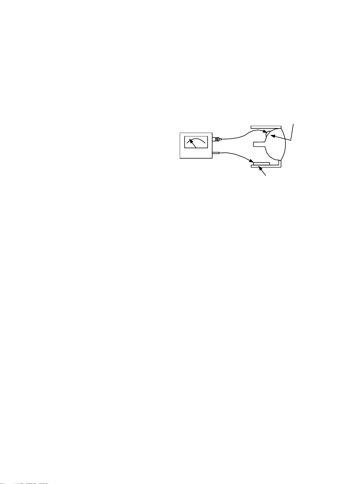
To measure high voltage use a high impedance
high-voltage meter. (SENSITIVE RESEARCH Model:
ESH or Equivalent)
Connect (-) to chassis earth and (+) to the CDT anode
button. (See the following connection diagram Fig. 1.)
NOTE:
Turn power switch off without fail before making
the connection to the Anode button
CDT ANODE
HIGH IMPEDANCE
H.V. METER
SENSITIVE RESEARCH
Model: ESH or equivalent. CHASSIS GROUND
(+)
(-)
FIG. 1
X-radiation
TUBE:
The source of X-radiation in this monitor is the
picture tube. The tube utilized in this chassis is specially
constructed to limit X-radiation emissions.
For continued X-radiation protection, the replacement
tube must be the same type as the original, manufacturer
approved type.
When troubleshooting and making test measurements in
a monitor with a problem of excessive high voltage, avoid
being unnecessarily close to the picture tube and the high
voltage components.
Do not operate the chassis longer than is necessary to
locate the cause of excessive voltage.
CHECK OF HIGH VOLTAGE HOLD DOWN
CIRCUIT
Checking of the high Voltage hold down circuit operation.
1. Turn the switch of the unit ON, and set the Brightness
and Contrast controls to max.
2. Turn the switch of the unit OFF.
3. Connect a DC Voltmeter and an adjustment jig as
shown in Fig. 2.
4. Set the adjustment VR to fully counterclockwise.
5. Turn the switch of the unit ON and gradually rotate the
adjustment VR clockwise.
6. Check that a reading of DC voltage-meter is less-than
0.60.1 V when picture disappears.
7. Turn the switch of the unit OFF immediately after
checking that the picture disappears.
8. Remove the adjusting jig and the DC voltmeter.
NOTE:
Reading of 0.6 V is approximately equivalent to
30 kV of CDT Anode High Voltage.
2
Page 3
PRODUCT SAFETY NOTICE
Many electrical mechanical parts in the color monitor
units have special safety related characteristics.
These are often not evident from visual inspection nor
can the protection afforded by them necessarily be
obtained by using replacement components rated for
higher voltage, wattage, etc. Replacement parts which
have these special safety characteristics are identified in
this Service Manual.
Electrical components having such features are identified
by marking with on the schematics and on the parts
list in this Service Manual.
The use of a substitute replacement component which
does not have the same safety characteristics as the
manufacturer recommended replacement one, shown in
the parts list in this Service Manual, may create shock,
fire, X-radiation, or other hazards.
Productions are issued from time to time. For the latest
information, always consult this Service Manual.
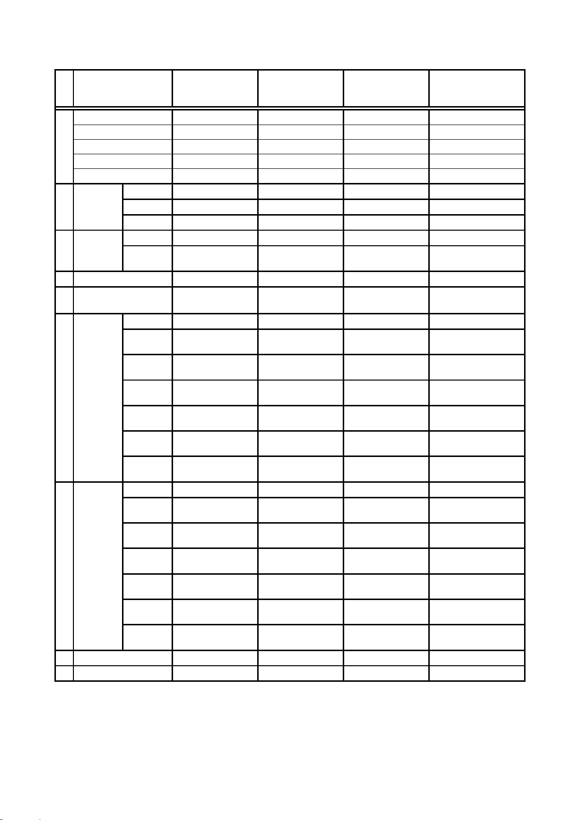
SPECIFICATIONS
DC VOLT METER
(10 V range)
VARIABLE
V
Clockwise
RESISTER
To
CHASSIS
GROUND
R793
R792
DEF BOARD ASSEMBLY
FIG. 2 CHECKING CIRCUIT USING JIG
RESISTER
300 k -B (1/2 W)
68 k (1/2W)
Model Name
CM771U CM771ET CM772U CM772ET
Destination North America Europe North America Europe
Rated Voltage AC 100-120 / 200-240 V, Automatically select.
Provided with Power Circuit.
Power Consumption 98 W nominal
Color Display Tube
(CDT)
Rated
Frequency
Resolution
Horizontal 31 - 96 kHz 31 - 96 kHz 31 - 106 kHz 31 - 106 kHz
Vertical 50 - 160 Hz
Horizontal Up to 1600 dots Up to 1600 dots Up to 1600 dots Up to 1600 dots
19 inches diagonal, 0.22 mm horizontal dot pitch,
Invar shadow mask, Black matrix, Anti-Reflection coat, Short persistence phosphors.
Vertical Up to 1280 lines Up to 1280 lines Up to 1280 lines Up to 1280 lines
Signal Inputs Red, Green and Blue analog video
H/V separate, H/V composite or Sync. on Green sync.
User Controls Power Switch
Degauss
Language Select
Contrast
Brightness
H. Position
H. Size
V. Position
V. Size
Environmental
Condition
Operation Storage
Temperature : 5 to 35 20 to 60
Rotation
Pincushion
Trapezoid
Pin.Balance
Parallelogram
H. Moiré
V. Moiré
Color Select
Red, Green, Blue
DMS Mode
OSD H-Position
OSD V-Position
Dynamic Focus
V.Linearity
V.L. Balance
Hemisphere
Total Reset
Single Recall
Top Corner Pin.
Bottom Corner Pin.
Humidity : 10 % to 80 % 10 % to 90 %
Dimensions
448(W) 442 (H) 450 (D) mm, Including Tilt & Swivel base.
Weight 24.0 kg
3
Page 4
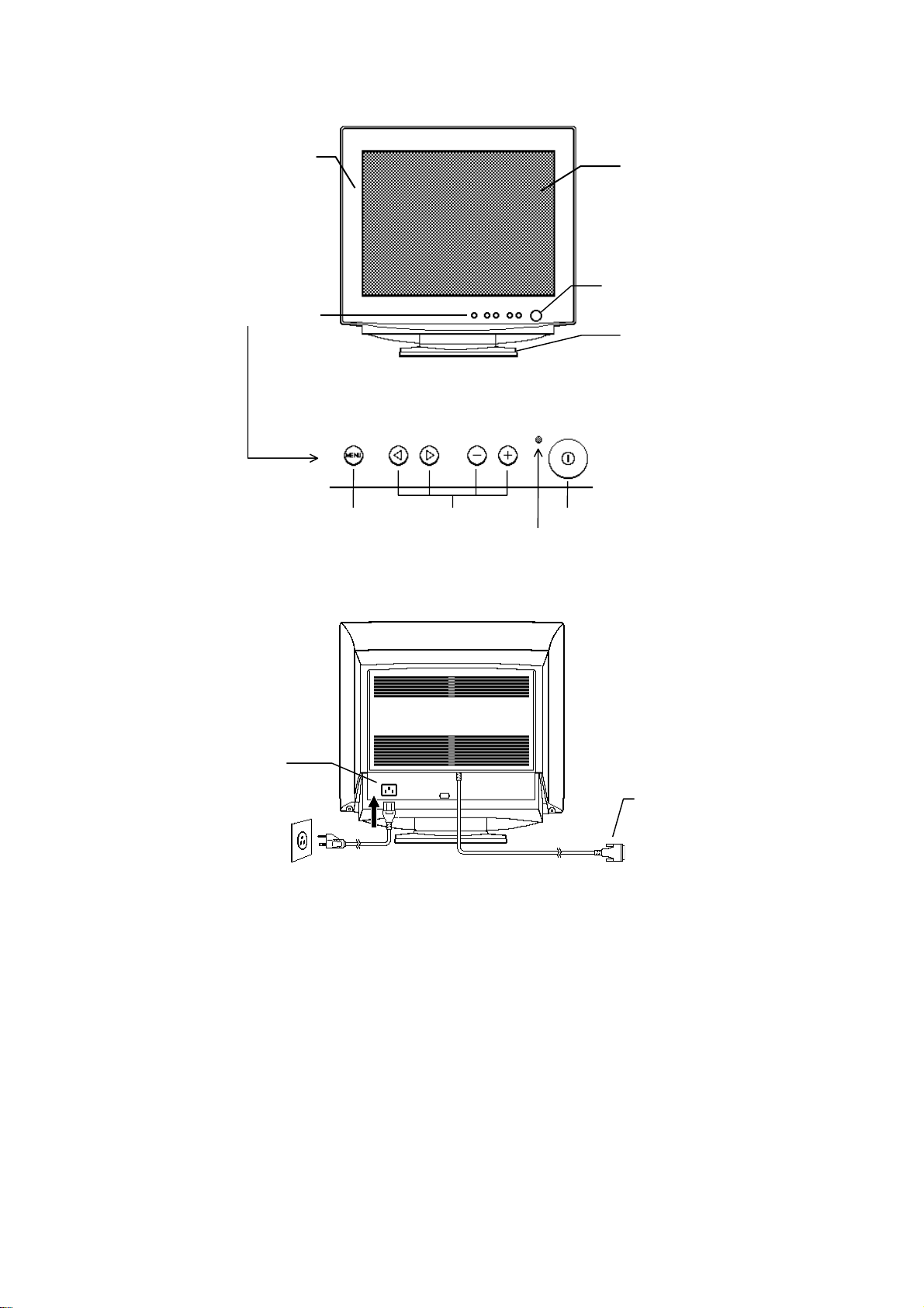
CONTROLS
Front Cover
Control Panel
FIG.3 FRONT VIEW
Menu Key Adjustment Keys
FIG. 4 CONTROL PANEL
Power Indicator
Power Switch
CRT Surface
Tilt & Swivel Base
FIG. 3 FRONT VIEW
D-Sub Mini 15-pin
AC Inlet
FIG. 5 REAR VIEW
Signal Cable
(D-Sub Mini 15-pin)
4
Page 5
SIGNAL TIMING CHART
Signal
CM771U-511 999
CM771ET-301 999
CM772U-511 999
CM772ET-301 999
1 Video Type R/G/B Analog R/G/B Analog R/G/B Analog R/G/B Analog
Voltage 0.7 Vp-p 0.7 Vp-p 0.7 Vp-p 0.7 Vp-p
Set Up None None None None
2 Sync Type H/V Separate H/V Separate H/V Separate H/V Separate
Amp. TTL Level
3 Video frequency 25.175 MHz 56.250 MHz 94.500 MHz 157.500 MHz
4 Character (Letter)
5 Horizontal Frequency 31.469 kHz 53.674 kHz 68.677 kHz 91.146 kHz
Front
porch
Sync.
width
Back
porch
Blanking
width
Display
time
H. period
(1H)
6 Vertical Frequency 70.086 Hz 85.061 Hz 84.997Hz 85.024 Hz
Front
porch
Sync.
width
Back
porch
Blanking
width
Display
time
H. period
(1H)
7 Scan System (Non-interlaced) (Non-interlaced) (Non-interlaced) (Non-interlaced)
8 Signal name 30B 54A 68A 91A
* VGA is a registered trademark of International Business Machined Corporation.
* VESA is a trademark of a nonprofit organization, Video Electronics Standard Association.
640 dots400 lines 800 dots600 lines 1024 dots768 lines 1280 dots1024
0.636 µs (16cl) 0.569 µs (32cl) 0.508 µs (48cl) 0.406 µs (64cl)
3.813 µs (96cl) 1.138 µs (64cl) 1.016 µs (96cl) 1.016 µs (160cl)
1.907 µs (48cl) 2.702 µs (152cl) 2.201 µs (208cl) 1.422 µs (224cl)
6.356 µs (160cl) 4.409 µs (248cl) 3.725 µs (352cl) 2.844 µs (448cl)
25.422 µs (640cl) 14.222 µs (800cl) 10.836 µs (1024cl) 8.127 µs (1280cl)
31.778 µs (800cl) 18.631 µs (1048cl) 14.561 µs (1376cl) 10.971 µs (1728cl)
0.381 ms (12H) 0.019 ms (1H) 0.015 ms (1H) 0.011 ms (1H)
0.064 ms (2H) 0.056 ms (3H) 0.044 ms (3H) 0.033 ms (3H)
1.112 ms (35H) 0.503 ms (27H) 0.524 ms (36H) 0.483 ms (44H)
1.557 ms (49H) 0.578 ms (31H) 0.582 ms (40H) 0.527 ms (48H)
12.711 ms (400H) 11.179 ms (600H) 11.183 ms (768H) 11.235 ms (1024H)
14.268 ms (449H) 11.756 ms (631H) 11.765 ms (808H) 11.761 ms (1072H)
VGA
640400
(70Hz)
9
9
9
9
(Neg./Pos.)
VESA
800600
(85Hz)
9999
9999
9999
9999
TTL Level
(Pos./Pos.)
VESA
1024768
(85Hz)
9999
9999
9999
9999
TTL Level
(Pos./Pos.)
VESA
12801024
(85Hz)
9999
9999
9999
9999
TTL Level
(Pos./Pos.)
lines
5
Page 6
Signal
CM771U-511
CM771ET-301
CM772U-511 -
CM772ET-301 -
1 Video Type R/G/B Analog R/G/B Analog R/G/B Analog R/G/B Analog
Voltage 0.7 Vp-p 0.7 Vp-p 0.7 Vp-p 0.7 Vp-p
Set Up None None None None
2 Type H/V Separate H/V Separate H/V Separate H/V Composite
Amp. TTL Level
3 Video frequency 202.500 MHz 229.500 MHz 25.175 MHz 24.800MHz
4 Character (Letter)
5 Horizontal Frequency 93.750 kHz 106.250 kHz 31.469 kHz 31.000 kHz
Front
porch
Sync.
width
Back
porch
Blanking
width
Display
time
H. period
(1H)
6 Vertical Frequency 75.000 Hz 85.000 Hz 59.940 Hz 50.000 Hz
Front
porch
Sync.
width
Back
porch
Blanking
width
Display
time
H. period
(1H)
7 Scan System (Non-interlaced) (Non-interlaced) (Non-interlaced) (Non-interlaced)
8 Signal name 94A 106B 30C 31W
0.316 µs (64cl) 0.279 µs (64cl) 0.636 µs (16cl) 0.403 µs (10cl)
0.948 µs (192cl) 0.837 µs (192cl) 3.813 µs (96cl) 3.790 µs (94cl)
1.501 µs (304cl) 1.325 µs (304cl) 1.907 µs (48cl) 2.258 µs (56cl)
2.765 µs (560cl) 2.440 µs (560cl) 6.356 µs (160cl) 6.452 µs (160cl)
7.901 µs (1600cl) 6.972 µs (1600cl) 25.422 µs (640cl) 25.806 µs (640cl)
10.667 µs (2160cl) 9.412 µs (2160cl) 31.778 µs (800cl) 32.258 µs (800cl)
0.011 ms (1H) 0.009 ms (1H) 0.381 ms (10H) 3.548 ms (110H)
0.032 ms (3H) 0.028 ms (3H) 0.064 ms (2H) 0.129 ms (4H)
0.491 ms (46H) 0.433 ms (46H) 1.049 ms (33H) 3.097 ms (96H)
0.533 ms (50H) 0.471 ms (50H) 1.430 ms (45H) 6.774 ms (210H)
12.800 ms (1200H) 11.294 ms (1200H) 15.253 ms (480H) 13.226 ms (410H)
13.333 ms (1250H) 13.333 ms (1250H) 16.683 ms (525H) 20.000 ms (620H)
VESA
16001200
(75Hz)
9
9
(Pos./Pos.)
1600 dots1200
lines
VESA
16001200
(85Hz)
-
-
9
9
TTL Level
(Pos./Pos.)
1600 dots1200
lines
VGA
640480
(60Hz)
TTL Level
(Neg./Neg.)
640 dots480 lines 640 dots410 lines
TTL Level (Neg./Neg.)
Adjustment
signal
6
Page 7

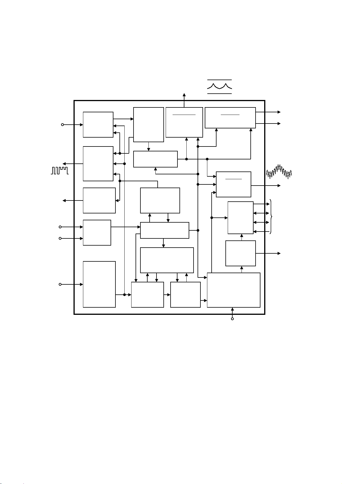
DESCRIPTION OF CIRCUIT
1. Power Supply Circuit
This model incorporates a wide range universal power supply utilizing a switching regulator (see block diagram in Fig.6).
1.1 AC input
AC input consists of AC inlet, EMI filter (C901C905,C907) and rectifier (D901D904). Rectifier circuits adapt to
full-wave method. Inrush current limiting circuit (R90A) protects from excessive inrush current at initial stage of power
on.
1.2 Switching Regulator circuit
Switching Regulator circuit is designed to handle variations of two conditions to ensure constant +B voltage to
secondary circuit : (Circuit #2) varying load conditions of video, (Circuit #3) varying horizontal frequencies and load
conditions.
1.2.1 Circuit #1 :
Circuit #1 consists of chopper inductor (L910), chopper component (Q910), rectifier component (D910, C920) and
control IC (I920). R918 and R919, R91A detect output voltage and provide signal to I920 pin 20 which adjusts the pulse
width based on the pin 20 voltage level to provide constant voltage output.
1.2.2 Circuit #2 :
Circuit #2 consists of chopper transformer (T921), chopper component (Q920) and control IC (I920). T921 detects
output voltage and provides signal to I920 pin 4 which adjusts the pulse width based on the pin 4 voltage level to provide
constant voltage output. If the secondary circuit becomes overloaded, primary current through T921 is detected at R923,
R924 and stops the switching operation. Once the circuit has overloaded, the power switch must be turned off for a
short period and then turned on to re-establish power.
Switching frequency is determined by time constant of R92E and R92F, R92G.
1.2.3 Circuit #3 :
Circuit #3 has two outputs. +5V is used mainly to drive the microprocessor circuit and input the signal selection circuit.
+6.3V is used for the CRT heater.
When the DC voltage from circuit #1 is applied to I940, I940 starts oscillations. Once oscillations start, the switching
transistor is driven by the voltage taken from the tertiary winding of T940. The output voltage of the T940’s tertiary
winding is rectified by D942 and C942.
The main power supply (Circuit #2) turns on (off) when a signal High (Low) is applied to the base of Q984 from the
microprocessor circuit.
1.3 Degaussing circuit
When the power is switched on, the CRT is degaussed automatically by current flowing through the degauss circuit
while the relay (S99R) is closed. Degaussing current flows for approximately 20 seconds and stops by causing relay
(S99R) to be opened after secondary circuit operation is stabilized.
The circuit also allows for manual degauss by using “DEGAUSS” control on OSD menu which closes S99R through
Q991 to allow current to flow through the degauss coil.
7
Page 8
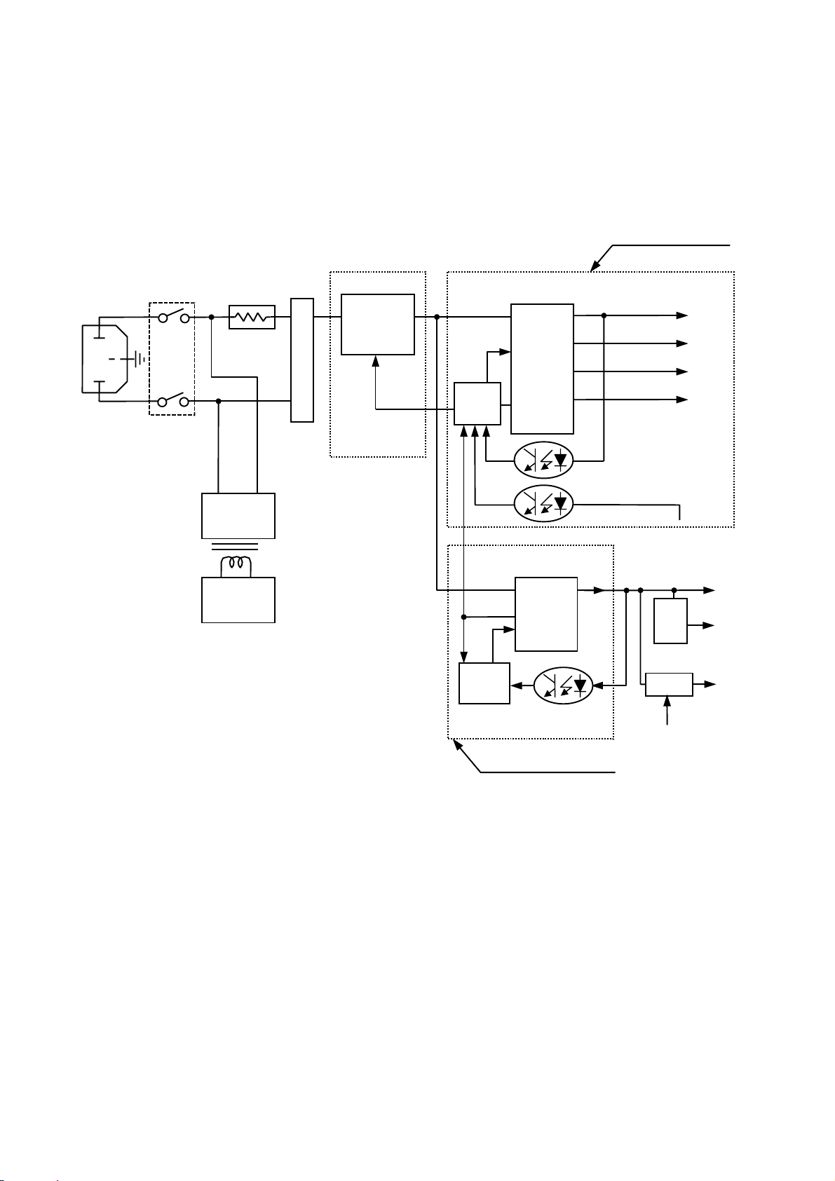
AC inlet
FIG. 6 BLOCK DIAGRAM FOR POWER SUPPLY CIRCUIT
Main power supply
Circuit #2
Chopper
Chopper
Control
+B
+85V
+54V
+14V
Circuit #1
Degauss
Circuit
Manual
Degauss
Circuit #3
+ 12V
Chopper
On/Off
control
5V
Reg.
+ 6.3V
MPU
Control
Standby power supply
On/Off
On/Off
control
Heater
8
Page 9
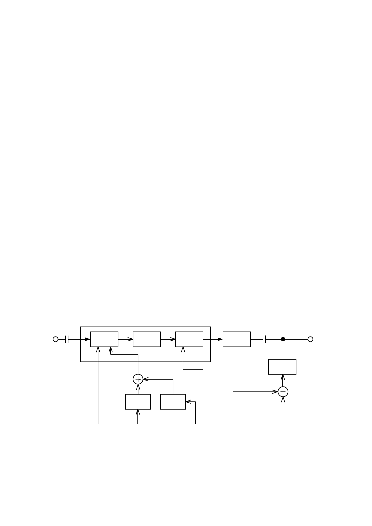
2. Video Processing Circuit
Amp
p
2.1 Video select circuit (Optional)
Two of Video input signals shall be switched at Video selector (I205) controlled by switching signal coming from
microprocessor.
2.2 Video Processor
The video input signal of 0.7 Vp-p is amplified to approximately 50 Vp-p by the video processing circuit and is fed to the
cathode to drive the beam current.
This chassis incorporates a single chip video processor I201, with three channels, one for each of R/G/B, which
functions as the pre-amp of the inputs, OSD mixer and also gain control. A control signal from the microprocessor
changes the amplifier gain of the video channels (R/G/B) together with white balance control.
Video Output circuit I202 amplifies R/G/B signals controlled by I201 to the enough level to drive Cathode of CRT. DC
voltage of Cathode is determined by DC Cut off voltage from Cathode Clamp Circuit. DC Cut off voltage is generated at
Level Shift Circuit which consists of I203, Q22R, Q22G and Q22B, whose R/G/B channels are also controlled by
microprocessor.
2.3 ACL Circuit
The current at the secondary winding of the flyback transformer is used to represent the CRT beam current. The current
is measured and fed to the contrast control Q281,Q282 to limit the maximum beam current with negative feedback.
2.4 Blanking Circuit
Video blanking during the beam retrace period is achieved by applying both horizontal and vertical blanking pulses to
I201.
2.5 Precedence of Clamp Pulse Circuit
Video Processor I201 receives Clamp pulse signal from I701, Precedence of Clamp Pulse Circuit.
2.6 OSD Circuit
I301 receives H/V pulses from Deflection Circuit and control signal from microprocessor, whose output feeds Clock
signals synchronized with H pulse and control signals from microprocessor, OSD display signals in R/G/B, OSD
blanking signal to OSD Mixer Circuit in I201.
FIG. 7 VIDEO PROCESS CIRCUIT
Video in to CRT
Video Processor I201
Gain
Control
Amp. Clamp
Level
shift
ACL
I701
Output
.
Cathode
clam
Cathode
R/G/B Gain
Control
Contrast
Control
From FBT
Brightness
Control
R/G/B Cut off
Control
9
Page 10
)
8Buffe
e
t
)
3. Horizontal Deflection and High Voltage Regulation Circuit
3.1 Horizontal Deflection Circuit
The purpose of the horizontal deflection circuit is to cause the CRT electron beam to be scanned horizontally by driving
a current through the deflection yoke, synchronized by the H sync pulse. The circuit consists of an AFC circuit, made up
of an H phase locked loop and VCO (voltage controlled oscillator), and the deflection output.
The H.sync. signal is input to I701 where it is delayed and then input to a phase detector. The phase locked loop (I701)
also accepts input from a saw tooth waveform which is provided by the deflection feedback (flyback pulse) through the
R707. The output of the phase detector creates an error voltage between the feedback pulse and the input pulse and is
then fed to the VCO after processing by an AFC Filter.
If the oscillator frequency deviates more than 4% of H.SYNC, PLL1 (I701) goes into search mode and HUNLOCK (I701)
changes to “H”. The minimum horizontal frequency is determined by the capacitor at C706 and R704. Horizontal
frequency range is determined by R705. H.SIZE, S.PIN and Trapezium are controlled by PWM circuit (Q801). The
output pulse from the VCO is fed to the pre-drive and then output from I701 to the drive buffer Q701 / Q702. The
pre-drive circuit within I701 is controlled by duty cycle by the internal circuit.
In case of no sync signals supplied or excessive frequency change, such as a signal timing change, HUNLOCK once
changes to “H”, and PWM circuit (Q801) output is stopped.
The deflection circuit of the DJ72 chassis has been separated from the high voltage regulation circuit to provide
improved H linearity performance by utilizing the consonant conditions of the horizontal beam current characteristics.
The S-consonant capacitors, C770C777, are changed by Q767Q771 and S77R, which provide 812 stages of
consonant conditions. The horizontal linearity coils L771L772 are changed by S77R to provide two stages of H
Linearity conditions.
The H.DEF +B voltage chopper power supply parabolically modulates the H.DEF +B voltage of the deflection circuit,
based on the horizontal frequency, to provide a frequency - dependent voltage of between 42.5V and 160V to the
deflection circuit.
HFLB
V.SYNC
H.CP
V.BLK
From MPU
H.SYNC/Composite SYNC
MPU
FIG. 8 HORIZONTAL DEFLECTION CIRCUIT
I701
14
SEPA
RATER
SDA
SCL
+B (+200V
16
19
18
15
17
H.SIZE CONTROL
OSCILLATOR
5 3 4 6
Drive
Buffer
E / W
From
H.SIZE
PWM
H.Cen
MPU
32
12
13
I601
Vertical
Output
f
H-V
Def
Out
Amp
Amp
Driv
r
H.DRIVER
+B E
V.DY
Lin.
Coil
(85V
PWM
E
HV
Module
Lin.
Coil
T751
T751
L771
ERROR
S77R
C771~
Q767~
Q771
10
C777
From MPU
S.fig.
Cap.
S.fig.
Cap.
C770
From MPU
Select Select
Page 11
V-sync
clamping
blanking
HUNLOCK
SDA
SCL
I701
14
16
17
19
18
FIG. 9 DEFLECTION CONTROL IC BLOCK DIAGRAM
EWDRV
11
EW-Output
H-Pincushion
H-Corner
H-Trapezium
-
V-Sync
Integrator
Video
Clamping
And
V-BLANK
HUNLOCK
Output
I2C-BUS
Receiver
Vertical
Oscillator
and AGC
V-Position
V-Size,VOVSCN
Protection
and Soft Start
I2C-BUS Registers
7V
1.2V
V-Output
V-Linearity
V-Linearity Balance
FOCUS
Horizontal
and Vertical
H-Size
Control
12
13
32
6
4
3
5
V
OUT2
V
OUT1
Focus
H-Size
Control
Oscillator
H/C-sync
15
H/C-Sync
Input and
Polarity
Correction
Coincidence
Detector
PLL1 and
H-Position
Horizontal
Oscillator
H-Output
Stage
PLL2,Parallelogram,
Pin Unbalance and
Soft Start
1
HFLB
HDRV
8
11
Page 12
FBT
3.2 High Voltage Regulation Circuit
The output pulse from Q701 is also fed to the high voltage regulation circuit with the same design of consonant circuit as
the horizontal deflection circuit. High voltage of 27.0 kV is obtained by the step-up windings of the flyback transformer to
drive the CRT anode. The high voltage is monitored by the E
error detection circuit. The error detection circuit
HV
functions by stepping the high voltage down and comparing it with the reference voltage of inside I740 whose output
controls I740, the Integrated Circuit included with E
switching transistor.
HV
3.3 Dynamic focus drive circuit
This monitor’s CRT includes a dynamic focusing electron gun to achieve sharp and uniform focus throughout the display
area. The CRT’s Focus anode receives a DC component of approximately 27% of the CRT anode voltage, combined
with the AC voltage parabolic wave form of magnitude of 600 Vp-p horizontal, and 180 Vp-p vertical. DC focus voltage is
obtained from a tap of the flyback transformer’s bleeder resister, and fed to G3 focus electrode. Horizontal and vertical
parabolic output pulses are amplified at Q501Q508, T560 and fed to the flyback transformer where they are combined
with the DC component (27% of anode voltage). The potentiometers (focus 1, focus 2) at the flyback adjust the DC
focus voltage. The focus 2 potentiometer mainly adjusts horizontal beam shape (vertical line width), and the focus 2
potentiometer mainly adjusts the vertical beam shape (horizontal line width) by optimizing the DC component of the
parabolic waveform.
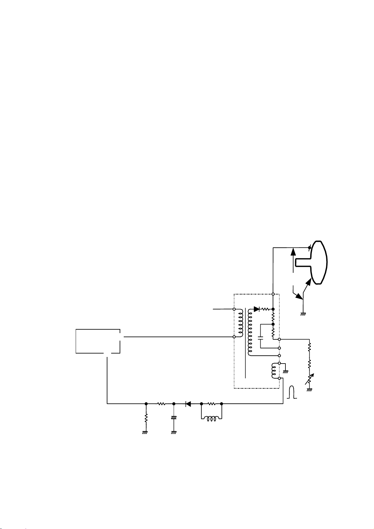
3.4 High Voltage Hold-Down Circuit
DJ72- Chassis uses a system that stops H/V DRIVE SIGNAL output when abnormal high voltage is detected. So that
the high voltage output will be declined to zero. The circuit operation in detail is as follows.
When an input voltage to I740 (pin15, it is determined by R792 and R793) exceeds the specified level, the high voltage
is declined to zero.
FIG.10 HIGH VOLTAGE HOLD-DOWN CIRCUIT DIAGRAM
For the models CM771U-511, CM771ET-301
8
10
E
HV
I740
module
EHV +B
R792 R791
R793
+
C791
-
D790
L791
HIGH
VOLTAGE
CRT
R746
R756
R747
12
Page 13

4. Vertical Deflection Circuit
The purpose of the vertical deflection circuit is to cause the CRT electron beam to be scanned vertically by driving a
current through the deflection yoke, synchronized by the V sync pulse. V sync is input to the V oscillator circuit, I701,
generating the vertical saw tooth wave. The vertical saw tooth wave is fed to I601 to be amplified of I601 to drive the
vertical deflection yoke.
The feedback circuit inside I601 works such that the differential voltage between pin9 and pin4 equals zero. The
differential input current is compared with the feedback current, and the differential drives the output amplifiers. By
varying resistor R612 or R619 one can set the desired deflection current.
The picture can be shifted in vertical direction by making a DC-offset current through the coil. DC-offset current through
the coil is controlled by the differential input current from I701.
I601 uses an external flyback supply voltage, which is connected to pin7. The signal from the I601 8pin output is used
for protection. The guard output is also activated during thermal shutdown i.e. when Tj>=160
of range.
FIG. 11 VERTICAL DEFLECTION CIRCUIT
o
C, and feedback loop out
V.SYNC
From MPU
SDA
SCL
V.BLK
I601
8 3 5 7
GUARD
I701
V.Lin
V.Lin balance
V.Position
19
18
13
12
V.OUT
14
IN A
IN B
1
INPUT
STAGE
2
CIRCUIT
PROTEC
TION
GND
C609
+
AMPLIFIER
AMPLIFIER
V
VP
FB
+
C613
FLYBACK
GENERATOR
A
B
6
OUT A
9
FEEDB
4
OUT B
C610
R620
R619
R611
V.DY
R612
13
Page 14

5. Microprocessor Circuit
The microprocessor circuit consists of the following four detailed circuits as shown in Fig.12.
1. Sync detect circuit
2. Front panel key data Input / Output (I/O)
3. Processing and memory
4. Control output
5.1 Sync detect circuit
The sync priority selector (I302) outputs H/V separate or composite sync signal to the sync processor inside the
microprocessor (I101). The sync processor has H/V polarity detector and sync separator for composite sync, H/V
frequency counter, dummy frequency generator, and outputs the processed H/V sync signal to the deflection processing
IC (I701) through the sync selector (I104).
5.2 Front panel key data Input / Output (I/O)
Microprocessor (I101) received user input from the front panel keys, which consists of: one menu key, four adjustment
keys (two pairs)
Contrast and Brightness are adjusted by four adjustment keys when OSD is disappeared.
Other feature requires controlling four adjustment keys when OSD is appeared by a menu key.
Current settings (including picture size, geometry, and color setting) are automatically stored to non-volatile memory.
The maximum memory capacity is for 48 presets including factory standard settings.
5.3 Processing and memory
I101 is an 8-bit microprocessor that equips with ROM and RAM for system program and sync processing circuit. Data
memory consists of one EEPROM chip (I102) for preset data.
5.4 Control output
Output of the microprocessor (I101) controls the deflection processing IC (I701) and the video pre-amplifier IC (I201),
the OSD control IC (I301), the rotation circuit, Horizontal drive correction circuit, the mute circuit, the sync priority
selector (I302), sync selector (I104), power save function. The deflection processing IC receives the signal through I
Bus to control the geometric function (H/V size and position, Pincushion, Trapezoid, Pin.Balance, Parallelogram, H/V
Moiré, Dynamic focus, Top/Bottom corner pincushion, V.Linearity, V.L.Balance). The video pre-amplifier IC receives the
signal through I
to control R/G/B Cut off and Contrast, Brightness, Sub BKG, ACL, C-Contrast, and shows guidance for monitor control
function on screen display by generating video signal for OSD and feeding it to video pre-amplifier IC. Power save
function has Standby mode (main power supply has no output if either H sync or V sync is not supplied) and Off mode
(all power supply except +5V have no output if both H sync and V sync are not supplied). The mute circuit brings video
output to black level when timing signal changes or the monitor goes into the power saving mode.
This chassis is capable of communication with external PC for factory adjustment through video connector (D-sub).
2
C Bus to control R/G/B Gain and Sub Contrast. The OSD control IC receives the signal through I2C Bus
2
C
14
Page 15

y
Sync on Green
H/V Separate
or
Composite Sync
FIG. 12 MICROPROCESSOR CIRCUIT
Sync
Priority
Control
Polarity
H/V s
Detect
nc
H/V sync
H.sync
H/V sync
H/V
Dummy
Sync
Generator
Selector
Deflection
1.H/V Size
2.H/V Position
3.Pincushon
4.Trapezoid
5.Pin.Balance
6.Parallelogram
7.Top/Bottom corner Pin.
OSD
8.H/V
9.Dynamic Focus
10.V.Linearity
11.V.L.Balance
12.Hemisphere
1.Contrast
2.Brightness
3.Color BKG R/G/B
4.Sub BKG
5.C-Contrast
6.ACL
Moiré
Front
Keys
Video
V Sync
Separator
DDC
port
V.sync
Sync Processor
Central
Processing
Unit
ROM RAM
H/V
Frequency
Counter
DAC
I101
I102
EEPROM
Microprocessor Circuit
I2C BUS
Video
Mute
Freq.
Select
Power
Save
Function
Rotation Control
Horizontal
drive
correction
1.Color Gain R/G/B
1.S-Fig. Cap select
1.Main power supply
On/Off
2.CRT heater
On/Off
1.H.SIZEC
2.f
to V
H
15
Page 16

6. Power Save Function
The DJ72 chassis is capable of power savings by sensing of the sync input conditions by the microprocessor. The
microprocessor can identify two sync conditions, (1) No detection of H.sync, (2) No detection of V sync.
The following table shows the details of the Power save mode.
TABLE: POWER SAVE FUNCTION
Sync
V Sync Yes Yes No No
VESA
Standard
Effect None Minimum Minimum Maximum
Circuit
Operation
Video
Power LED CM771U-511
Power consumption
(Typical) : AC (120V)
H Sync Yes No Yes No
Name Normal Standby Suspend Off
Recovery Time N/A Short Short
H. Deflection
V. Deflection
CM771ET-301
Normal
operation
Normal
operation
Normal
operation
Lighting
Green
All White : 98W
All Black : 65W
System
Dependent
Stop Stop Stop
Stop Stop Stop
Mute Mute Mute
Lighting
Orenge
less than 10W less than 10W less than 3W
Lighting
Orenge
Lighting
Orenge
16
Page 17

TROUBLESHOOTING
1. Raster does not appear
Relevant circuit : Power circuit, Horizontal deflection circuit,
High voltage limitter circuit
Check supply
Voltage AC100-200V/
AC 200-240V
Normal
Check F901
Power LED is green.
Normal
(Normal)
Yes
Abnormal
Abnormal
(Abnormal)
No
Replace F901
The power LED
is orange.
Normal
Ye s
Abnormal
No
Trouble outside the monitor
Q910, Q902, I940
D901, D902, D903, D904
C901, C902, C903, C904,
C905, C907, C910, C920
(Change the DJ72 Main Board)
I940, D98A
(Change the DJ72 Main Board)
Horizontal drive pulse
Abnormal
Normal
Check +B
after removing
L971
193.5+
3 V
Others
Sync. Signal input error
Refer to Item 2.
(Change the DJ72 Main Board)
Q765, Q801, I740
(Change the DJ72 Main Board)
(Change the DJ72 Main Board)
Sync. Signal input error
Refer to Item 2.
I740, T751
17
Page 18

2. Synvhronization is not obtained
Relevant circuit : Sync. input circuit, Microprocessor, Deflection circuit
H.SYNC and V.SYNC of
H.SYNC and V.SYNC of
Check
I101 8pin and 9pin
normal
Check
I701 15pin and 14pin
normal
abnormal
abnormal
H.Sync.
or
V.Sy nc .
V.SYNC is
not
obtained
3. Vertical single line
Relevant circuit : Horizontal output circuit
H.SYNC is
not
obtained
I101, I104, I201, I302
Q320, D26Z, D35Z
(Change the DJ72 Video
Board or Main Board)
I101, I104, I201, I302, Q320
D19Z, D27Z, D36Z
(Change the DJ72 Video
Board or Main Board)
I104,I701
(Change the DJ72 Main
Board)
I101,I701
(Change the DJ72 Main
Board)
DY faulty, Q801, D763, Q764, Q765
4. Horizontal single line
Relevant circuit : Vertical deflection circuit
Check the
voltage on pin 3 of
voltage on pin 7 of
voltage on pin 24 of
I601
13~15V
Check the
I601
53~56V
Check the
I701
Normal
Others
Others
Vertical sawtooth is
not obtained
DY, C974, D764, D975, I601,
I971, Q763, Q764
(Change the DJ72 Main Board)
C973, D604, D605, D974,
I601, R610
(Change the DJ72 Main Board)
I701
(Change the DJ72 Main Board)
C602, C603, C621, I601,
R603, R604, R621, R622
(Change the DJ72 Main Board)
18
Page 19

5. Color does not appear
A
Relevant circuit : Video amplifier circuit
Check
the input signal.
Normal
Check
the voltage of 12V
Normal (12V)
Check the
voltage of I201
24 pin
Normal (1.5~4.0V)
Abnormal
Abnormal
0V
the voltage of I201
Check
18 pin
Abnormal
Normal (2~3V)
Trouble outside the
character monitor
D975, I971
(Change the DJ72 Main Board)
bnormal
Check the
voltage of I301
13 pin
Normal (0~5V)
I301, I101
I203, Q281, Q282
Check
the voltage of I202
1 pin
Normal (30~75V)
Note
: Trouble in the blue circuit is shown in this diagram as representative color.
Refer to : when green does not appear, and when red does not appear.
0V
(Change the DJ72 Video Board)
I201,I101
(Change the DJ72 Video Board)
I202
(Change the DJ72 Video Board)
I203, Q22B
(Change the DJ72 Video Board)
19
Page 20

ADJUSTMENTS
1. Power supply
1.1 Standby power supply voltage adjustment.
(1) Turn the switch of the unit off.
(2) Place a jumper wire across R943, Q801 (G)-(S), I101(26pin) to GND, I740(13pin) to GND on main-p.w.b to
disable Main power supply voltage.
(3) Place resister 3.9k(31W) across C971(+) to GND
(4) Receive reverse cross hatch pattern of signal 94A.
(5) Connect a Digital multimeter across C981.
(6) Turn the switch of the unit on.
(7) Adjust Standby power voltage to 6.2 0.05V using R982.
(8) Turn the switch of the unit off.
(9) Remove the jumper wire.
1.2 PFC output voltage adjustment.
(1) Turn the switch of the unit off.
(2) Place a jumper wire across Q801 (G)-(S), I101(26pin) to GND, I740(13pin) to GND on main-p.w.b to disable
horizontal output and EHV output.
(3) Place resister 3.9k(31W) across C971(+) to GND
(4) Receive normal cross hatch pattern of signal 94A.
(5) Connect a Digital multimeter between + and - of C920.
(6) Turn the switch of the unit on.
(7) Adjust R919 to 364 2V.
(8) Turn the switch of the unit off.
(9) Remove the jumper wire.
1.3 Main power supply voltage adjustment.
(1) Turn the switch of the unit off.
(2) Place a jumper wire across Q801 (G)-(S), I101(26pin) to GND, I740(13pin) to GND on main-p.w.b to disable
horizontal output and EHV output.
(3) Place resister 3.9k(31W) across C971(+) to GND
(4) Receive reverse cross hatch pattern of signal 94A.
(5) Connect a Digital multimeter across C972.
(6) Turn the switch of the unit on.
(7) Adjust Main power supply voltage to 85.5 0.3V using R973.
(8) Turn the switch of the unit off.
(9) Remove the jumper wire.
20
Page 21

2. Deflection circuit
2.1 SUB H.SIZE adjustment
(1) Turn the switch of the unit off.
(2) Connect a Digital multimeter across C771.
(3) Turn the switch of the unit on.
(4) Receive normal cross hatch pattern of signal 94A.
(5) Adjust H.SIZE to maximum and S.Pincushion minimum by the Front Key.
(6) Adjust R811 to the C771 voltage value to 130 0.5V.
(7) Receive normal cross hatch pattern of signal 30C and check the C771 voltage is at 42.5 1.5V.
adjustment
2.2 High voltage adjustment
(1) Turn the switch of the unit off.
(2) Connect a high voltage meter, which is capable to measure up to 40kV, between CDT anode and GND.
(3) Receive normal cross hatch pattern of 94A signal.
(4) Turn the switch of the unit on.
(5) Adjust high voltage level to 27.0 0.3kV using R747.
(6) Turn the switch of the unit off.
(7) Remove the adjustment jig.
21
Page 22

3. Video circuit
Prior to the video circuit adjustment, all sync. and Deflection circuit adjustment must be completed. The monitor must
have been warmed up for more than 60 minutes. Video signal must be terminated with 75 and should provide the
correct voltage at the monitor end.
[Pre-setting before adjustment]
TABLE 3: OUTPUT OF DAC
Function Pin No. Output
R Color FF (MAX)
G Color FF (MAX)
B. Color FF (MAX)
R. BKG #16 pin (I301) 0V (MIN)
G. BKG #17 pin (I301) 2.5V (CENT)
B. BKG #15 pin (I301) 0V (MIN)
Contrast #13 pin (I301) 0V (MAX)
Brightness #18 pin (I301) FF (MAX)
Sub Contrast 7F (CENT)
Sub Brightness #11 pin (I301) 7F (CENT)
ACL #12 pin (I301) 7F (CENT)
C-Cont #14 pin (I301) FF (MAX)
Note 1) Color Analyzer : Minolta CA 100 or equivalent.
3.1 Cut off adjustment
(1) Receive a signal of 94A with a blank signal pattern. (Black video)
(2) Connect a high impedance voltmeter (more than 1000M) to the Screen terminal (G2) on the Video board.
Adjust the Screen voltage pot on FBT to see 600 5V .
(3) After the screen voltage adjustment is completed, fix the SCREEN VR(FBT) shown in Attachment A.
(4) Ambient light on the surface of the CRT should show lower than 20 lux.
(5) Adjust R, G & B, BKG to show the CIE coordinate of
X=0.3130.02, Y=0.3290.02 at 1.2 cd/m
2
(0.35ft-L).
If it looks difficult to obtain X and Y readings mentioned above, do the followings to obtain these numbers.
1) Reset Sub Brightness to 9Fh or 60h.
2) Reset Sub Brightness to CFh or 30h.
3) If the adjustment can not be done with 1) and 2).
When the value shown below can not hight: Change the R827 to R82E.
When the value shown below can not low: Change the R827 to R82D.
3.2 White balance adjustment (Color 2)
(1) Receive a signal of 94A with a 100100 mm window pattern.
(2) Set Brightness Control to the center (7Fh) and C-Cont to the minimum (00h).
(3) Adjust the light output to 80 cd/m
(4) Adjust the white balance of high light output by Green and Blue color adjustments to read CIE coordinate of
X=0.313 0.008, Y=0.329 0.008
(5) Adjust Contrast Control to read 3 cd/m
(6) Adjust Red and Blue BKG to read the same CIE coordinate shown in 3.2.(4)
(7) Adjust Contrast or Sub Contrast Control to read 80 cd/m
shown out range, go back to 3.2(4)
(8) Register the readings of R/G/B BKG and Color data (Color 2) to the microprocessor.
2
(24.6ft-L) at the center of screen by adjusting Sub Contrast Control.
2
(0.87ft-L).
2
(23.3ft-L) and then confirm CIE coordinate. If it
3.3 White balance adj
ustment (Color 1)
(1) Receive a signal of 94A with a 100100 mm window pattern.
(2) Set Brightness Control to the center (7Fh) and C-Cont to the minimum (00h).
2
(3) Adjust the light output to 80 cd/m
(23.3ft-L) at the center of screen by adjusting Sub Contrast Control in
Color 2 mode.
(4) Adjust the white balance of high light output by R/G/B color adjustments to read CIE coordinate of
22
Page 23

X=0.281 0.008, Y=0.311 0.008
(Either Red color or Green color must be set to the maximum (FFh) )
(5) Register the readings of R/G/B BKG and Color dada (Color 1) to the microprocessor.
3.4 White balance adjustment (Color 3)
(1) Receive a signal of 94A with a 100100 mm window pattern.
(2) Set Brightness Control to the center (7Fh) and C-Cont to the minimum (00h).
2
(3) Adjust the light output to 80 cd/m
(23.3ft-L) at the center of screen by adjusting Sub Contrast Control in
Color 2 mode.
(4) Set Red color to the maximum (FFh).
(5) Adjust the white balance of high light output by Green and Blue color adjustments to read CIE coordinate of
X=0.336 0.008, Y=0.352 0.008
(6) Register the readings of R/G/B BKG and Color data (Color 3) to the microprocessor.
3.5 White balance adjustment (DMS)
(1) Register Color 1 data(R/G/B BKG and Color data) to the microprocessor as DMS Color data.
3.6 Brightness adjustment
(1) White balance adjustment must have been done before Brightness adjustment.
(2) Receive signal of 94A with a blank signal pattern.(Black video)
(3) Set Brightness and Contrast, C-Cont Control to their maximums.
(4) Ambient light on the surface of the CRT should show lower than 20 lux.
(5) Select Color Select to Color 1.
(6) Adjust the light output to 1.2 cd/m
(7) Register the readings of Sub Brightness to the microprocessor (Sub Brightness data).
(8) Set Brightness Control to the center (7Fh) and C-Cont to the minimum (00h).
(9) Receive a signal 94A with a window pattern (100 100 mm)
(10) Adjust the light output to(*1) 150 cd/m
Contrast Control.
(11) Register the readings of Sub Contrast to the microprocessor (DMS Sub Contrast data).
(12) Adjust the light output to (*1)125 cd/m
Control.
(13) Register the readings of Sub Contrast to the microprocessor (Sub Contrast data).
(14) Receive a signal of 94A with a full white pattern.
(15) Adjust the light output to (*1) 110 cd/m
(16) Register the readings of ACL to the microprocessor (ACL data).
2
(0.35 ft-L) at the center of screen by adjusting Sub Brightness Control.
2
(43.8 ft-L) at the center of screen by adjusting Sub
2
(36.5 ft-L) at the center of screen by adjusting Sub Contrast
2
(32.1 ft-L) at the center of screen by adjusting ACL Control.
4 Focus adjustment
(1) Receive signal 94A with a full screen “E” characters.
(2) Set user Contrast control to its maximum.
(3) Set user Brightness control so that the back ground raster is just diminished.
(4) Adjust S-Focus control on the FBT so that focus at the middle points between the center of the screen to its
best.
(5) Adjust D-Focus control on the FBT so that focus at four corners of the screen to its best.
D-FOCUS ( FOCUS 1 )
S-FOCUS ( FOCUS 2 )
SCREEN
23
Page 24

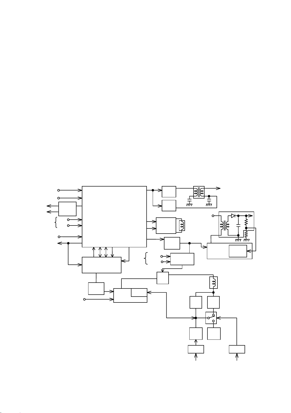
WIRING DIAGRAM
24
Page 25

15P-DSUB
R
G
B
H. SYNC
V. SYNC
SDA
SCL
DDC5V
BUFFER
R
R. G. B . GA I N CONT ROL
G
CL P
B
BLK
C ONT
R
G
B
VIDEO
OUT PUT
BKG
CONTROL
Sync on G Sep.
CONT C-CONT
S-BKG
ACL
BRT BKG S-BKG
CDT
VIDEO PWB
MAIN PWB
V. OUT
ACL
V.OUT
ROTATION
CONTROL
85 V
HEATER
FBT
G1
G2
G3-1
G3-2
EHV
DDC
O SD P W M
SYNC
PRIORITY
CONTROL
VBLK
MUTE
SCL
SDA
V.SYNCB
DSDA
DSCL
H.SYNCB
H.CLAMP
SOGCHK
HBLK
KEY
SW
MICON
HIGH
VOLTAGE
SOGCHK
H.OUT
V.OUT
SDA
SCL
MUTE
ROTATION
LIMIT
HUNLK
H.CENT
H.SIZEC
FHTOV
CS1 - CS6
AC SW
MEMORY
DEGAUSS
6.3V
(HEATER)
SWITCHING
POWER
SUPPLY
SELECTOR
(MPU)
5V
RECTIFIER
H.SYNCB
V.SYNCB
H.IN
V.IN
DSDA
DSCL
MPU
KEY
SW
DG
PS1(STB)
PS2(MODE
O FF)
FUSE
FILTER
H.SYNCA
V.SYNCA
CHOPPER
SDA
SCL
HUNLOCK
B
SWITCHING
POWER
SUPPLY
FILTER
H. SYNCA
V. SYNCA
85V
54V
14V
CLBL
H. V. OSC
FOCUS
V.OUT
BDRV
BRETURN
H.FLB
HDRV
H. DRIVE
CONTROL
DRIVE
HIGH
VOLTAGE
CONTROL
X-RAY
HIGH
VOLTAGE
OUTPUT
HIGH
VOLTAGE
REG IC
EHV
EHV
RETURN
RETURN
+B
(DEF)
H. OUT
DRIVE
+B
H. OUT REG
H. OUT
REG
CONTROL
H.
RETURN
DF OUT
E
HV
REF.
H.CENT
CS6
CS1-5
ACL
H. OUT
G1
REGULATOR
SUB BKG
CS
COIL
+6.3V
HEATER
H. LIN
COIL
H. DY
SW
SM0401
BLOCK DIAGRAM
25
Page 26

P.C.B.A ASSEMBLY
WARNING
1) This product contains components which are critical for X-radiation safety. Read the Service manual
carefully for proper replacement. Maximum 2nd anode voltage use high impedance meter, connect
(-) to chassis, use a high voltage lead from (+) to 2nd anode.
2) Critical Components are marked with the symbol of
in the material list. For continued protection
against X-radiation, replace only with same type and rating components.
3) Critical Components are marked with the symbol of # in the material list. For continued protection
against Low Radiation, replace only with same part number.
4) This symbol warns the personnel that un-insulated voltage within the unit may have sufficient
magnitude to cause electric shock.
Therefore, it should be read carefully in order to avoid any problems.
26
Page 27

THE UPDATED PARTS LIST
FOR THIS MODEL IS
AVAILABLE ON ESTA
Page 28

SM0401
Deflection/Power/MCU Circuit (Main)
39
Page 29

SM0401
Video Circuit
40
Page 30

SM0401
MECHANICAL DISASSEMBLY
42
Page 31

SM0401
ELECTRICAL DISASSEMBLY
43
Page 32

SM0401
DISPLAY UNIT ASSEMBLY
44
Page 33

Attachment A
Page 1 of 5
Procedure to fix the Screen VR on FBT of CM771
1.Preparation
(1) Solder tool with flat head.(Refer to Photo 1 and 2)
2.Operation
(1) Chassis adjustment should be completed.
(2) Attach the head of solder tool softly on the right side of Screen VR knob together with
FBT body for approximately 5 seconds to melt them. (Refer to Photo 3 and 4)
(3) Attach the head of solder tool softly on the left side of Screen VR knob together with
FBT body for approximately 5 seconds to melt them. (Refer to Photo 5 and 6)
(4) Attach the head of solder tool on the top of Screen VR knob for approximately 7
seconds to melt it. (Refer to Photo 7 and 8)
(5) Check Screen VR can not be turned and the G2 voltage is within 600+/-10V.
45
Page 34

Attachment A
Page 2 of 5
Photo 1. Head of solder tool (Side view)
Photo 2. Head of solder tool (Top view)
46
Page 35

Attachment A
Page 3 of 5
Photo 3. Melting right side of VR knob together with FBT body
Photo 4. Melting right side of VR knob together with FBT body (Done)
47
Page 36

Attachment A
Page 4 of 5
Photo 5. Melting left side of VR knob together with FBT body
Photo 6. Melting left side of VR knob together with FBT body (Done)
48
Page 37

Attachment A
Page 5 of 5
Photo 7. Melting top of VR knob
Photo 8. Melting top of VR knob (Done)
49
Page 38

Hitachi, Ltd. Tokyo, Japan
International Sales Division
THE HITACHI ATAGO BUILDING,
No. 15 –12 Nishi Shinbashi, 2 – Chome,
Minato – Ku, Tokyo 105-8430, Japan.
HITACHI EUROPE LTD,
Whitebrook Park
Lower Cookham Road
Maidenhead
Berkshire
SL6 8YA
UNITED KINGDOM
Tel: 01628 643000
Fax: 01628 643400
Email: consumer-service@hitachi-eu.com
HITACHI EUROPE GmbH
Munich Office
Dornacher Strasse 3
D-85622 Feldkirchen bei München
GERMANY
Tel: +49-89-991 80-0
Fax: +49-89-991 80-224
Hotline: +49-180-551 25 51 (12ct/min)
Email: HSE-DUS.service@hitachi-eu.com
HITACHI EUROPE srl
Via Tommaso Gulli N.39, 20147
Milano, Italia
ITALY
Tel: +39 02 487861
Tel: +39 02 38073415 Servizio Clienti
Fax: +39 02 48786381/2
Email: customerservice.italy@hitachi-eu.com
HITACHI EUROPE S.A.S
Lyon Office
B.P. 45, 69671 BRON CEDEX
FRANCE
Tel: 04 72 14 29 70
Fax: 04 72 14 29 99
Email: france.consommateur@hitachi-eu.com
HITACH EUROPE AB
Egebækgård
Egebækvej 98
DK-2850 Nærum
DENMARK
Tel: +45 43 43 6050
Fax: +45 43 60 51
Email: csgnor@hitachi-eu.com
Hitachi Europe Ltd
Bergensesteenweg 421
1600 Sint- Pieters-Leeuw
BELGIUM
Tel: +32 2 363 99 01
Fax: +32 2 363 99 00
Email: sofie.van.bom@hitachi-eu.com
www.hitachidigitalmedia.com
Tel: 03 35022111
HITACHI EUROPE S.A.
364 Kifissias Ave. & 1, Delfon Str.
152 33 Chalandri
Athens
GREECE
Tel: 1-6837200
Fax: 1-6835964
Email: service.hellas@hitachi-eu.com
HITACHI EUROPE S.A.
Gran Via Carlos III, 101- 1
08028 Barcelona
SPAIN
Tel: 93 409 2550
Fax: 93 491 3513
Email: atencion.cliente@hitachi-eu.com
HITACHI Europe AB
Box 77 S-164 94 Kista
SWEDEN
Tel: +46 (0) 8 562 711 00
Fax: +46 (0) 8 562 711 13
Email: csgswe@hitachi-eu.com
HITACHI EUROPE LTD (Norway) AB
STRANDVEIEN 18
1366 Lysaker
NORWAY
Tel: 67 5190 30
Fax: 67 5190 32
Email: csgnor@hitachi-eu.com
HITACHI EUROPE AB
Neopoli / Niemenkatu 73
FIN-15140 Lahti
FINLAND
Tel : +358 3 8858 271
Fax: +358 3 8858 272
Email: csgnor@hitachi-eu.com
HITACHI EUROPE LTD
Na Sychrove 975/8
101 27 Praha 10 – Bohdalec
CZECH REPUBLIC
Tel: +420 267 212 383
Fax: +420 267 212 385
Email: csgnor@hitachi-eu.com
 Loading...