

Page 1
SERVICE MANUAL
MANUEL D'ENTRETIEN
WARTUNGSHANDBUCH
CAUTION:
Before servicing this chassis, it is important that the service technician read the “Safety
Precautions” and “Product Safety Notices” in this service manual.
No. 0410
CM721FET
Data contained within this Service
manual is subject to alteration for
improvement.
ATTENTION:
Avant d’effectuer l’entretien du châassis, le technicien doit lire les «Précautions de sécurité»
et les «Notices de sécurité du produit» présentés dans le présent manuel.
VORSICHT:
Vor Öffnen des Gehäuses hat der Service-Ingenieur die „Sicherheitshinweise“ und „Hinweise
zur Produktsicherheit“ in diesem Wartungshandbuch zu lesen.
Les données fournies dans le présent
manuel d’entretien peuvent faire l’objet
de modifications en vue de perfectionner
le produit.
Die in diesem Wartungshandbuch
enthaltenen Spezifikationen können sich
zwecks Verbesserungen ändern.
SPECIFICATIONS AND PARTS ARE SUBJECT TO CHANGE FOR IMPROVEMENT
MONITOR
December 2001
Page 2

ENGLISH
SAFETY PRECAUTIONS
WARNING: The following precautions must be observed.
ALL PRODUCTS
Before any service is performed on the chassis an
isolation transformer should be inserted between the
power line and the product.
1. When replacing the chassis in the cabinet, ensure
all the protective devices are put back in place.
2. When service is required, observe the original
lead dressing. Extra precaution should be taken to
ensure correct lead dressing in any high voltage
circuitry area.
3. Many electrical and mechanical parts in
HITACHI products have special safety related
characteristics. These characteristics are often not
evident from visual inspection, nor can the
protection afforded by them necessarily be
obtained by using replacement components rated
for higher voltage, wattage, etc. Replacement
parts which have these special safety
characteristics are identified by marking with a
! on the schematics and the replacement parts
list.
The use of a substitute replacement component
that does not have the same safety characteristics
as the HITACHI recommended replacement one,
shown in the parts list, may create electrical
shock, fire, X-radiation, or other hazards.
4. Always replace original spacers and maintain lead
lengths. Furthermore, where a short circuit has
occurred, replace those components that indicate
evidence of overheating.
5. Insulation resistance should not be less than 2M
ohms at 500V DC between the main poles and
any accessible metal parts.
6. No flashover or breakdown should occur during
the dielectric strength test, applying 3kV AC or
4.25kV DC for two seconds between the main
poles and accessible metal parts.
7. Before returning a serviced product to the
customer, the service technician must thoroughly
test the unit to be certain that it is completely safe
to operate without danger of electrical shock. The
service technician must make sure that no
protective device built into the instrument by the
manufacturer has become defective, or
inadvertently damaged during servicing.
CE MARK
1. HITACHI products may contain the CE mark on
the rating plate indicating that the product
contains parts that have been specifically
approved to provide electromagnetic
compatibility to designated levels.
2. When replacing any part in this product, please
use only the correct part itemised in the parts list
to ensure this standard is maintained, and take
care to replace lead dressing to its original state,
as this can have a bearing on the electromagnetic
radiation/immunity.
PICTURE TUBE
1. The line output stage can develop voltages in
excess of 25kV; if the E.H.T. cap is required to be
removed, discharge the anode to chassis via a
high value resistor, prior to its removal from the
picture tube.
2. High voltage should always be kept at the rated
value of the chassis and no higher. Operating at
higher voltages may cause a failure of the picture
tube or high voltage supply, and also, under
certain circumstances could produce X-radiation
levels moderately in excess of design levels. The
high voltage must not, under any circumstances,
exceed 29kV on the chassis (except for projection
Televisions).
3. The primary source of X-radiation in the product
is the picture tube. The picture tube utilised for
the above mentioned function in this chassis is
specially constructed to limit X-radiation. For
continued X-radiation protection, replace tube
with the same type as the original HITACHI
approved type
4. Keep the picture tube away from the body while
handling. Do not install, remove, or handle the
picture tube in any manner unless shatterproof
goggles are worn. People not so equipped should
be kept away while picture tubes are handled
LASERS
If the product contains a laser avoid direct exposure to
the beam when the cover is open or when interlocks are
defeated or have failed.
Page 3

FRANÇAIS
CONSIGNES DE SECURITE
AVERTISSEMENT: vous devez respecter les précautions suivantes
POUR TOUS LES PRODUITS
Avant d’effectuer une intervention d’entretien sur le
châssis, vous devez insérer un transformateur d’isolement
entre la ligne d’alimentation électrique et le produit.
1. Lors de la remontage du châssis dans le coffret,
vérifiez que tous les dispositifs de protection sont
remis en place.
2. Lorsqu’une intervention d’entretien s’avère
nécessaire, respectez l’agencement d’origine des
conducteurs. Vous devez prendre des précautions
supplémentaires pour garantir un agencement correct
des conducteurs dans toutes les zones où des circuits
haute tension sont présents.
3. De nombreux composants électriques et mécaniques
des appareils HITACHI ont des caractéristiques
spéciales de sécurité. Bien souvent, ces
caractéristiques ne sont pas évidentes lors d’un
examen visuel et la protection qu’ils offrent n’est pas
forcément garantie si vous utilisez des composants de
rechange conçus, par exemple, pour une tension plus
élevée, une puissance plus forte. Les pièces de
rechange qui offrent des caractéristiques spéciales de
sécurité sont identifiées par un repérage comportant
le symbole ! sur les schémas et sur la
nomenclature des pièces de rechange.
L’emploi d’un composant de rechange qui ne
respecte pas les mêmes caractéristiques de sécurité
que la pièce de rechange que recommande HITACHI
et qui figure dans la nomenclature risque de
provoquer un choc électrique, un incendie, des rayons
X ou d’autres dangers.
4. Remettez toujours en place les entretoises d’origine
et respectez la longueur des conduites. En outre, à la
suite d’un court-circuit, remplacez les composants
présentant des signes de surchauffe.
5. La résistance d’isolement doit être supérieure ou
égale à 2 méga ohms à 500 V c.c. entre les pôles
principaux et des composants métalliques
accessibles, quels qu’ils soient.
6. Aucun claquage et aucune rupture ne doit se produire
pendant l’essai de résistance diélectrique à la suite de
l’application d’une tension de 3 kV c.a. ou de 4,35
kV c.c. pendant deux secondes entre les pôles
principaux et des composants métalliques
accessibles.
7. Avant de remettre au client un produit qui a fait
l’objet d’un entretien, le technicien qui s’est chargé
de cette intervention doit tester à fond cet ensemble
pour s’assurer qu’il ne présente aucun danger
opérationnel et aucun risque de choc électrique. Ce
technicien doit s’assurer qu’aucun des dispositifs de
protection intégrés à cet instrument par le fabricant
n’est défectueux ou n’a été endommagé de façon
accidentelle lors de l’entretien.
LABEL CE
1. Les produits HITACHI peuvent avoir reçu le label
CE qui figure sur la plaque signalétique pour indiquer
que cet ensemble contient des composants qui ont fait
l’objet d’une homologation spécifique de respect des
normes de compatibilité électromagnétique en
fonction de niveaux bien spécifiés.
2. Lors du remplacement d’un des composants de ce
produit, utilisez uniquement le composant correct
identifié dans la nomenclature afin de maintenir le
respect de cette norme ; en outre, vous devez
également ramener l’agencement des conducteurs à
son état d’origine car cela peut avoir une influence au
niveau des rayonnements électromagnétiques et sur la
protection contre ces rayons.
PICTURE TUBE
1. L’étage de sortie des lignes peut développer des
tensions de plus de 25 kV ; s’il faut retirer le chapeau
de protection contre les tensions extrêmement
élevées, il convient de décharger l’anode contre le
châssis par le biais d’une résistance de forte valeur
avant de déposer ce chapeau du tube image.
2. La haute tension doit toujours se maintenir à la valeur
nominale du châssis et ne pas dépasser cette dernière.
Un fonctionnement à des températures élevées peut
provoquer une défaillance du tube image ou l’entrée
d’une tension élevée. Dans certains cas, cela peut
même provoquer des rayons X d’un niveau
légèrement supérieur aux valeurs de calcul. Cette
haute tension ne doit en aucun cas dépasser 29 kV sur
le châssis (à l’exception des téléviseurs de
projection).
3. La principale source de rayons X de cet appareil est
le tube image. Le tube image employé pour assurer la
fonction susmentionnée dans ce châssis est
spécialement construit pour limiter des rayons X.
Pour maintenir cette protection contre les rayons X, il
faut remplacer le tube d’origine d’un type agréé par
HITACHI par un autre tube de même type.
4. Lors des manipulations, ne tenez jamais le tube
image contre le corps. Pendant toutes les opérations
d’installation, de dépose et de manipulation de ce
tube image, quelle que soit la méthode employée,
vous devez toujours porter des lunettes de sécurité
anti-éclatements. Les personnes qui ne portent pas ce
type de lunettes doivent se tenir à l’écart du tube
image lors de la manipulation de ce dernier.
RAYONS LASER
Si ce produit contient un rayon laser, évitez toute
exposition directe à ce faisceau lors de l’ouverture du
couvercle ou lors de l’élimination des verrouillages de
sécurité ou après défaillance de ces verrouillages.
Page 4

DEUTSCH
SICHERHEITSVORKEHRUNGEN
WARNUNG: Die folgenden Vorkehrungen müssen eingehalten werden.
ALLE PRODUKTE
Bevor die Grundplatte gewartet wird, sollte ein Trenntrafo
zwischen die Netzleitung und das Produkt eingebracht
werden.
1. Wenn die Grundplatte in das Gehäuse zurückgestellt
wird, stellen Sie sicher, dass alle
Schutzvorrichtungen wieder an ihrem Ort sind.
2. Wenn Wartung erforderlich ist, halten Sie die
originale Verdrahtungsart ein. Besondere Vorsicht ist
nötig, um die korrekte Verdrahtungsart in jedem
Hochspannungsstromkreis zu gewährleisten.
3. Viele elektrische und mechanische Teile von
HITACHI Produkten haben besondere
sicherheitsbezogene Eigenschaften. Diese
Eigenschaften fallen oft nicht ins Auge, aber der
durch sie gewährte Schutz kann nicht unbedingt
erreicht werden, wenn man Ersatzteile benutzt, die
für höhere Spannung, Leistung usw. ausgelegt sind.
Ersatzteile, die diese besonderen
Sicherheitsmerkmale haben, sind in den
Prinzipskizzen und Ersatzteillisten an einem ! zu
erkennen.
Der Gebrauch von Ersatzteilen, die nicht dieselben
Sicherheitsmerkmale haben wie die empfohlenen
HITACHI Ersatzteile, wie sie in der Ersatzteilliste
aufgeführt sind, kann zu elektrischem Schlag, Feuer,
Röntgenstrahlung und anderen Gefahren führen.
4. Immer die originalen Abstandsstücke ersetzen und
die Leitungslängen beibehalten. Wo ein Kurzschluss
passiert ist, die Teile ersetzen, bei denen Überhitzung
nachzuweisen ist.
5. Der Isolierwert sollte bei 500 V Gleichstrom
zwischen den Hauptpolen und allen zugänglichen
Metallteilen nicht unter 2M Ohm liegen.
6. Bei der Prüfung auf Durchschlagsfestigkeit sollte
kein Überschlag oder Durchschlag vorkommen,
wenn zwei Sekunden lang 3 kV Wechselstrom oder
4,25 kV Gleichstrom zwischen den Hauptpolen und
allen zugänglichen Metallteilen angelegt wird.
7. Bevor das gewartete Produkt dem Kunden
zurückgegeben wird, muss der Wartungstechniker
das Gerät gründlich prüfen, um sicherzustellen, dass
es betriebssicher ist ohne das Risiko eines
elektrischen Schlages. Der Wartungstechniker muss
sicherstellen, dass keine vom Hersteller im Gerät
eingebaute Schutzvorkehrung schadhaft geworden ist
oder bei der Wartung unabsichtlich beschädigt
wurde.
CE KENNZEICHEN
1. HITACHI Produkte enthalten eventuell das CE
Kennzeichen auf dem Leistungsschild, welches
angibt, dass das Produkt Teile enthält, die eigens
zugelassen sind, um bis zu einem spezifizierten
Niveau elektromagnetische Störfreiheit zu bewirken.
2. Wenn Sie irgendein Teil in diesem Produkt ersetzen,
benutzen Sie bitte nur das korrekte Teil, das in der
Ersatzteilliste aufgeführt ist, um sicherzustellen, dass
dieser Standard eingehalten wird, und geben Sie acht,
die Verdrahtungsart in ihren ursprünglichen Zustand
zurück zu versetzen, weil das einen Einfluss auf die
elektromagnetische Abstrahlung/Störsicherheit haben
kann.
BILDRÖHRE
1. Die Leitungsausgangsstufe kann Spannungen von
mehr als 25 kV entwickeln; wenn die
Höchstspannungskappe entfernt werden muss,
entladen Sie die Anode zum Gehäuse über einen
hochohmigen Widerstand, bevor Sie sie aus der
Bildröhre entfernen.
2. Hochspannung sollte immer auf den festgelegten
Wert des Gehäuses beschränkt bleiben und nicht
mehr. Betrieb bei höherer Spannung kann zum
Versagen der Bildröhre oder zu hoher
Spannungszufuhr führen und kann unter Umständen
auch Röntgenstrahlung hervorbringen, die leicht über
dem Konstruktionsniveau liegt. Die Hochspannung
darf auf keinen Fall 29 kV am Gehäuse überschreiten
(außer bei Projektionsfernsehern).
3. Die Hauptquelle der Röntgenstrahlung im Produkt ist
die Bildröhre. Die Bildröhre, die für die oben
erwähnte Funktion in diesem Gehäuse benutzt wird,
ist eine Spezialkonstruktion zur Begrenzung der
Röntgenstrahlung. Um den Schutz vor der
Röntgenstrahlung zu behalten, ersetzen Sie bitte die
Röhre durch denselben Typ wie den ursprünglichen
von HITACHI zugelassenen.
8. Halten Sie die Bildröhre bei der Handhabung vom
Körper weg. Sie dürfen die Bildröhre nur dann
installieren, entfernen oder handhaben, wenn Sie eine
nicht splitternde Schutzbrille tragen. Personen ohne
derartigen Schutz sollten ferngehalten werden,
solange Bildröhren gehandhabt werden.
LASER
Wenn das Produkt einen Laser enthält, setzen Sie sich
keinesfalls direkt dem Strahl aus, wenn die Abdeckung
geöffnet ist oder wenn die Verriegelung versagt.
Page 5

1. DISPLAY ALIGNMENT .....................................................................................................5
ISPLAY SIZE......................................................................................................................5
A. D
B. P
ICTURE POSITION ..............................................................................................................5
C. L
INEARITY ..........................................................................................................................5
EOMETRY DISTORTION (ALL PRESET MODES)....................................................................5
D. G
E. A
LIGNMENT PROCEDURE.....................................................................................................5
HITE BALANCE ADJUSTMENT (9300°AS MAJOR TEMPERATURE) LOW LIGHT ADJUST........6
F. W
OCUS ADJUSTMENT ...........................................................................................................6
G. F
H. C
ONVERGENCE ADJUSTMENT .............................................................................................6
RESETTING MODES ADJUSTMENT.......................................................................................6
I. P
J. P
OWER ADJUSTMENT ...........................................................................................................7
2. CONTROLS AND CONNECTORS LAYOUT ...............................................................10
A. MAIN PCB .......................................................................................................................10
B. CRT/B ..............................................................................................................................11
C. PIN ASSIGNMENT ..............................................................................................................11
3. CIRCUIT DESCRIPTION................................................................................................12
A. POWER SUPPLY .................................................................................................................12
OWER SUPPLY BLOCK DIAGRAM.....................................................................................12
B. P
C. P
OWER SUPPLY CIRCUIT ...................................................................................................13
D. TDA4855/4858 AUTOSYSNC DEFLECTION CONTROLLER ..................................14
FIGURE (4) (5) .......................................................................................................................14
ORIZONTAL PROCESSOR..................................................................................................16
E. H
F. V
ERTICAL PRE-AMP...........................................................................................................16
ORIZONTAL DRIVE ..........................................................................................................17
G. H
4. TROUBLESHOOTING.....................................................................................................18
A. MONITOR CHECK FLOW CHART........................................................................................19
APPENDIX A: SCHEMATIC DIAGRAMS & PCB ASSEMBLIES ...................................22
APPENDIX B: PARTS LIST.................................................................................................30
APPENDIX C: DISPLAY UNIT ASSEMBLY.....................................................................50
APPENDIX D: CRT & YOKE ASSEMBLY........................................................................53
-4-
Page 6

1. DISPLAY ALIGNMENT
A. Display Size
All preset mode listings in Table 1. shall be within the following limitations:
H. WIDTH: 350 ± 4 mm
V. HEIGHT : 260 ± 4 mm
B. Picture Position
All preset mode listings in Table 1 shall be within the following limitations:
H. PHASESCREEN : SCREEN CENTRE ± 4 mm
V. CENTERSCREEN : SCREEN CENTRE ± 3 mm
C. Linearity
The CONTRAST and BRIGHTNESS control shall be properly adjusted at 15 F-L with Full-intensity reverse
pattern, then change to crosshatch Pattern. The measured values of linearity should be less than 10% when
calculated using all latticrs and should be less than 6% when calculated using adjacent lattices.
The calculation formula was listed below:
H max - H min Vmax-Vmin
x100% or x100%
(H max + H min)/2 (V max + V min)/2
D. Geometry Distortion (all preset modes)
The CONTRAST and BRIGHTNESS control shall be properly adjusted at 15 F-L with full-intensity reverse
pattern, then switch to cross hatch pattern and place unit facing east.
Pincushion should be less than 2.0mm
Barrel should be less than 2.0mm (top & bottom)/ 1.5 (left side & right side)
Trapezoid should be less than 3.5mm Parallelogram should be less than 3.5mm Tilt should be less than 1/2 degree.
E. Alignment Procedure
E-1. Brightness Adjust:
1. Adjust the VR980 so that the +15VS rail is 14.9V±0.1V (The voltage of the C944) in TIMING 1.
2. Check the voltages below :.
C974 : 202 ± 3V
C947 : 76 ± 2V
C946 : 44 ± 1.5V
C940 : 10.4 ± 0.4V
C959 : 12 ± 0.3V
3. Short-Circuit protection function check.
The power source is 230VAC input.
When C944 is shorted, all output voltage should be shut down and unlatch.
When normal condition is recovered, all output voltage should recover automatically.
E-2. Light output adjust
Select Timing 1, preset BRI. And CONT. to max. position.
Adjust G2 to get G2 = 550V ± 10V
Adjust VR803 to get light output = 0.3FL ~ 0.6FL
Select Timing 2, adjust VR405 to get pattern over scan. (H SIZE 100%)
- 5 -
Page 7

F. White Balance Adjustment (9300°as major temperature) Low light
adjust
9300° 6500° 5000°
x = 0.283 ± 10 x = 0.313 ± 15 x = 0.324 ± 15
y = 0.297 ± 10 y = 0.329 ± 15 y = 0.342 ± 15
Y = 0.3 ~ 0.6FL Y = 0.3 ~ 0.6FL Y = 0.3 ~ 0.6FL
1. Select Timing 6, adjust BRI. And CONT. to m ax. disconnect RGB signals, adjus t R/B BAIS to 100 scale (OSD
then slowly adjust G BAIS to 100 scale adjust VR803 to get light output = 0.3 ~ 0.6FL for 9300°, repeat above
steps for 6500° and 5000° R/B GAIN setting to get raster color temperature within specified, finally, adjust
BRI to get raster = 0.06FL.
2. High light adjust
9300° 6500° 5000°
x = 0.283 ± 10 x = 0.313 ± 10 x = 0.324 ± 10
y = 0.297 ± 10 y = 0.329 ± 10 y = 0.342 ± 10
Y =30 FL Y = 30 FL Y =30 FL
Select Timing 4, measure 2 "square, set CONT. to Max, position and SUB-CONT to 127, R/B GAIN to 200, G
GAIN to 200, adjust SUB-CONT to get light output = 35 FL for 9300°, repeat above steps for 6500° and
5000° R/B GAIN setting to get color temperature within specified.
3. Select Timing 3 with full white pattern adjust OSD-ABL (SUB BRIGHTNESS) to get full white light output =
30 ± 2 FL.
-0
+5
-0
-0
+5
+5
-0
+5
G. Focus Adjustment
G-1. Adjust brightness, have the brightness of raster be 0.06FL and contraset be 30FL in timming 6.
G-2. Adjust the G4a and G4b of theFBT, have focus be in the best condition on the 1/4 diagonal of
screen in timing 5.
H. Convergence Adjustment
Input R+B and R+G signals, make sure convergence within specified (if not 4 pole and 6 pole). A zone =
0.3MM., B zone 0.4MM. (X) < 0.4MM, (Y) < 0.4MM.
NOTE : 1. A area = 260mm (circle)
2. B area = 350 x 260 mm
I. Presetting Modes Adjustment
There are 12 preset modes, individual adjust is needed.
1. H-SIZE adjust : adjust control key to get H-SIZE = 350 ± 4mm.
2. H-CENTRE adjust : adjust control key to get centre within ± 4mm
3. V-SIZE adjust : adjust control key to get V-SIZE = 260 ± 3 mm
4. V-CENTRE adjust : adjust control key to get centre within ±2mm
5. Geometric adjust : adjust control key to get minimum distortion.
6. H-linearity check : check and make sure linearity meets spec..
(CROSS HATCH PATTERN 10X8)
2(MAX - MIN)
X100%
MAX + MIN
Any : <10%
Adjacent : <5%
7. V-linearity check : check and make sure linearity meets spec.
- 6 -
Page 8

2 (MAX - MIN)
X100%
MAX + MIN
Any : <10%
Adjacent : <6%
8. Geometric check : check and make sure geometric meets spec.
9. Get into OSD select EE-USER item, press ENTER till OSD disappear then turn off power, disconnect JP1,
turn on power again, make sure all of the alignment parameters has been stored properly, make H-SIZE adjust
range can OVER SCAN and -5%, PHASE adjust range >15mm, V-SIZE adjust range can OVER SCAN and
-6%, V-CENTRE adjust range >20mm and make sure TILT adjust works properly.
J. Power Adjustment
J-1. Adjust the VR980 so that the +15Vs rail is 15.3v±0.1v ( voltage of the C944) in timing 1.
J-2. Check voltages below:
C974 : 202±3v
C947 : 76 ± 2v
C946 : 44 ± 1.5v
C940 : 10.4 ± 1v
J-3. Short-circuit protection function check
1. the power source is 230vac input
2. when C944 is shorted, all output voltage should be shut down and unlatch
3. when normal condition is recovered, all output voltage should recover automatically.
J-4. Side Pincushion, Tilt and Geometry Distortion Adjustment
1. Input timing 1, adjust the display be normal position and size.
2. Adjust front control key to get the best pincushion distortion and tilt.
3. Select P502 and adjust VR402~VR404 to get the best geometry distortion.
J-5. Focus Adjustment
1. Input timing 1, EXT. BRIGHTNESS move to center position. Use EXT.CONTRAST set the
brightness to 25FL.
2. Adjust Focus VR (mounting on FBT), to get best focus.
J-6. Preset Timing Adjustment
1. Input each PRESET MODE timing, and use front control key, adjust the display to the normal
position and size and wait for 5 seconds.
2. Switch to next timing repeat 1 process. Until every PRESET MODE timing has been adjusted.
J-7. Timing And Pattern
Timing mode pattern.mdnm/
1 VESA 80k CROSS HATCH
2 VESA 80K 2" SQUARE
3 VESA 80K FULL WHITE
- 7 -
Page 9
J-8. Power Saving Function Check
The power source is 230Vac input
When the sync signal is removed, the monitor should enter suspend-mode and then off-mode.
When power saving, the power consumption of monitor should be less than: suspend mode 8w off-mode
The monitor recovering time from suspend-mode or off-mode to on-mode should be less than 5 seconds.
TABLE 1
TIMMING MODE PATTERN
1. 64K
2. 37.8K/60HZ
3. 60K Full-white
4. 60K
5. 80K “me”
6. 80K
51 CROSSHATCH
51 CROSSHATCH
5×2″squares
5×2″squares
PRESET MODES TABLE 2
MODE H Pixes
V Lines
d: dot d: display b: back porch p: pulse f: front
1
VGA60 640
480
2
VESA75 640
480
3
VGA70 720
400
4
VESA60 800
600
5
VESA85 800
600
6
VESA60 1024
768
7
VESA75 1024
768
8
VESA85 1024
768
9
VESA60 1280
1024
10
VESA75 1280
1024
11
VESA85
(primary)
12
VESA75 1600
1280
1024
1200
Fd (MHz)
Polar (H/V)
25.175
N/N
31.5
N/N
28.322
N/P
40
P/P
56.25
P/P
65
N/N
78.75
P/P
94.5
P/P
108
P/P
135
P/P
157.5
P/P
202.5
P/P
A: Back Porch (us) B: Display Time (us)
C: Front Porch (us) D: Sync Width (us)
F: Back Porch (ms) G: Display Time (ms)
H: Front Porch (ms) I: Sync Width (ms)
Fh (KHz)
Fv (Hz)
31.469
59.941
37.5
75
31.47
70.09
37.88
60.32
53.674
85.061
48.36
60
60.023
75.029
68.677
84.997
63.981
60.02
79.976
75.025
91.146
85.024
93.75
75
F: Th (us)
F: Tv (ms)
31.778
16.683
26.67
13.33
31.78
14.27
26.4
16.58
18.631
11.756
20.68
16.67
16.66
13.328
14.561
11.765
15.63
16.661
12.504
13.329
10.971
11.761
10.667
13.333
D: Td (us)
D: Td (ms)
25.422
15.253
20.317
12.8
25.422
12.711
20
15.84
14.222
11.179
15.754
15.88
13.003
12.795
10.836
11.183
11.852
16.005
9.481
12.804
8.127
11.235
7.901
12.80
C: Tb (us)
C: Tb (ms)
1.907
1.048
3.81
0.427
1.907
1.112
2.2
0.607
2.702
0.503
2.462
0.6
2.235
0.466
2.201
0.524
2.296
0.594
1.837
0.475
1.422
0.483
1.501
0.491
B: Tp (us)
B: Tp (ms)
3.813
0.064
2.032
0.08
3.813
0.064
3.2
0.106
1.138
0.056
2.092
0.124
1.219
0.05
1.016
0.044
1.037
0.047
1.067
0.038
1.016
0.033
0.948
0.032
A: Tf (us)
A: Tf (ms)
0.636
0.318
0.508
0.026
0.636
0.381
1
0.025
0.569
0.019
0.369
0.063
0.203
0.017
0.508
0.014
0.444
0.016
0.119
0.013
0.406
0.011
0.316
0.011
- 8 -
Page 10
- 9 -
Page 11
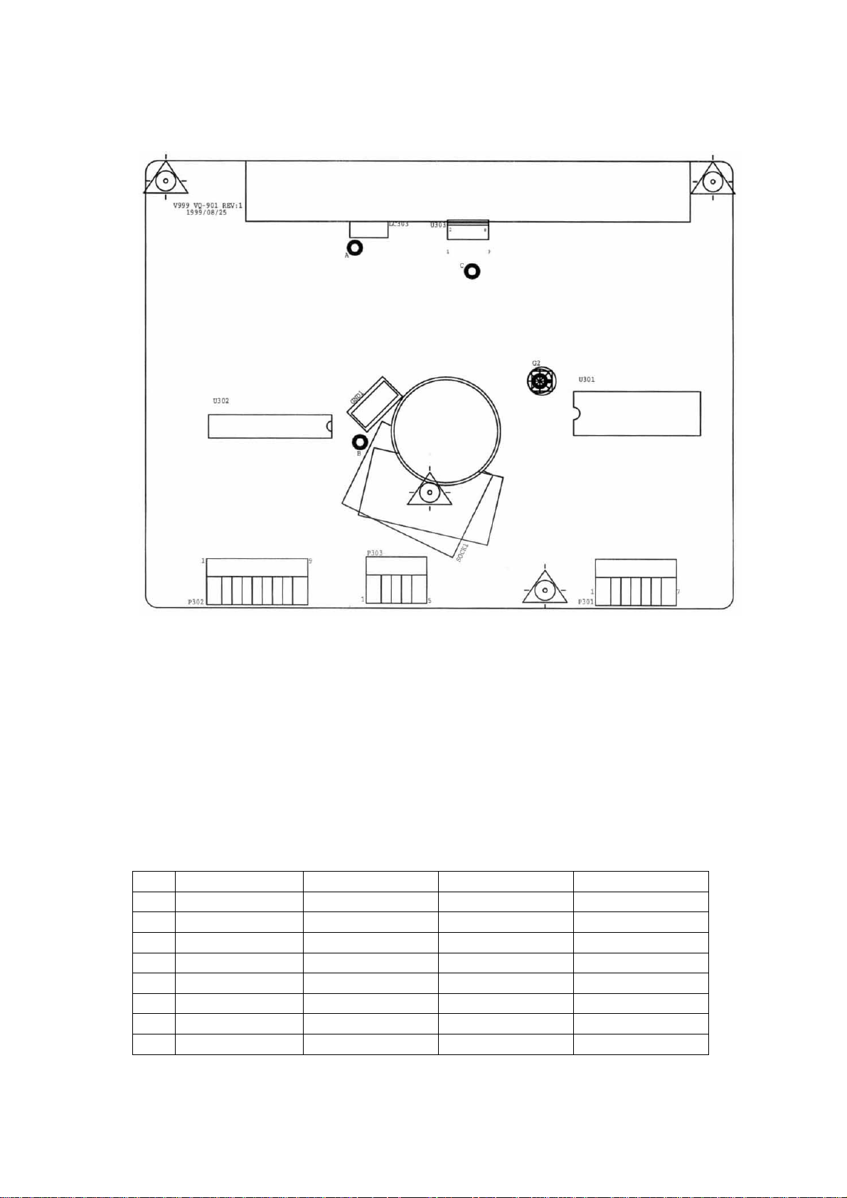
2. CONTROLS AND CONNECTORS LAYOUT
A. Main PCB
- 10 -
Page 12
B. CRT/B
C. Pin Assignment
C-1. Connect Function
VR501 : H-CENTRE VR
P701 : TILT CONN
JP1: PRESET CONN
P902 : DEGAUSSING COIL CONN
P703 : X-RAY TEST PAD
-- P302 P303 P301 P5
1 HFLB Vout DSUB9 DDC-SCL
2 GND EEP-SCL R-IN DDC-SDA
3 G1 EEP-SCL GND GND
4 6.3V H-OUT B-IN V-SYNC
5 5V GND GND H-SYNC
6 76V -- G-IN -7 12V -- GND -8 CONTRAST -- -- --
- 11 -
Page 13

3. CIRCUIT DESCRIPTION
A. Power Supply
The F900 power supply is a universal switching mode power supply. It consists of an off-line
flyback converter and a Boost converter. The output voltage and current rating are +7.5V /
0.81A, +15.3V / 0.84A, +44V /0.2A, +76V / 0.2A, and B+ +202V / 0.4A.
B. Power Suppl y Block Diagram
- 12 -
Page 14

C. Power Supply Circuit
C-1 RECTIFIER AND FILTER CIRCUIT
The 90Vac 260Vac input line voltage is rectified by DB901, and smoothed by C906 via the PFC circuit to
provide DC operating voltage for the circuit.
C-2 FLYBACK AND PWM CIRCUIT
When power is initially applied to the circuit, C909 charg es throu gh R903 an d Q901. Wh en the voltag e across
C909 reaches a level of 16V, U901 is enabled, turning on Q903 and turning off Q901 to complete start-up
action.
During the On-time of Q902, energy is stored in T902. At this time th e polari t y of the output win dings i s su ch
that all output rectifiers are reverse biased and no energy is transferred.
Primary current is sensed by R914 an d compared to a DC level that is determined by volt age f eedback. When
this level is reached, Q902 is turned off and the polarity of all T901A windings reverses, forward biasing the
output rectifiers. All the energy stored is now transferred to the output capacitors. Many cycles of this
store/release action are needed to charge the outputs to their respective voltages.
The main voltage (202V) across R944, R945, R947, C956, R946, VR901 is smoothed by C945 and fed via
the optp-coupler U900 to the primary regulator to the error amplifier (U901 pin1).
C-3 SNUBBER CIRCUIT
Energy stored in the leakage inductance of T902 cause a voltage spike which be added to the normal reset
voltage across T902 when Q902 turn off. The clamp consisting of D905, R904 and C907 limits this voltage
excursion from exceeding the Vds ratin g of Q902. In addition , a tu rn off sn u bber m ade u p of D906, R 90 5 and
C908 keeps power dissipation in Q902 low by delaying the voltage rise until drain cu rrent has decreased f rom
its peak value. This snubber also damps out any ringing which may occur due to parasitic.
C-3 SYNCHRONIZED CIRCUIT
The oscillator frequency is defined by R912, C920. The equation is approximately:
Fosc=1.8/(R912*C920). The external signal that comes from horizontal circuit synchronises the working
frequency of power circuit Via U980 to U906 (PIN 2). For divide frequency in over 50KHz by U906
(74LS221)
C-4 POWER SAVING CIRCUIT
The monitor has ON, Suspend/Standby and OFF states. The monitor enters Suspend/Standby mode if either
V-sync or H-sync signals are removed. When the machine in th e Suspend/Standby state, PS1 s hould be low to
turn off +15Vs. In this state, input power should be less than 15W and LED illuminate yellow. The monitor
enters OFF mode if both H-sync and V-syn c are removed. Wh en in the OFF St ate, PS1 and PS 2 sh ould below
simultaneously to turn off +15Vs and +7.8Vs outputs. In this state, input power should by less than 5W and
LED illuminate amber.
C-5 DEGAUSS CIRCUIT
The DEGU signal which comes from micro-p to control degauss coil act or not.
When DEGU is high, Q946 will be saturated to make RL901 working, AC line provides a degaussing current
to degauss coil.
C-6 OVERLOAD ROTECTION CIRCUIT
The primary curr ent flows through the current sensing resistor R914. The voltage drop on R914 will be
rectified by D921 and keep a dc level in C921 that is dependent on the output power. When this DC level
reach the trigger voltage of Q912, the pin1 of U901 goes low and the power stage is immediately switched
off.
C-7 BROWN-OUT CIRCUIT
When the input voltage down below the setting level (85Vac-70Vac), Q914 will be supplied with a trigger
voltage, pin 1 of U901 goes low and the power stage will be shut down.
- 13 -
Page 15

C-8 PFC CIRCUIT
The PFC CKT is combined with U991A, D901A, T901A..., it is an active type, called” Booster Follower”
circuit.
The feedback points of U991A is not only connected to C906, but also the AC line-in voltage of C901A which
the voltage waveform shape is same as the line-in voltage.
The follower booster circuit can smooth the input current to improve PF value.
D. TDA4855/4858 AUTOSYSNC DEFLECTION CONTROLLER
Figure (4) (5)
- 14 -
Page 16

Pinning
SYMBOL PIN DESCRIPTION
HFLB
1 horizontal flyback input
XRAY 2 X-ray protection input
BOP 3 B+ control OTA output
BSENS 4 B+ control comparator input
BIN 5 B+ control OTA input
BDRV 6 B+ control driver output
HDRV 7 horizontal driver output
GNDP 8 ground (power ground)
Vcc 9 positive supply voltage
FOCUS 10 H- focus parabola output
EWDRV 11 EW parabola output
VOUT2 12 vertical output 2 (ascending sawtooth )
VOUT1 13 vertical output 2 (ascending sawtooth )
VSYNC 14 vertical sync input /output
HSYNC 15 horizontal / composite sync input
CLBL 16 video clamping pulse / V-blanking output
VPOS 17 V- shift input
VAMP 18 V- size input
VSCOR 19 vertical S -correction input
EWTRP 20 Ew trapezium correction input
EWPAR 21 Ew parabola amplitude input
VAGC 22 external capacitor for V-amplitude control
VREF 23 external resistor for vertical oscillator
VCAP 24 external capacitor for vertical oscillator
GNDS 25 ground (signal ground)
HPLL1 26 external filter for PLL 1
HBUF 27 buffered f/v voltage output
HREF 28 reference current for horizontal oscillator
HCAP 29 external capacitor for horizontal oscillator
HPOS 30 H- shift input
HPLL2 31 external filter for PLL 2/soft start
EWWID 32 H-size input
D-1. Sync processor
Pin 15 accepts H or H+V sync.
Pin 14 in H/V separate signal is input-mode, in H/V composite signal is output-mode. This
function is used as mode detector.
- 15 -
Page 17

E. Horizontal Processor
H sync go through TDA4855 internal separation circuit to the first comparator for HOR. Phase ADJ
and then to stage output. A HOR. Drive pulse from pin 7 and input H-sync limit is setting by R431,
R432 and C415.
E-1. Geometric distortion correction
The E-W parabola output from pin 11 is controlled DC CONTROL (pin 20 & 21) and this
parabola go through Q404-Q407 input to pin30 (HOR. Phase ADJ.) for pin-balance ADJ. and
also go through Q408-Q411 for parallel ADJ. And through Q412-Q414 for corner ADJ.
F. Vertical Pre-Amp
VERT. Sync input to VERT. OSC. and generates a saw-tooth at pin 24, the free-run frequency is
setting by R428 and C412 & (fvo=1/10.8 x R428 x C412 & C445), the V-position is controlled by the
D-C (pin 17), and V-size is controlled by D-C (pin 18), and the pin 19 is to ADJ. VERT. linearity.
F-1. VERT output circuit U601 (TDA 8351) see Figure (6)
The saw-tooth is output from U401 pin # 12 & 13. to the pins # 1 and 2 of TDA8351 (vert output
amplifier) and then output from pin # 7 to the vert DY for vert. deflection.
F-2. Horizontal size modulation
To modulation H-size control DC is achieved by applying a parabola to the pins 3 and 5 to
control U402 mono-stable to generate a square wave to drive Q505 thus obtaining a variable
B+ which is input frequency dependent.
31.5KHz T=31.75mS
6.8 to 8.6 mS
HOR.B+=200V x = 43.2 to 54.7V
31.75 mS
95KHZ T=10.526 mS
6.8 to 8.6 mS
HOR.B+=200V x = 130 to165V
10.526 mS
- 16 -
Page 18

G. Horizontal Drive
The drive pulse output from pin 7 of U401 (TDA 4855) through a buffer (Q416/ Q417) and drive stage
(Q503, T501), drives the HOR. Output transistor (Q504).
G-1. CS Circuit
CS control is multiple type the SW1/ SW2/ SW3/ SW5 of U1 to control Q512/ Q520/
Q514/Q515
CS transistor switch Ref. To Fig. Below-
G-2. HORIZONTAL Linear
The D-C HOR. linear control circuit outputs a duty cycle (PWM) through Q545 & Q546 to
the winding of L501 to ADJ. the inductance of linear coil of L501.
G-3. HV circuit
A reference v oltag e is der ived from the bleede r of FBT and in put to U801 (P WM m odulator I C)
to drive Q801.
When Q801 turns on the energ y is stored in t he FBT. When Q801 turns off, the resonate circui t
creates a pulse to the FBT to genera te a HV (*25 KV / 26KV) and G5 voltag e (6.1 ~7.8 KV) a nd
G1 voltage (-180V) and +32V for X-RAY protection and +300V for dynamic focus.
H. Video Amp Circuit
H-1. Video PRE AMP
U301 (M52743) is the Video PRE-AMP. The input signal is 0.7Vp-p, the pre-amp IC U301
amplifies the video signal to be 3-4 Vp-p and controls white balance and contrast.
H-2. Video output AMP
This stage including AMP IC (U303) amplifies the video signal to be around 40Vp-p and
drives the CRT cathode.
H-3. OSD signal
The Mirco-p output DATA and CLK, to the OSD IC U302 (CM46542) and output data on
the VIDEO OUTPUT.
- 17 -
Page 19

4. TROUBLESHOOTING
Start
Check and repair EMI Filter
Check Yes and Q901-Q902
fuse open R932,R963, DB901-DB904
Is Check and repair Q903 U903
Q903 VDS No D982, M907, M911, D912
Waveform normal?
Is 7.5V No Check Q902 D926 C937
In spec U904 U908 VR901
Q909
Correct? Q909
Is B+voltage No Check Q902 Q921 D924 U902A
202V
Ready is
Combine with
Monitor, check operation
frequency
OK
Stop
- 18 -
Page 20

A. Monitor Check Flow Chart
A-1. No raster
-19-
Page 21

A-2. No Picture
-20-
Page 22

A-3. No vertical deflection (raster become a horizontal line)
- 21 -
Page 23

APPENDIX A: SCHEMATIC DIAGRAMS & PCB ASSEMBLIES
- 22 -
Page 24

1234
D
C
B
A
GREEN
V-MODE
AMBER
5V
MUTE
TO U4 12V
TO Q952 C
SW1
POWER ON/OFF
R65
SW2
1.3K
FUN+
1%
SW3
FUN-
SW4
ADJ+
SW5
ADJ-
GND
R80
4.7K
GND
R10
470
8.4V
R72
100
10K
2SC945
1N4148
R33
47K
RN1203
R7
5.6K
1%
R71
1%
JP1
Q1
HZ7A1
D3
Q3
P2
KEY-IN
R4
5.1K
1%
R5
2.7K
LED1
LED2
GND
1
2
3
4
1%
R6
1%3.6K
XXR73
R64
C7
.01U
1M
GND
2
1
D1
1N4148
8.4V
R63
2.7K
D2
1N4148
ZD1
R34
Q2
2SC945
1N4148
R11
1K
1/4W
GND GND
4.7k
+
C70
47U
TO U401 PIN3
GND
GND
R8
10K
1%
33PC5
C42
XX
D406
R1
4.7K
+
10U
16V
GND
V-SIZE
H-PHASE
HSIZE
RESET
33PC6
8MHzY1
KEY-IN
FAT.
M
PS1
PS2
SW1
ZD2
HZ5C1
C9
100U
10V
C4
1
DAC2
2
DAC1
3
DAC0
4
RESET
5
VDD
6
GND
7
OSCO
8
OSCI
9
P15
10
P14
11
P13
12
P12
13
AD1/P11
14
AD0/P10
15
INTE/P16
16
P27
17
P26
18
P25
P24
P23 P22
GND
+
C10
.01U
R38
10K
GND
R37
10K
U1
UM6861
R13
8
7
U2
24C08
2
1
R39
R36
10K
5.6k
VSYNCI
HSYNCI
DAC3
DAC4
DAC5
DAC6
DAC7
HSYNCO
VSYNCO
DAC13
DAC12
DAC11
DAC10
DAC9
DAC8
DDC-SCL
DDC-SDA
100
R14
100
6
54
3
P20
P21
H
L
H
H
L
U4
+
58K-66K
L
H
H
H
LL
76K-89K66K-76K
L
H
H
H
H
H
HH
H
D5
XX
I
7812
G
GND
12V
O
+
C14
220U
16V
R40
10K
+
C8
220U
10V
GND GNDGND
R35
5.6k
C3
.01U
10KX8
5V
RA1
7805
O
+
C2
2200U
10V
GND GND
1/4W
R43
D4
XX
U3
G
10K
I
1/4W
10K
R45
1/4WR70
2.2K
1/4WR47
10K
7.5V
C1
.01U
1/4WR48
10K
R49
4.7K
R50
4.7K
SW1
SW2
SW3
SW4
SW5
31K-33K
L
L
L
R178.2K
HL
L
36.1K-40K
L
H
33.1K-36K
LL
HL
H
HH
16VS
52.1K-58K40.1K-52K
L
L
H
H
L
C13
47U
25V
R68 10K
5V
40
39
38
37
36
35
VSYNC
HSYNC
VCENT
PIN.
TRAP.
TILT.
D14
1N4148
D16
1N4148
GND
34
33
32
31
30
29
28
27
26
25
(POSITIVE)
H-OUT
(NEGATIVE)
V-OUT
CORNER.
PARA.
BALA.
5V
BRI. BRI
D10
1N4148
5V
D13
1N4148
24
23
2219
2120
C40
100P
5V
7.5VS
SW4
SW5
SW2
100P
GND
C41
D8
1N4148
D6
1N4148
L30
BEAD
R100
3.3
2W
GND GND
L31
BEAD
5V5V
V350
G1
GND
H-BLK
6.3V
12V
ABL
82V
C31
.01U
100V
D11
1N4148
D9
1N4148
D7
1N4148
GND
GND
GND
C45
.1U
GND
C32
.01U
GND
P1
1
2
3
4
5
6
7
8
9
D12
1N4148
V-OUT
CLAMP
C36
100P
GND
EEP-SDA
EEP-SCL
GND
GND
C39
100P
P3
1
2
3
4
5
L8
5V
D15
1N4148
D17
1N4148
GND
C11
2200P
GND
R161001/4W
100
R15
1/4W
5V
BEAD
DDC-SCL
BEADL7
DDC-SDA
GND
BEADL5
V-SYNC
H-SYNC
BEADL6
C37
220P
GND GND
R69 10K
DEG.DEG.
DDC-SCL
DDC-SDA
R62
1K
1/4W
P5
1
2
3
4
5
C38
220P
R20 1001/4W
R21 1001/4W
R22 10K1/4W
R23 10K1/4W
R24 10K1/4W
R25 1001/4W
R26 10K1/4W
1/4W10KR30
R28 10K 1/4W
R29 10K 1/4W
10K 1/4WR27
R31 10K 1/4W
Q5
2SC945
+
C25 4.7U
4.7UC29+4.7UC30
+
4.7U
C15
+
4.7U
+
C16
4.7U
4.7U
+
C17
R59
4.7K
1/4W
4.7UC21+4.7UC20+4.7U
+
+
C18
GND
C19
4.7U
+
C23
4.7UC24
+
C27
470P
R60
R61
10K
GND
10K
Q4
2SC945
R58
10K
GND
R57
10K
C26
1000P
HITACHI (EUROPE) LTD
Title
SCHEMATIC, DEF & POWER VA-916/
SWITCH BOARD VR-916
Sheet 1 of 3
89K-
H
H
H
L
H
H-SIZE
H-PHASE
V-SIZE
V-CENT
PIN
TRAP
TILT
H-MORIEH-MORIE
CONNER
PARALLEL
BALANCE
V-MORIEV-MORIE
H-SYNC
V-SYNC
Page 25

1234
D
C
B
A
H-SIZE
12V
B-DRIVE
H-DRIVE
15VS
H-MORIE
V-MORIE
U601-P9
HFLB
V-OUT
H-OUT
Q814-E
X-RAY
X-RAY
CLAMP
V-CENT
V-SIZE
V350
V-MODE
PIN
TRAP
12V
BLANCE
PARALLEL
CORNER
H-PHASE
1
R456
6.8K
R402
P730
R730
5.11K
R424
470K
1/4W
GND
2SC945
Q404
3
2
R455
4.7k
GND
1
1%
47K
Q401
RN1203
R405
+
C446
470U
16V
GND
4
100
1/4W
2
R731
4.3K
1/4W
1%
R459
22K
1/4W
2SC945
Q405
R447
430k
1/4W
5
R441
150K
GND
R454
56K
1/4W
7
6
GND
R476
1K
R477
1K
R416 100
R732
7.32K
1%
U402
AN5767K
9
8
R457
5V
R478
10K
D420
1N4148
ZD730
HZ12C1
GND
GND
2SC945
Q406
10
220K
GND
GND
C730
10U
GND
R426
47K
1/4W
11
R450
220K
Q432
2SC945
Q428
GND
13
12
GND
R463
22K
GND
C404
470P
GND
+
R733
1K
GNDGND
R423 39K 1/4W
12V
C455
XX
XX
R427
56K
1/4W
2SC945
2SC945
Q407
R466
680K
1/4W
R462
33K
GND
Q408
C406
25V NP
Q732
R401
240K
1/4W
R403
47K
1/4W
R410
33K
10U
R411
R734
2.2K
Q731
2SA733
2SC945
GND
R400
51K
2SC945
Q409
R408
150K
1/4W
10K
1/4W
C433
470P
R489
1/4W
2.2
(FUSE)
Q417
2SC945
D405
1N4148
Q416
2SA733
C424
.1U
MEF
GND
R601
100
1/4W
C444
100P
GND
16 15 14 13 12 11 10 9 8 7 6 5 4 3 2
R603
GND
R417
100 1/4W
100PC443
10
1/4W
R418
1.2K
1/4W
+
C408
470U
16V
U401
TDA4858
(FUSE)
MEF.1UC422
R428
22K
1%
.1U
C412
MEF
C413
GND
.0022U
PPN
R434
150K 1/4W
R440
270K
2SC945
Q410
2SC945
Q411
R444
330K
2SC945
Q412
1/4W
GND
D404
1N4148
ZD404
HZ5C1
R419
3.3K
GND
R429
8.2K
R432
750
1%
C414
.22U
MEF
2SC945
Q413
R465
120K
1/4W
R404
6.2K
1/4W
GND
R431
1%
C415
.01U
PPN
R464
7.15K
1/4W
1%
1%1.24K
2SC945
Q414
ZD491
HZ12C1
C437
100U
16V
2SA733
Q424
C428
1500P
MEF
2%
C410
.01U
R420
R437 620K
C416
2SC945
R409
270K
GND
+
GND
MEF
32313029282726252423222120191817
27K
MEF.01U
R407
13K
1/4W
Q438
GND
R449
47 1/4W
(FUSE)
R451
2.2K
1/4W
GND
GND
MEF.01UC438
MEF.012U
R406
C417
+
GND
R430
10K
C440
220P
2.2M
C491
470U
16V
2SC945
Q422
2SA733
R491
1/4W
(FUSE)
Q420
220
D491
FR104
D494
1N4148
+
C427
100U
16V
GND
D430
1N4148
D431
1N4148
GND
R487
R422
1.5K
1/4W
(FUSE)
C601
R436 56K
100
R620
XX
R623
5.36K
R621
100
1%
R607
43V
ZD442
HZ12C1
R482
C434
.01U
MEF
4.7K
R481
10K
R442
4.7K
NO NOTES ? W RESISTOR IS 1/8W
N0 NOTES ? V CAPACITOR IS 50V
XX
2W
1
15V
R494
100
1/4W
C512
.1U
250V
MEF
+
C603
2200U
25V
105C
GND
R443
2.2K
1/4W
Q442
2SD667
GND
FORM U401
PIN 26
U601
TDA8351
R604 1W1
C435
R468
10K
C604
100U
63V
R605
33K
MEF.1U
250V
+
VR405
R736
10K
C613
220P
R606
1/4W
20K
10K
2
3
R412
1/4W
R452
100K
1/4W
R614
GND
-
+
R461
36K
1/4W
10K
47
1/2W
R611
180
1/2W
1
C432
.1U
Q430
2SC945
(FUSE)
G1
V-OUT
Title
1%
+
C411
22U
25V
GND
R453
10K
C448
.1U
U403
LM358
6
5
22.1K
MEF
-
+
R413
1%
D421
1N4148
R473
1/4W
2.2K
(FUSE)
C470
150p
7
R469
200K
1/4W
Q431
2SC2001
R474
1K
R471
18.2K
R480
10K 1/4W
R472
9.09K
GND
1%
1/4W
GND GND
987654321
42V
D612
1N4148
R613
L611
100uH
R609
2.7K
1/4W
1
2
10
1/4W
+
GND
C605
1U
D611
.1UC602
R610
12K
+
GND
3
4
P501
HITACHI (EUROPE) LTD
SCHEMATIC, DEF & POWER VA-916/
SWITCH BOARD VR-916
Sheet 2 of 3
FBP
MUTE
5V
R475
1K
GNDGND
1N4148
GND
15VS
V-DF
C606
2.2U
H-BLK
C471
.1U
MEF
HFLB
FOR 456A49-01
446A49-01
Page 26

43V
H-DRIVE
MUTE
RN1203
SW5
15VS
SW4
SW1
SW2
SW3
210V
X-RAY
FBP
TILT
7.5VS
ABL
Q548
R705
10K
GND
R580
2.2K
1/4W
C563
10U
C812
.01U
R702
2.2K
1/4W
MEF
R579
2.2K
1/4W
GND
R571
2.2K
1/4W
Q506
RN1203
GND
R817
Q703
2SC945
GND
R818
3.3K
1/4W
R701
2.2K
1/4W
C703
10U
25V
Q547
RN1203
GND
GND
R537
100
D508
1N4148
R520
2.2K
1/4W
Q507
RN1203
D509
1N4148
Q516
BF421
1/4W47K
(FUSE)1/2W
GND
Q701
2SC945
+
GND
Q702
2SA733
C501
47U
63V
105C
R578
1K
"A"
D808
1N4148
GND
+
GND
R538
1
2W
+
C524
4.7U
250V
Q803
2SC945
R703
2.2
1/4W
(FUSE)
GND
R521
2.2K
1/4W
Q508
RN1203
GND
R539
100
1/2W
(FUSE)
R816
330
1/4W
C701
25V
GND
P701
1
L90
TO ROTATE COIL
R506
220
1/4W
R550
22K
R549
2.2K
1/4W
Q510
RN1203
GND
R536
2.2K
1/4W
Q509
RN1203
GND
R502
.2
1W
FUSE
+
10U
2
L89
BEAD
R503
R507
1/2W
R551
GND
L506
100UH
100U
R814
10
1/4W
(FUSE)
2W220
Q501
2SD669
220
Q502
2SD669
330
1/4W
C803
250V
105C
GND
C822
100U
16V
R522
1/2W
C513
1200P
1KV
+
GND
C829
22U
C809
47U
25V
+
220
+
GND
R504
100
5W
+
GND
R542
R510
100
1/4W
C541
.1U
400V
MPA
D803
31DF6
GND
C823
100P
5
U801
3843
76
5W120
C502
.22U
MEF
L501
4503
C511
.12U
250V
MPA
Q819
RN1203
D810
1N4148
GND
7.5VS
2SB647AC
R821
47K
1/4W
348
1
2
GND
R508
560
1W
R509
10K
1/4W
Q952-C
R815
470
1/4W
Q545
GND
C539
.1U
R806
220K
C531
3300P
PPN
R546
39
2W
C810
2200P
GND
R541
100
1N4148D541
D804
BYV36C
GND
DGQ503
2SK941
S
GND
Q546
2SA733
C516
.01U
GND
C801
3300P
1.6KV
R812
12K
R820
1K
1/2W
PPS
R804
10K
1/4W
GND
T501
R545
4.7K
FR104
G
R544
10K
1N4148
GND
U403-P7
D542
D
IRFS640A
S
GND
R811
150
1/4W
D823
C515
.1U
400V
MPA
Q517
D802
UF5408G
HS801
G
R823
68
R803
10K
R826
680K
D507
BYD73A
R530
100
C532
.01U
D
S
GND
D526
FR104
IRFS640A
D801
BYM36E
Q801
2SK1341
R801
0.2
2W
(R)
GND
(R)2.2 2WR512
(R)2.2 2WR514
Q514
G
R531
10K
C834
.01U
GND
2
GND
R513
22
1/2W
D
S
1
+
C846
2.2U
2SC945
C835
.1U
MEF
250V
Q504
2SC5440
HS501
C520
.27U
400V
MPA
D532
1N4148
R532
100
C534
.01U
T801
Q805
GND
D527
FR104
R834
10K
G
R533
10K
C821
XX
R511
D502
5TUZ47C
GND
C508
.0024U
1.6KV
PPS
D519
FR104
C521
.47U
400V
MPP
100R528
IRFS640A
Q515
D
S
+
GND
1
2W
D528
C529
.01U
+
C820
GND
VR802
C542
2200P
1KV
GND
G
1N4148
GND
R827
470
1/2W
14
12
7
44
5
8
9
10
33U
30K
+
C510
GND
1.2U
250V
C519
D
S
GND
R529
GND
R825
82K
1/4W
GND
L504
BEAD
C505
.0024U
1.6KV
PPS
GND
47U
250V
MPP
Q512
IRFS640A
10K
"A"
C506 2KV180P
C530
220P
1KV
Q505
G
B-DRIVE
C523
.047U
400V
PPN
D547
1N4148
D548
1N4148
D549
1N4148
D550
GND
C507
4700P
500V
GND
SW1
SW2
SW3
SW4
R570
JW
R540
4.7K
1/2W
R802
1/4W
P803
R574
4.7K
Q524
RN1203
R517
10K 1/4W
D505
1SS82
C533
.01U
250V
PPN
G
R560
100
P501
YOKE-H
D
2SK941
S
GND
5V
R564
4.7K
1
2
3
4
R535
4.7
Q526
2W
IRF9634
SD
R565
100
XX
GND
+
C817
D814
1N4148
50V22U
R807
47
2W
MOF
D805
HER103
C806 1KV330P
R841
XX
R805
56
1/2W
MOF
D807
UF4006
C807
220P
1KV
SG801
GND
D806
UF4006
R852
150
1W
NO NOTES ? W RESISTOR IS 1/8W
N0 NOTES ? V CAPACITOR IS 50V
10
L509
BEAD
GND
C551
.01U
250V
PPN
GND
SYNC
T506
2810
R575
GND
+
C818
2.2U
400V
+
C819
22U
250V
R862
1/4W
L508
BEAD
D506
BYV26C
GND
C826
2200P
1KV
D
G
S
GND
R576
100
Q525
RN1203
D813
UF4006
FBP
Q519
100
2.2
(FUSE)
GND
2SK941
R577
4.7K
GND
T802
L503
8mH
12x16
Q812
2SC2271
15VS
Q813
2SC945
R833
33K
1/4W
R850
620K
1W
R824
220K
1/2W
D521
FR10-04
R515
HER102
2.2
1/4W
(FUSE)
R516
2.2
1/4W
(FUSE)
R861
240K
1/2W
D809
1N4148
R844
6.8K
R846
300K
R847
330
GND GND
R848
9.1K
1/4W
R849
10K
GND
GND
+
C833
47U
25V
R835
4.7K
2SA733
R836
22K
Title
D503
+
+
GND
16V
16V
C827
2.2U
+
+
VR501
R837
470
5K
C540
R501
1K
XX
ZD801
+
C555
XX
D504
HER102
C554
XX
R860
470K
1/2W
R845
27K
R843
22K
Q814
C562
220U
C561
220U
C828
10U
25V
HZ6B2
Q811
VR803
10K
Q810
BF421
RN1206
GND
R838
180K
R839
C825
150K
.1U
GND
GND
HITACHI (EUROPE) LTD
SCHEMATIC, DEF & POWER VA-916/
SWITCH BOARD VR-916
Sheet 3 of 3
Q522
2SD667
Q521
2SB647
R561
10
1W
L502
880uH
R566
33
2W
+
C522
2.2U
250V
GND
V-DF
HV
X-RAY
15VS
MUTE
BRI
G1
FOR 456A49-01
446A49-01
Page 27

D
C
B
A
L901
L902
100UH
F901
T3.15A
250V
102Y2
LN
1
P901
SOCKET
ZD990
HZ5C1
1
0.47X2
C93A
2
C991
22U
25V
GND5
R989
240
1/4W
R998
1/4W
C902
0.47X
R901
820K
1/2W
MF
C901
3
C977
104Z
C995
102
750
100UH
C931
102Y2
+
R988
3K
GND5
C903
332Y
C904
332Y
4
22mH
32
L904
R996
12.7K
MF
C992
222G
PPN
GND5
GND5
U980
6
5
43
4N35
RT901
15SP008
C983
472Y
74LS221
R995
1.5K
D991
4148
ZD991
HZ5C1
GND5
1
2
GND1
RL901
OMI-SS-212DM
PR901
1
P902
DEGUESS
R990
1W330
Q992
A733
R993
3K
R994
4.7K
1216 15 14 13 11 10 9
C993
391K
R999
4.7K
C982
222
R987
1K
1/2W
DB901
GBU4J
95W
3
2
Q946
C945
U906
87654321
GND5
C990
22U
25V
R979
47
1/4W
D980
FR104
GND5
+-
GND1
+
SYNC
R950
1/2W
D950
4148
Q990
A952L
R991
4.7K
D930
4148
R992
4.7K
1/4W
Q991
C945
C901A
0.68U
630V
MPP
0.75
91
R951
10K
1/4W
+
C996
47U
25V
R976
620K
1WS
MOF
R977
620K
1WS
MOF
R926
91K
R901A
R902A
3W(R)0.75
3W(R)
DG100015000
GND5
16V
GND5
T901A
FS14KM-10
DEGU
A733
C932
221Y1
Q901A
R904A
R905A
1/4W
R912A
15K
R975
1K
Q914
+
C969
4.7U
50V
10K
15K
C913
2.2U
GND5
D909
4148
R931
100K
R913
100K
GND5
ZD902
GND5
C903A
102K
C904A
684J
C906A
221J
NPO
+
R930
1/4W22
*
L907
jumper
GND5
GND5
GND5
GND5
D911
4148
C917
104Z
GND5
R957
22K
C930
100U
10V
R908A
47K
R913A
15K
BT169
C933
1KV
101
D901A
ER306
R906A
1M
1/2W
R907A
1/4W
1M
R903A
L906
BEAD
1/4W10
81
2
7
U991A
MC33260
36
54
G
KA
Q912
ZD901
HZ18-1
D912
*
C922
471K
+
MF
MF
D903A
4148
R911A
1/2W
270
1/4W
GND5
R922
22K
ZD903
HZ5C1
R912
22K
GND5
ZD90A
HZ15-2
+
C902A
100U
25V
+
103
R982
+
C906
100U
450VA
GND5
1/4W
R921
C923
2.2U
50V
C920
MEF
R916
47
GND5
C935
500V
1W(R)0.2F
GND5
+
C924
47U
16V
R909
47
1K
+
C911
1OOU
25VA
GND5
+
C909
100U
25V
GND5
U9013842
332
R927
1M
1/2W
R928
1M
1/2W
D916
4148
C921
220U
GND5
GND5
GND5
GND5
MF
MF
D913
4148
Q903
C945
D921
+
4148
10V
C910
104Z
R943
0.2F
1W(R)
Q901
HTL145
2SK2761
HQ902
GND5
D908
FR104
1367
2548
R903
82K
3W
Q902
G
R917
10K
1/4W
R920
240
1/4W
R914
0.3
3W(R)
D915
FR104
R908
10F
1/4W
C914
103
R911
3K
R904
C962
103
500V
GND5
D
S
33K
1W
L903
BEAD
GND5
R971
1K
1/4W
GND5
D905
FR107
C925
103
500V
GND5
D906
C970
471K
5
C907
103
500V
4
3
1
C908
331
1KV
Y5P
R905
47K
2W
FR107
7
8
C905
472Y
C980
472Y
GND5
T902
DG100012800
12
11
10
13
16
GND1
17
GND1
18
15;14
C900
472Y
C981
472Y
C998
*
4
U900
3
LTV-817MB
101
1KV
C952
331
1KV
D944
ER306
(R)
R985
0.2F
1W
(R)
R973
0.2F
1W
(R)
R972
0.47F
1W
GND1
1
2
C950
D945
ER306
(R)
R981
10
1W
D943
UF5406G
(R)
C963
331
1KV
C954
331
1KV
C955
331
1KV
D923
ER202
U904
TL431
C971
331
1KV
D972
ER306
(R)
R953
10
1W
D942
ER302
R954
10
1/4W
D941
ER202
R955
10
1/4W
R910
3K
0.22U
K
A
GND1
C961
D946
ER306
(R)
R980
10
1W
R941
47
C945
MEF
R
+
C946
220U
GND1
1000U
GND1
R940
R942
1/4W
101
1KV
63V
L944
22U
+
C943
25V
1K
R944
51K
1/2W
R945
51K
1/2W
1KF
L905
22U
16V
GND1
GND1
R946
1KF
1/4W
VR901
500
C973
103
500V
+
C947
100U
GND1
100V
+
C944
1000U
25V
R986
jumper
C941
+
1000U
16V
C964
100U
25V
R947
470F
1/4W
C956
224J
250V
MEF
+
C949
100U
250V
GND1
D951
4148
R963
470
GND1
C953
+
220U
63V
D956
D952
4148
+
R964
4.7K
GND1
R960
180K
1W
GND1GND1
*
B772QQ951
C975
100U
25V
R966
+
C940
470U
16V
GND1
1/2W1K
D957
Q941
B772Q
Title
1234
L947
22U
L945
22U
R984
jumper
+
*
R965
470
1/2W
+
C965
470U
GND1
AMBER
16V
+
C974
47U
250V
GND1
GND1
+
C948
47U
100V
GND1
*
D954
U903
GND1
L941
22U
Q942
C945
Q952
C945
25V100U
7812
GND1
R967
10K
1/4W
jumper
R983
R968
10K
GND1
D959
4148
+
C942
+
C957
47U
16VA
GND1
GND1
R961
620
1/4W
LA54B
Q960
RN1206
YELLOW
GND1
HITACHI (EUROPE) LTD.
SCHEMATIC, POWER, VA-916
C987
103M
500V
+
C959
47U
16V
GND1
R962
1/4W
D923
GREEN
GND1
620
C997
103M
500V
GND1
D955
4148
GND1
Q961
RN1206
202V
76V
44V
16VS
12V
C960
104Z
PS1
7.5VS
PS2
7.5V
FOR HEATER
10.5V
GREEN
NO NOTES ? W RESISTOR IS 1/8W
N0 NOTES ? V CAPACITOR IS 50V
FOR X62A49-01
X61A49-01
Sheet 1 of 1
Page 28

Page 29

Page 30

Page 31

THE UPDATED PARTS LIST
FOR THIS MODEL IS
AVAILABLE ON ESTA
Page 32

APPENDIX C: DISPLAY UNIT ASSEMBLY
- 50 -
Page 33

Page 34

001 FUNCTION KNOB V99921-1 ABS 94HB WG017
001 FUNCTION KNOB V99921-1 ABS 94HB MCG18
002 PCB HOLDER(L) M98021 WG017 ABS
002 PCB HOLDER(L) M98021 WG017 ABS+PC
003 PCB HOLDER(R) M98022 WG017 ABS
003 PCB HOLDER(R) M98022 WG017 ABS+PC
004 RUBBER WASHER M98042 t=5.5-1.6
005 RUBBER PAD M9904F
006 RUBBER PAD(HEATSINK) M9904G
007 COPPER PAPER CBEZEL H9931-1
008 LOCKING CABLE TIE 142MM
009 CUSHION 2 H76748
010 RUBBER WASHER F56146 (T=4.0MM SHORE:50)
011 SCREW M4X0.7+8CF-MC(EX.LOCK WASHER)
012 TAPPING SCREW TPB 4+20N-MC
013 SCREW TPP-3+10C-MC
016 POWER LED LENS V99941
017 LOCKING CABLE TIE W2.5XL203 WHITE (YJ-203S)
018 COPPER PAPER (CRT) H99944
020 SCREW TPB-5+24P-MC
025 SCREW TPP-3+6C-MC
M01 SCREW M4X0.7+8C-MC
M02 SCREW M4X0.7+8P-MC (ADD WASHER)
M03 SCREW TPB-3+8 P-UC
MB1 SCREW TPB-3+8C-MC
MB2 SCREW TPB-3+8C-MC
MB3 SCREW TPB-3+8C-MC
MP01 SCREW TPB-4+8C-MC
MP02 SCREW TPB-4+8C-MC
MXX SCREW M4X0.7+8P-MC (ADD WASHER)
Monitor Assembly
Page 35

APPENDIX D: CRT & YOKE ASSEMBLY
CRT&YOKE Assembly
001 CRT & YOKE M46QCK761X123 SAM AC500025600
002 H-CON SET H999 CRT-GND AROUND W5.6 DC020133320
- 53 -
Page 36

Page 37

Hitachi, Ltd. Tokyo, Japan
International Sales Division
THE HITACHI ATAGO BUILDING,
No. 15 –12 Nishi Shinbashi, 2 – Chome,
Minato – Ku, Tokyo 105-8430, Japan.
HITACHI EUROPE LTD,
Whitebrook Park
Lower Cookham Road
Maidenhead
Berkshire
SL6 8YA
UNITED KINGDOM
Tel: 01628 643000
Fax: 01628 643400
Email: consumer-service@hitachi-eu.com
HITACHI EUROPE GmbH
Munich Office
Dornacher Strasse 3
D-85622 Feldkirchen bei München
GERMANY
Tel: +49-89-991 80-0
Fax: +49-89-991 80-224
Hotline: +49-180-551 25 51 (12ct/min)
Email: HSE-DUS.service@hitachi-eu.com
HITACHI EUROPE srl
Via Tommaso Gulli N.39, 20147
Milano, Italia
ITALY
Tel: +39 02 487861
Tel: +39 02 38073415 Servizio Clienti
Fax: +39 02 48786381/2
Email: customerservice.italy@hitachi-eu.com
HITACHI EUROPE S.A.S
Lyon Office
B.P. 45, 69671 BRON CEDEX
FRANCE
Tel: 04 72 14 29 70
Fax: 04 72 14 29 99
Email: france.consommateur@hitachi-eu.com
HITACH EUROPE AB
Egebækgård
Egebækvej 98
DK-2850 Nærum
DENMARK
Tel: +45 43 43 6050
Fax: +45 43 60 51
Email: csgnor@hitachi-eu.com
Hitachi Europe Ltd
Bergensesteenweg 421
1600 Sint- Pieters-Leeuw
BELGIUM
Tel: +32 2 363 99 01
Fax: +32 2 363 99 00
Email: sofie.van.bom@hitachi-eu.com
www.hitachidigitalmedia.com
Tel: 03 35022111
HITACHI EUROPE S.A.
364 Kifissias Ave. & 1, Delfon Str.
152 33 Chalandri
Athens
GREECE
Tel: 1-6837200
Fax: 1-6835964
Email: service.hellas@hitachi-eu.com
HITACHI EUROPE S.A.
Gran Via Carlos III, 101- 1
08028 Barcelona
SPAIN
Tel: 93 409 2550
Fax: 93 491 3513
Email: atencion.cliente@hitachi-eu.com
HITACHI Europe AB
Box 77 S-164 94 Kista
SWEDEN
Tel: +46 (0) 8 562 711 00
Fax: +46 (0) 8 562 711 13
Email: csgswe@hitachi-eu.com
HITACHI EUROPE LTD (Norway) AB
STRANDVEIEN 18
1366 Lysaker
NORWAY
Tel: 67 5190 30
Fax: 67 5190 32
Email: csgnor@hitachi-eu.com
HITACHI EUROPE AB
Neopoli / Niemenkatu 73
FIN-15140 Lahti
FINLAND
Tel : +358 3 8858 271
Fax: +358 3 8858 272
Email: csgnor@hitachi-eu.com
HITACHI EUROPE LTD
Na Sychrove 975/8
101 27 Praha 10 – Bohdalec
CZECH REPUBLIC
Tel: +420 267 212 383
Fax: +420 267 212 385
Email: csgnor@hitachi-eu.com
 Loading...