

Page 1
SERVICE MANUAL
MANUEL D'ENTRETIEN
WARTUNGSHANDBUCH
CAUTION:
Before servicing this chassis, it is important that the service technician read the “Safety
Precautions” and “Product Safety Notices” in this service manual.
No. 0502
CM615ET
CM615ET302
CM615ET303
CM615ET321
Data contained within this Service
manual is subject to alteration for
improvement.
ATTENTION:
Avant d’effectuer l’entretien du châassis, le technicien doit lire les «Précautions de sécurité»
et les «Notices de sécurité du produit» présentés dans le présent manuel.
VORSICHT:
Vor Öffnen des Gehäuses hat der Service-Ingenieur die „Sicherheitshinweise“ und „Hinweise
zur Produktsicherheit“ in diesem Wartungshandbuch zu lesen.
Les données fournies dans le présent
manuel d’entretien peuvent faire l’objet
de modifications en vue de perfectionner
le produit.
Die in diesem Wartungshandbuch
enthaltenen Spezifikationen können sich
zwecks Verbesserungen ändern.
SPECIFICATIONS AND PARTS ARE SUBJECT TO CHANGE FOR IMPROVEMENT
OCTOBER 2000
Page 2

1111. DISPLAY ALIGNMENT
A. Times & Display Size
For all presetting mode listing in section 2.4 shall be within the limitation:
H. WIDTH 306 ± 4 mm
V. HEIGHT 230 ± 4 mm
The external control range of the data area, shall be as follows;
Max. horizontal size : overscan the screen
Min. horizontal size : ≤ 285mm
Max. vertical size : over the screen
Min. vertical size : ≤ 202 mm
B. Picture Position
For all presetting mode listing in section 2.4 shall be within the limitation:
H.PHASE SCREEN CENTER ± 3 mm
V.CENTER SCREEN CENTER ± 3 mm
The external control ranges of display for all modes listed in section 2.4
H.POSITION ≥ 50 mm
V.CENTER ≥ 25 mm
C. Linearity
The CONTRAST and BRIGHTNESS control shall be properly adjusted at 20 F-L with Full-intensity
reverse pattern, then change to crosshatch Pattern 12x10 (Hx V), the size of grid of crosshatch pattern in
every display mode shall not vary than 10%.If two line is next to each other, 5% if they are not next to
each other. The calculation formula was listed below:
H max - H min V max V min
x100% or x 100%
(H max + H min) / 2 (V max + V min) / 2
1
Page 3

D. Geometry Distortion (All Preset Mode) :
1) The Contrast and Brightnes s control shal l be proper ly adjusted at 20 F-L wit h full intens ity reverse pattern, then change to crosshatch pattern.
2) Pincushion distortion shall be less than H : 1.5% and V : 1.5%.
3) Barrel distortion shall be less than H : 1.5% and V : 1.5%.
4) Trapezoid and parallelogram distortion shall be less than H : 1.5% and V : 1.5%.
5) Distortion of four corners shall be less than 3mm x 3mm.
6) Parallelogram distortion shall be less than 2.0%
7) Tilt distortion shal l be less than 1/2 degree when facing east and less than 1 degr ee when turning around 360 degree.
8) Tilt distortion shall be less than 2 mm when facing east and less than 1 degree when turning around
360 degree The measurement of tilt is defined to measure the vertical axis with respect to the bezel,
the absolute value of the differe nce between the extreme lef t and right measurement of t he center
horizontal line.
E. Alignment Procedure
E-1. Brightness Adjust:
Adjust the VR980, have the +15VS By 14.9V±0.1V (The voltage of the C944) in TIMING 1.
Check below items.
The voltage of C949 : 179 ± 3V
C947 : 75 ± 2V
C946 : 44 ± 1.5V
C940 : 8.4 ± 0.4V
P990 : 12 ± 0.3V
Short-Circuit protection function check.
The power source is 230VAC input.
When short the C944, all output voltage should be shut down and unlatch.
When recover normal condition, all output voltage should recover automatically.
2
Page 4

E-2. Light output adjust
Select Timing 1, preset BRI. And CONT. to max. position.
Adjust G2 to get G2 = 550V ± 10V
Adjust VR803 to get light output = 0.6FL ~ 0.5FL
Select Timing 2, adjust VR405 to get pattern over scan. (H SIZE 100%)
F. White Balance Adjustment (9300°as major temperature) Low light
adjust
9300° 6500° 5000°
x = 0.283 ± 10 x = 0.313 ± 10 x = 0.324 ± 10
y = 0.297 ± 10 y = 0.329 ± 10 y = 0.342 ± 10
Y = 0.6 ~ 0.8FL Y = 0.6 ~ 0.8FL Y = 0.6 ~ 0.8FL
Select Timing 6, adjust BRI. And CONT . to max. disconnect R. G . B. signals, adjust R/B BAIS to 100 scale
(OSD then solowl y adjus t G BAIS to 100 s cale adjust VR8 03 to get l ight outpu t = 0.6 ~ 0.8FL for 930 0,
repeat above steps for 6500 and 5000 R/B GAIN setting to get raster color temperature within specified,
finally, adjust BRI to get raster = 0.06FL.
High light adjust
9300° 6500° 5000°
x = 0.283 ± 10 x = 0.313 ± 10 x = 0.324 ± 10
y = 0.297 ± 10 y = 0.329 ± 10 y = 0.342 ± 10
Y = FL Y = FL Y = FL
Select Timing 4, measure 2 "square, set CONT. to Max, position and SUB-CONT to 127, R/B GAIN t o
200, G
GAIN to 200, adjust SUB-CONT to get light output = 50 FL for 9300, repeat above steps for 6500
and
5000 R/B GAIN setting to get color temperature within specified.
3. Select Timing 3 with full whit e pattern adjust OSD-ABL (SUB BRIGHTNESS) to get full white light
output = 30 ± 1 FL.
G. Focus Adjustment
G-1. Adjust brightness, have the brightness of raster be 0.06FL and contraset be 35FL in timming 6.
G-2. Adjust the G4a and G4b of theFBT, hav e focus be in the best c ondition on the 1/4 dia gonal of
screen in timing 5.
3
Page 5

H. Convergence Adjustment
Input R+B and R+G signals, make sure convergence within specified (if not 4 pole and 6 pole). A zone =
0.3MM., B zone 0.4MM. (X) < 0.4MM, (Y) < 0.4MM.
NOTE : 1 A area = 230mm (circle)
2 B area = 306 x 230 mm
I. Presetting Modes Adjustment
There are totally 12 preset modes, individual adjust is needed.
H-SIZE adjust : adjust control key to get H-SIZE = 306 ± 2mm.
H-CENTER adjust : adjust control key to get center within ± 2mm
V-SIZE adjust : adjust control key to get V-SIZE = 230 ± 2mm
V-CENTER adjust : adjust control key to get center within ±2mm
Geometric adjust : adjust control key to get minimize distortion.
H-linearity check : check and make sure linearity meet spec..
(CROSS HATCH PATTERN 10X8)
2(MAX - MIN)
X100%
MAX + MIN
Any : <10%
Adjacent : <5%
V-linearity check : check and make sure linearity meet spec.
2(MAX - MIN)
X100%
MAX + MIN
Any : <10%
Adjacent : <6%
Geometric check : check and make sure geometric meet spec.
Get into OSD select EE-USER item, press ENTER till OSD disappear then turn off power, disconnect JP1,
turn on power again, make sure all of the alignment parameters has been stored properly, make H-SIZE
adjust range can OV ER SC AN and -5%, PHASE a djus t r an ge >1 5m m, V-SIZE adjust range can OVE R
SCAN and -6%, V-CENTER adjust range >20mm and make sure TILT adjust work properly.
4
Page 6

J. Power Adjustment
J-1. Adjust the VR980, have the +15Vs be 15.3v±0.1v (the voltage of the C944) in timing 1.
J-2. Check below items the voltage of C949 : 179
C947 : 75
C946 : 44
C940 : 8.4
J-3. Short-circuit protection function check
the power source is 230vac input
when short the C944, all output voltage should be shut down and unlatch
when recover normal condition, all output voltage should recover automatically.
J-4. Side Pincushion, Tilt and Geometry Distortion Adjustment
1. Input timing 1, adjust the display be normal position and size.
±±±±
±±±±
±±±±
2v
1.5v
0.4v
±
3v
2. Adjust front control key to get the best pincushion distortion and tilt.
3. Select P502 and adjust VR402~VR404 to get the best geometry distortion.
J-5. Focus Adjustment
1. Input timing 1, EXT. BRIGHTNESS move to center position. Use EXT.CONTRAST set the
brightness to 25FL.
2. Adjust Focus VR (mounting on F.B.T), to get best focus.
5
Page 7
J-6. Preset Timing Adjustment
1. Input each PRESET MODE timing, and use front control key adjust the display to the normal position
and size, and wait for 5 seconds.
2. Switch to next timing repeat 1 process. Until every PRESET MODE timing have been adjusted.
J-7. Timing And Pattern
Timing mode pattern.mdnm/
1 VESA 68.6k CROSS HATCH
2 VESA 68.6K 2" SQUARE
3 VESA 68.6K FULL WHITE
J-8. Power Saving Function Check
The power source is 230Vac input
When remove the sync signal, the monitor should enter suspend mode and then off mode.
When power saving, the power consumption of monitor should be less than: suspend mode 8w off mode
The monitor recovering time from suspend mode or off mode to on mode should be less than 5 seconds.
TABLE 1
TIMING MODE PATTERN
1. 64K
2. 37.8K/60HZ
3. 60K Full-white
4. 60K
5. 68K “me”
6. 68K
51 CROSSHATCH
51 CROSSHATCH
5×2″squares
5×2″squares
6
Page 8

PRESETTING MODES TABLE2
D:display
1 VGA
IBM
2
VGA
3 VESA
4 VESA
IBM
5
VGA
6 VESA
7 VESA
8 VESA
VESA
9
IBM
XGA
10 VESA
11 VESA
12 VESA
13 VESA
640
350
640
480
640
480
640
480
720
400
800
600
800
600
800
600
1024
764
1024
768
1024
768
1152
864
1280
1024
25.175
P/N
25.175
N/N
31.5
N/N
36
N/N
28.321
N/P
40
P/P
49.5
P/P
56.25
P/P
65
N/N
78.75
P/P
94.5
P/P
108
P/P
108
P/P
31.469
70.087
31.469
59.940
37.5
75
43.269
85.008
31.468
70.085
37.879
60.317
46.875
75
53.674
85.061
48.363
60.004
60.023
75.029
68.677
84.997
67.5
75
63.981
60.02
31.778
14.268
31.778
16.683
26.667
13.333
13.111
11.764
31.468
70.085
36.4
16.579
21.333
13.333
18.631
11.756
20.677
16.666
16.66
13.328
14.561
11.765
14.815
13.333
15.63
16.661
25.422
11.122
25.422
15.253
20.317
12.8
17.778
11.903
31.778
14.268
20
15.84
16.162
12.8
14.222
11.179
15.754
15.88
13.003
12.795
10.836
11.183
10.667
12.8
11.852
16.005
B:backporc
h
907
1.875
907
1.0169
3.81
0.427
2.222
0.578
25.422
12.711
2.2
0.607
3.232
0.448
2.702
0.503
2.462
0.6
2.235
0.466
2.201
0.524
2.37
0.474
2.296
0.594
P:pulse F:front
3.813
0.064
813
0.064
2.032
0.08
1.556
0.069
1.907
1.0804
3.2
0.106
1.616
0.064
1.138
0.056
2.092
0.124
1.219
0.05
1.016
0.044
1.185
0.044
1.037
0.047
636
1.207
636
0.318
0.508
0.027
1.556
0.023
0.636
0.413
1
0.026
0.323
0.021
0.569
0.019
0.369
0.063
0.203
0.017
0.508
0.015
0.593
0.15
0.444
0.016
7
Page 9
Fig. 2
Fig. 3
8
Page 10
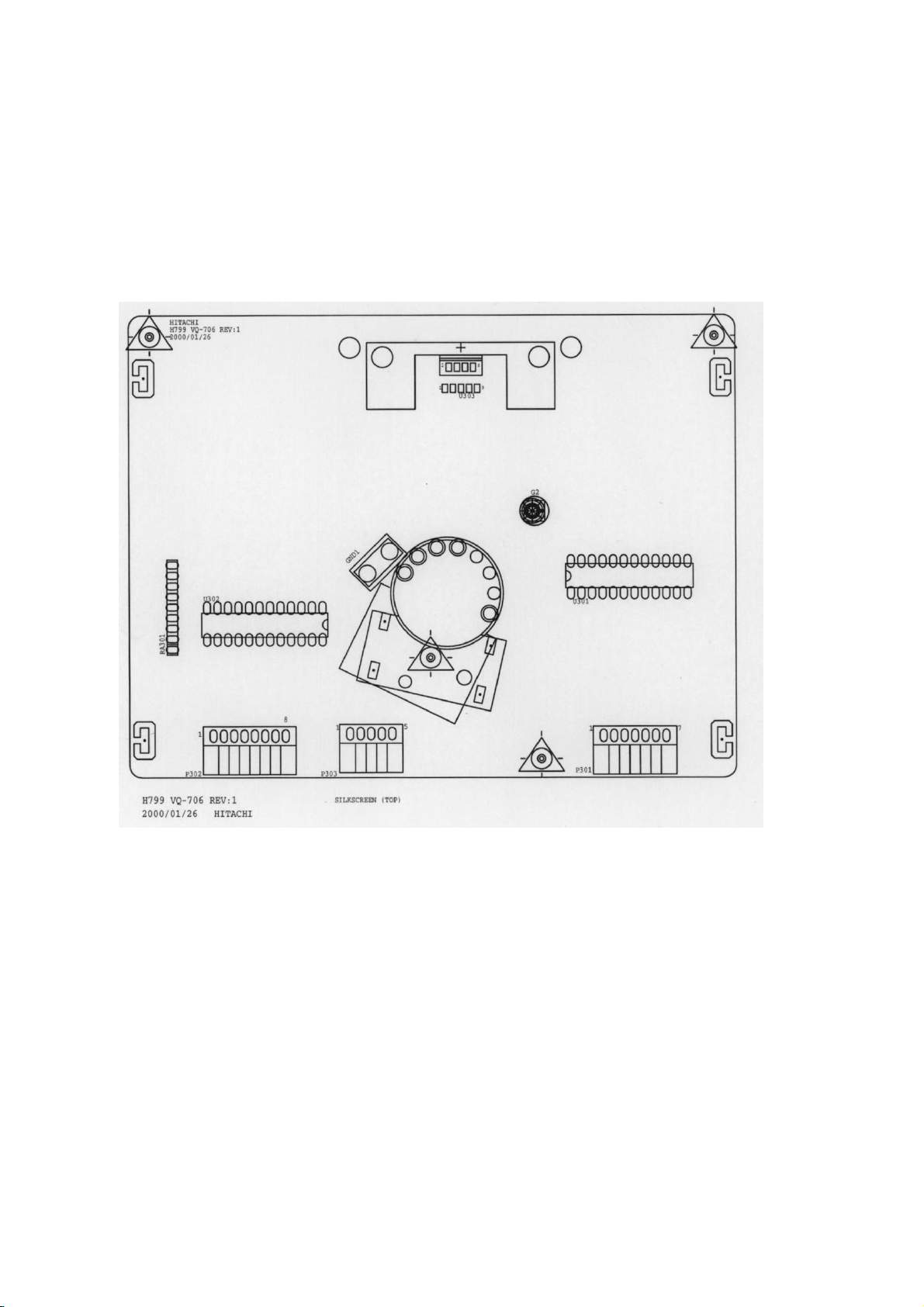
2. CONTROL AND CONNECT LAYOUT
Main PCB
9
Page 11
B. Video PCB
10
Page 12
C. Pin Assignment
C-1. Connect Function
VR501 : H-CENTER VR
P701 : TILT CONN
P8 : CANCEL COIL CONN
JP1: PRESET CONN
P902 : DEGAUSSING COIL CONN
P703 : X-RAY TEST PAD
-
1
2
3
4
5
6
12V -- GND --
7
8
P302 P303 P301 P5
HFLB Vout DSUB9 DDC-SCL
GND EEP-SCL R-IN DDC-SDA
G1 EEP-SCL GND GND
6.3V H-OUT B-IN V-SYNC
5V GND GND H-SYNC
75V -- G-IN --
CONTRAST -- -- --
11
Page 13
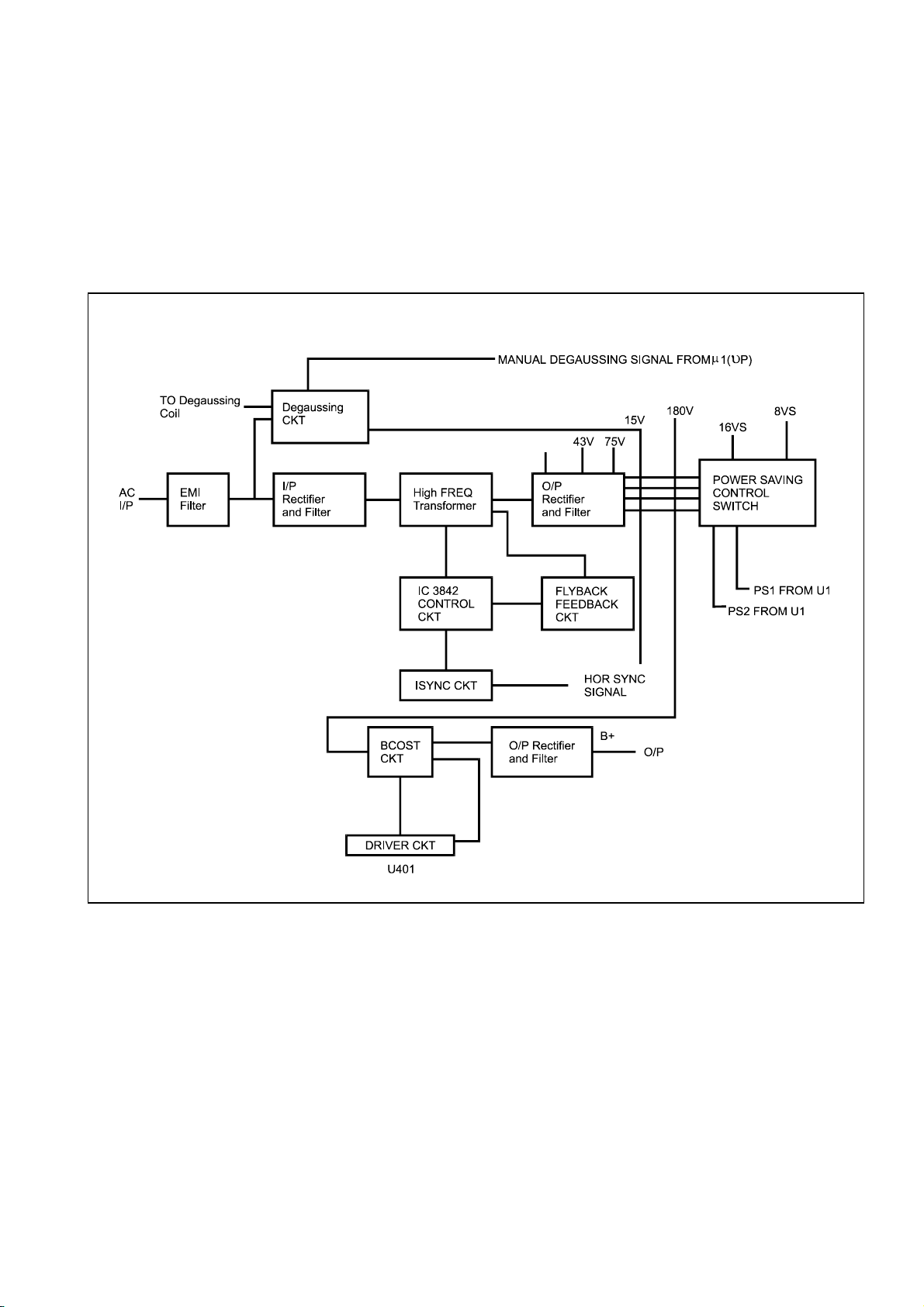
3. Power Supply Portion
12
Page 14

4. OPERATION THEOREM
A. Power Supply:
Transfer AC source to DC source that supply all the circuit power. It includes:
(1) +12V: For video pre-amp circuit, parts of horizontal and vertical deflection circuit.
(2) +180V: For deflection and H.V circuit
(3) +7.5V: For CRT heater and u-P power.
(4) +75V: For video AMP. Circuit.
(5) +42V: For vertical deflection and Horizontal predriver .
(6) +16V: For vertical preampifier
B. Deflection:
Produce YOKE deflection current of horizontal and vertical, CRT H.V and bias that makes screen raster.
C. Video
Amplify the video signal and add the signal to the cathode of CRT to produce video on the screen.
D. Digital Controllor
With the EEPROM and PROGRAM, the micro-processor(u-P) control all the picture performance.
From the key control, the user can change the H-size, V-size, R-gain.…etc.
13
Page 15

14
E. Function Block Diagram
Page 16

F. Power Supply
F-1. Rectifier And Filter Ckt:
The 90Vac-265Vac input line voltage is rectified by D901- D904, and smoothed by C906 to provide
DC operating voltage for the circuit.
F-2. Flyback And Pwm Ckt :
When power is initially applied to the circuit,C909 charges through R903, Q902.When the voltage
across C909 reaches a level of 16V, U901 is enabled, turning on Q901 and turning off Q902 to
complete start-up action.
During the On-time of Q901, energy is stored in T900. At this time the polarity of the output windings
is such that all output rectifiers are reverse biased and no energy is transferred. Primary current is
sensed by R914 and compared to a DC level that is determined by voltage feedback. When this
level is reached, Q901 is turned off and the polarity of all T900 windings reverses , forward biasing
the output rectifiers. All the energy stored is now transferred to the output capacitors. Many cycles
of this store/release action are needed to charge the outputs to their respective voltages.
The voltage across C949 is fed through a voltage divider R984,R985,R986, R987 and VR980 to the
error amplifier U980 and compared to an internal 2.5V reference ,then determine the feed back
level of U901 PIN1.
F-3. Snubber Ckt:
Energy stored in the leakage inductance of T900 cause a voltage spike which be added to the
normal reset voltage across T900 when Q901 turn off. The clamp consisting of D905, R904 and
C907 limits this voltage excursion from exceeding the Vds rating of Q901. In addition, a turn off
snubber made up of D906, R905 and C908 keeps power dissipation in Q901 low by delaying the
voltage rise until drain current has decreased from its peak value. This snubber also damps out any
ringing which may occur due to parasitic.
F-4. Synchronized Ckt:
The oscillator frequency is defined by R912 , C920. The equation is approximately : Fosc=1.8/
(R912*C920). The external signal “SYN+ & SYN−”
that comes from horizontal circuit T802 can synchronize the working frequency of power circuit Via
ZD903,R918,R919 and R916.
F-5. Power Saving Ckt:
The monitor has ON, Suspend/Standby and OFF states.The monitor enters Suspend/Standby
mode if either V-sync or H-sync signals are removed.When the machine in the Suspend/Standby
State, PS1 should be low to turn off +15Vs. In this state, input power should be less than 15W and
D960 LED illuminate yellow. The monitor enters OFF mode if both H-sync and V-sync are removed.
When in the OFF State, PS1 and PS2 should below simultaneously to turn off +15Vs and +8.3Vs
outputs. In this state, input power should be less than 5W and D960 LED illuminate amber.
15
Page 17

F-6. Degauss Ckt
The DEGU signal which comes from micro-p to control degauss coil act or not.
When DEGU is high, Q950 will be saturated to make RL901 working, AC line provides
a degaussing current to degauss coil.
F-7. OVERLOAD PROTECTION CKT
The primary current flows through the current sensing resistor R914. The voltage drop on R914 will
be rectified by D927 and keep a dc level on C927 that is dependent on the output power. When this
DC level reach the trigger voltage of Q920 , the pin1 of U901 goes low and the power stage is
immediately switched off.
F-8. BROWN – OUT CKT
When the input voltage down below the setting level (85Vac-75 Vac), Q904 will be supplied a trigger
voltage to make Q920 turn on ,and this time, power supply shall be shut down.
G. Deflection
G-1. Sync Rpocessor:
H-sync & V-sync or input to U1(u-P), then u-P output the H-out & V-out to
U401(TDA4858).
G-2. Hor. Processor & Vert. Pre-Amp
Fig.2 is the block diagram of IC TDA4858.
Hor . processor
The H-out that come from u-P will input to the pin 15 of U401,it will be compared
with the oscillator sawtooth voltage by the PLL1(pin 26) phase detector, After that, it will be
compared again with the flyback pulse (pin 1) by the PLL2. The PLL2 detector thus compensates
for the delay in the external horizontal deflection circuit by adjusting the phase of the HDRV(pin 7)
output pulse.
+
B
Vert. Pre-am
control
The U401 pin5 to pin3 is operation Amprifier from pin11 EW DRV parabla amplitude DC,H-Size
and Trapezium correction wave from connection ,pin6 is forward PWM output ,driver the
Q420,Q422 all mode B
+
is 180V
Vertical oscillator will be trigged by V-out (pin 14) .It is availvable to get sawtooth waveform in pin 24.
V-center, V-amp and V-linearity can be adjusted in pin 17, 18 and 19. The vertical output driver is
come from pin 12 and 13.
16
Page 18

LLHLL
L
L
L
LLLLHHHHHHHHHHLLLHH
H
H
H
H
H
G-3. Vertical Output
IC U601(TDA 4866) is the vertical amp IC, the output pin6 connect to the YOKE .The sawtooth
current float across the YOKE to make vertical deflection. Fig.3 is the block diagram of IC TDA4866
G-4. Horizontal Driver Circuit
The driver pulse that come from U401 pin7 drive Q417,Q416,TO Q503,then transfomer T501
convert driver pulse to driver current to drive horizontal output transistor Q504.
G-5. Horizontal Output Stage
31K → 35K → 37K → 43K → 46K → 53K → 60K → 64K → 68K
SW4
C515
SW3
C539
SW2
C521
SW1
C520
L:ACTION
17
Page 19

H. Flyback Transformer
In the primary of F.B.T ,there is about 900Vpp in the LC resonant interval,
It convert to the secondary of F.B.T to produce about 26KV for CRT anode voltage.
The other bias for CRT IS G4.G3(4∼8KV),G2(0∼1000V)and G1(-160V)
18
Page 20

19
H-1. . BLOCK DIAGRAM
Page 21

I. VIDEO AMP. CIRCUIT
I-1. VIDEO PRE. AMP.
The video pre-amp IC is U301(KA2143B). The input signal is 0.7Vpp, then pre-amp IC U301 amplify
the video signal to 4~5Vpp. The WHITE BALANCE and CONTRAST shall be adjusted by
adjustment the bias voltage of U301. Fig.4 is the block diagram.
I-2. VIDEO AMPLIFIER
The video amplifier is U303(LM2439), it amplify video signal to about 40Vpp. Video output signal
add to cathode by AC coupling. The DC bias is controlled by the output pwm of IC U302.
Fig.5 is the block diagram
I-3. BLOCK DIAGRAM
KA2143B
20
Page 22

LM2439
Simplified Schematic Diagram (One Channel)
21
Page 23

5. TROUBLESHOOTING
A. Power Supply Check
Start
Check
fuse open
Is
Q901 VDS
waveform normally?
Is 8V
in spec?
Is 15V
in spec?
Yes
No
No
No
Check and repla ce E MI Filter
and Q901, I/P Rectifer
and filter
Check and replace Q902,
Q903, U901, D908, R908
Check D940, C940, Q940,
Q941, VR980
Check D941, C944, Q942, Q943
Is B+voltage
correct?
Combine with
monitor check operating
frequency?
OK
Stop
No
No
Check D944, D945, C949, Q504,
R538, Q505
Check and replace ZD903, R918,
R919, R916, D911, C920
22
Page 24

B. Monitor Check Flow Chart
B-1. No Raster
No raster
Check power
indicator is lit
Yes
Check
contrast & brightness
control adjust to MAX.
Yes
HEATER voltage= 6.3 VDC
Check
G1=
G2=
Check CRT
-50~70 VDC
350~700VDC
Yes
No
No
F.B.T pin1
about 700Vpp
Check Q801
Check AC
power input
Yes Yes
Yes
Check Q504
collector voltage
about 900 Vpp
Yes
Check U801 pin6
square waveform
No
U801 pin7 Vcc
Check power
supply circuit
Check
power supply
circuit
No
No
Check U401
No
Check U401
pin7 output
square waveform
Yes
Check Q417, Q416
Yes
Check Q505 "S" pin
voltage 180VDC
Yes
Check T802 D506
23
Page 25

No. 0502
24
Page 26

No. 0502
25
Page 27

Schematics and PCBs Supplement
CM615ET
CM615ET302
CM615ET303
26
Page 28

H-SIZE
12V
B-DRIVE
H-DRIVE
15VS
V-OUT
H-OUT
Q814-E
X-RAY
X-RAY"
PIN
TRAP
12V
P730
V-CENT
V-SIZE
V350
2SC945
Q404
BLANCE
PARALLEL
H-PHASE
R402 100
R730
5.11K
1%
R424
47K
R405
470K
1/4W
GND
1
+
C446
470U
16V
GND
2
R731
4.3K
1/4W
1%
R441
150K
Q401
GND
RN1203
R459
10K
1/4W
2SC945
Q405
R447
470K
1/4W
R454
39K
1/4W
R416 100
D420
1N4148
R732
12K
1%
GND
2SC945
Q406
ZD730
HZ12B1
GND
R426
39K
1/4W
C730
100U
10V
2SC945
Q407
R466
680K
GND
C404
470P
GND
Q730
2SA733
+
R733
1K
R423 39K
1/4W
12V
C406
10U
25V
NP
GNDGND
1/4W
R427
47K
1/4W
2SC945
Q408
R401
240K
R403
68K
1/4W
R410
22K
1/4W
R736
C433
470P
2.2K
R734
Q731
2SC945
GND
R400
75K
2SC945
Q409
R408
160K
1/4W
10K
1/4W
C734
0.1U
D406
1N4148
D404
1N4148
1/4W
R412
FS
2.2
2SC945Q417
D405
1N4148
Q416
C401
0.01
MEF
2SA733
GND
100
10
1/4W
C424
R601
100
1/4W
.1U
MEF
R603
C444
GND
.01U
MEF
16 15 14 13 12 11 10 9 8 7 6 5 4 3 2
MEF.01UC443
+
470U
GND
R417
FS
R418
1.2K
1/4W
C408
16V
U401
TDA4858
ZD404
GND
3B1
R419
3.3K
GND
R404
6.2K
1/4W
1%
R431
C414
.22U
MEF
R429
15K
R432
976
1%
C415
.01U
MEF.22UC422
22K
1%
C412
.1U
MEF
C413
.0015U
PPN
R434
150K 1/4W
R428
GND
R440
270K
1/4W
GND
R465
56K
1/4W
+
C456
4.7U
2SC945
Q413
2SC945
Q410
2SC945
Q411
R444
330K
1/4W
GND
R496
12K
R496A
6.8K
1%
2SC945
Q412
1%1.82K
PPN
2SC945
Q414
220
D491
15V
FR104
1%
U403
LM358
6
5
R413
27.4K
GND
1%
7
+
R469
200K
1/4W
R471
D494
C427
100U
16V
R494
56
1/4W
C512
.1U
250V
MEF
FORM U401
PIN 26
R468
10K
2
-
3
+
R461
33K
1/4W
1
C432
.1U
1N4148
+
GND
D430
1N4148
D431
1N4148
GND
18.2K
R480
10K 1/4W
R472
10.2K
GND
1%
1/4W
R491
C491
GND
R449
47
R451
2.2K
1/4W
+
470U
GND
1/4W
16V
2SC945
Q422
2SA733
1/4W
Q420
ZD491
HZ12B1
C437
100U
16V
+
1%
1/4W
R464
2.94K
2SA733
Q424
C428
4700P
PPN
2%
GND
VR405
20K
C410
.01U
MEF
GND
R430
10K
+
GND
C411
100U
16V
5.36K
GND
R421
1%
R411
13K
1/4W
D403
FR104
1%
7.5VS
FBP
R422
R437 620K
32313029282726252423222120191817
R420
C416
R407
2SC945
Q438
R409
1M
GND
MEF.01UC438
27K
MEF.01U
13K
1/4W
1.5K
1/4W
FS
U601
MEF.012U
TDA4866
2.2M
R606
10K
1/4W
R612
10
1/4W
R614
1/2W
FS
R436 56K
C417
R406
C448
.1U
MEF
R607
3.9
2W
+
C603
2200U
25V
GND
R604 1W1
C604
100U
63V
+
43V
C434
.01U
MEF
ZD442
HZ12B1
R482
4.7K
R481
10K
R442
4.7K
R443
3K
1/4W
Q442
2SD667
GND
C435
MEF.22U
250V
47
C611
.22U
MEF
HFLB
V-OUT
G1
GND
+
C420
10U
16V
R611
160
1/2W
987654321
R602
2.94K
1%
L611
100uH
P501
R609
2.7K
1/4W
1
2
3
4
R613
10
1/4W
+
GND
D612
1N4148
R610
12K
C605
1U
43V
D611
1N4148
+
C606
2.2U
GND
GND
15VS
V-DF
NO NOTES ? W RESISTOR IS 1/8W
No. 0502
Deflection & Power - 1
27
Page 29

43V
H-DRIVE
C501
47U
63V
D507
BYD73A
DGQ503
2SK941
S
GND
T501
GND
+
GND
R503
240
7W
C502
.22U
MEF
R510
100
1/4W
R509
10K
1/4W
GND
C531
3300P
PPN
R508
560
1W
GND
Q504
2SC5408
GND
L504
BEAD
C505
6800P
2KV
MPM
P501
YOKE-H
1
2
3
4
R517
10K 1/4W
Q505
IRF9634
SD
G
GND
C507
4700P
500V
P802
R802
10
P803
1
2
(R)2.2 2WR512
(R)2.2 2WR514
R513
22
1/2W
GND
D502
BY329
1500V
GND
C506 2KV180P
R813
2.2
L508
BEAD
D506
BYV26C
FBP
1/4W
FS
11
T802
2
6
4
7
12
9
10
8
L503
R515
2.2
1/4W
R516
2.2
1/4W
D503
HER102
C555
330P
D504
HER102
C554
330P
105C
C562
220U
16V
C561
220U
16V
105C
+
VR501
5K
R501
+
1K
Q522
2SD667
Q521
2SB647
R561
10
1W
SW4
15VS
SW1
SW2
180
X-RAY"
FBP
TILT
7.5VS
ABL
5V
CONT
R704
2.2
1/4W
FS
R705
10K
C812
.01U
MEF
R702
2.2K
1/4W
D817
1N4148
R819
10K
1/4W
U403
PIN7
R817
R701
2.2K
Q703
2SC945
GND
R537
R818
3.3K
1/4W
C703
10U
25V
7.5VS
Q519
C945
C803
GND
D420
C829
Q816
2SC945
1/2W
C513
1200P
1KV
+
22U
C809
47U
25V
+
R522
470
GND
R831
10K
D810
1N4148
+
GND
GND
R832
4.7K
P8
1N4148D519
1N4148D520
BYV36C
5
76
2
1
L501
4510
2.75UH
D803
U801
KA3842A
C814
2.2U
C511
.39U
400V
MPP
348
1
2
2SB647AC
GND
UPABL
+
GND
R549
2.2K
1/4W
Q510
RN1206
GND
R524
2.2K
1/4W
R536
2.2K
R521
1/4W
2.2K
1/4W
12KR520
R519
12K
Q516
BF421
1/4W33K
FS
1/2W100
GND
R538
+
C524
4.7U
250V
Q803
2SC945
1.2
2W
Q508
RN1206
GND
R539
100
1/2W
R816
220
1/4W
Q509
RN1206
GND
R502
.2
1W
FUSE
L506
100UH
100U
250V
105C
D808
1N4148
GND
GND
Q701
2SC945
+
GND
2SA733
Q702
GND
BEAD
C701
10U
L90
25V
GND
P701
TO ROTATE COIL
+
R814
10
2
1
L89
BEAD
R830
10K
1/4W
CONTRAST
D821
Q806
R821
22K
1N4148
R822
100K
1/4W
Q545
R815
470
1/4W
R806
680K
C821
1000P
GND
R546
C539
.1U
2200P
GND
D815
1N4148
36
2W
C810
R541
10K
1N4148D541
BYV36C
GND
Q546
2SA733
C516
.01U
GND
D804
R820
1K
1/2W
C801
2700P
1.6KV
MPM
GND
R812
12K
R545
4.7K
R804
10K
1/4W
G
R544
22K
U403-P7
D542
FR104
D
S
R811
150
1/4W
D823
1N4148
C515
1U
Q517
IRFS640A
D802
UF5408
GND
R823
100
R803
1K
R826
10K
C532
.01U
G
MPP250V
R530
100
1/4W
D
S
GND
D526
FR104
IRFS630A
D801
BYM36E
Q801
3N90
R801
0.3
2W
(R)
GND
Q514
R531
10K
C834
.01U
GND
R535
D527
FR104
G
R533
22K
C521
.47U
L502
250V
MPP
R534
47
5W
+
C522
D
S
3.3U
250V
Q515
IRFS630A
R827
470
1/2W
C520
.22U
250V
MPP
D532
1N4148
D
G
R532
S
10K
C534
.01U
T801
2
1
14
12
7
44
5
8
9
10
+
C846
2.2U
105C
GND
Q805
2SC945
R834
1K
+
R825
C820
33U
1/4W
GND
VR802
20K
GND
C835
.1U
MEF
GND
+
C510
47U
250V
1
2W
91K
C523
.1U
250V
MPP
R807
D505
1SS82
47
2W
S
R540
4.7K
1/2W
GND
D805
HER103
C806 1KV330P
D806
UF4006
2SA733
GND
B-DRIVE
T506
GND
C826
2200P
1KV
GND
R805
56
1/2W
MOF
D807
UF4006G
R852
330
1W
C.N
NO NOTES ? W RESESTOR IS 1/8W
NO NOTES ? V CAPACITOR IS 50V
C807
330P
1KV
+
C817
L509
BEAD
GND
R861
120K
1/2W
GND
Q812
2SC2271
R844
6.8K
Q813
2SC945
R847
160
GND
R846
300K
R860
470K
1/2W
R845
33K
+
GND
R843
GND
C827
2.2U
22K
C828
10U
25V
+
V-DF
HV
X-RAY
D809
R810
2K2
1/4W
1N4148
R833
33K
1/4W
R850
620K
1/2W
R824
220K
1/2W
D521
FR104
10K
GND
R848
9.1K
1/4W
R849
GND
+
C833
47U
25V
R836
2SA733
R835
4.7K
22K
Q814
VR803
10K
Q810
BF421
GND
R837
470
C825
GND
.1U
ZD801
HZ6B2
Q811
RN1206
GND
R838
180K
R839
150K
50V22U
ZD805
30-2
C818
+
2.2U
400V
105C
+
C819
22U
250V
15VS
MUTE
D420
BRI
G1
No. 0502
Deflection & Power - 2
28
Page 30

D4
4148
8.4V
GREEN
V350
MUTE
R65
1.3K
8.4V
SW1
POWER ON/OFF
PT-002-B2
SW2
PAGE
PT-002-B2
SW3
FU/ADJ +
PT-002-B2
SW4
FU/ADJ -
PT-002-B2
GND
R9
100
1/4W
R10
470
ZD1
HZ5C1
15VS
C13
47u
25V
JP1
33P
2
1
U4
+
5.1K
R5
2.7K
R6
3.6K
5.6K
C7
4148
7.5V
4148
R11
1/4W
GND
KEY-IN
R4
R7
D1
R63
10K
D2
1K
I
33P
C5
GND
PS1
4148D5
G
KIA7812
GND
9.31K
C70
4.7u
C42
1000P
Q2
2SC945
GND
O
R8
1%
C6
8MHz
KEY-IN
FAT.
+
GND
12V
+
C14
220u
16V
33p
Y1
M
DEG.
27KR70
PS2
SW1
100u
10V
4.7K
GND
HSIZE
RESET
R64
1M
ZD2
HZ5C1
C9
R1
+
C4
10u
16V
1
DAC2
U1
DAC1
DAC0
RESET
5
VDD
GND
OSCO
OSCI
P15
10
P14
P13
P12
AD1/P11
AD0/P10
15
INTE/P16
P27
P26
P25
P24
P23 P22
NT6861
EEP-SDA
EEP-SCL
+
GND
C10
.01u
8
7
U2
24C08
2
1
GND
RA2 10KX6
VSYNCI
HSYNCI
HSYNCO
VSYNCO
DAC13
DAC12
DAC11
DAC10
DDC-SCL
DDC-SDA
R13 1/4W100
6
54
3
DPA8KEE
DAC3
DAC4
DAC5
DAC6
DAC7
DAC9
DAC8
P20
P21
R14
100
U3
KIA7805P
O
G
GND
10K 1/4WR43
44K
LH
44.1K-
I
C1
.01u
GND
31K-33K
SW4
SW2
SW1
1/4W
1/4W
10K 1/4W
R45
1/4W
10K
10K
R46
10K
4.7K
R47
R50
R48
R49
4.7K
R17
33.1K36K
L
L
L
36.1K40K
L
L
H
40.1K-
L
H
52K
HH
L
HL
52.1K62K
H
H
62K-68K
H
H
HL
+
GND
C8
220u
10V
5V
C3
.01u
GND
RA1 10KX8
+
GND
C2
220u
10V
8.2K
R68 10K
R69 10K
40
VSYNC
HSYNC
VCENT
PIN.
TRAP.
TILT.
35
SUB-BRI. UPABL
(POSITIVE)
H-OUT
(NEGATIVE)
V-OUT
100 1/4W
100 1/4W
10K 1/4W
10K 1/4W
10K 1/4W
100 1/4W
2K 1/4W
R20
R21
R22
R23
R24
R25
R26
R71
120K
GND
CORNER
30
25
2120
PARA.
BALA.
BRI.
CONT.
SW4
SW2
10K 1/4W
10K 1/4W
10K 1/4W
10K 1/4W
R16 100
100
R15
1/4W
220PC39
GND
5V
DDC-SCL
DDC-SDA
4148D6
4148D9
GND
R28
R29
R31
R32
4.7uC17+4.7uC18
4.7u
4.7uC29+4.7uC30
+
4148D8
4148
220PC36
D7
GND
GND
+
C25
4.7uC16
4.7u
+
+
+
4.7uC20+4.7uC19
C15
GND
4.7uC24
4.7u
+
+
+
C23
R59
KEY-IN
GND
7.5VS
R100
P2
1
2
L30
BEAD
HFLB
GND
G1
6.3V
5V
75V
12V
CONTRAST
P1
1
2
3
4
5
6
7
8
V-OUT
EEP-SDA
EEP-SCL
H-OUT
GND
P3
R62
4.7K
470PC27
4.7K
D11
4148
D13
4148
R58
10K
GND
R57
10K
Q5
1
2
3
4
5
DDC-SCL
DDC-SDA
GND
V-SYNC
H-SYNC
P5
1
2
3
4
5
2SC945
R61
10K
GND
R60
10K
Q4
2SC945
GND
D10
4148
GND
D12
4148
H-SYNC
C37
220P
V-SYNC
3.9
2W
H-SIZE
H-PHASE
V-SIZE
V-CENT
PIN
TRAP
TILT
PARALLEL
BALANCE
AMBERAMBER
BRI
CONT
C38
220P
GND
No. 0502
Deflection & Power - 3
29
Page 31

P901
IX-0342-P
1
2
3
L
N
C910
222Y2
C903
NC
1MR901
F901
T3.15A
250V
CHS GND
20mHT901A
C904
NC
1/2W
RT901
15SP008
PR901
9
2
1
P902
DEGAUSS
RL901
OSA-SS-212DM5
D950
4148
Q950
RN1206
3
GND1
R950
1/2W75
+
C951
GND1
BD901
GBU4J
+15VS
R951
1/2W(S)
1/2W(S)
DEGU
R923
620K
R924
620K
R917
33K
+
C906
220U
400VA
GND5
R929
100K
D907
4148
C915
1U
R900
1W(F)0.2
Q902
KSP44
R972
D970
C921
+
4.7U
C923
101J
+
Q970
ZD902
HZ9A2
GND5
R921
4.7K
Q904
A733K
R903
82K
3W(S)
A
K
Q920
BT169D
GND5
R922
10K
R915
10K
C922
102K
C924
47U
16VA
R
GND5
D913
4148
R912
C917
104Z
C920
332K
R916
47
R925
1M(S)
1/2W
R926
1M(S)
1/2W
+
GND5
C909
100U
25VB
27K
1/4W
GND5
R971
R909
1/4W47
R928
4.7K
ZD901
HZ20-2
+
GND5
U9013842A
D911
4148
Q903
C945P
D908
FR104
GND5
R904
47K
2WR
Q901
2SK2761
R920
10K
GND5
D927
4148
+
C927
47U
16VA
GND5
1367
2548
R919
1/4W470
G
R927
100
1/4W
R914
0.33
2WR
#3WR.S
R908
10
1/4W(F)
C913
102K
D
S
GND5
R911
1/4W
R910
4.7K
ZD903
HZ5C1
R918
1K
1/4W
C907
103
1KV
D905
FR107
L903
BEAD
HQ901
GND5
D906
1K
C925
103
1KV
NC
GND5
GND5
C914
102K
SYN+
SYN-
C905
103
1KV
C908
NC
R905
NC
GND5
8
7
6
1
2
4
U900
3
TLP721F
C900
C90A
C960
T900
1
2
472Y1
472Y1
472Y1
KA431Z
101K
13
HD944
9
11
12
R94A
0.2
1WR(F)
10
14
15
16
R989
3K
U980
1KV
UF5408
GND1
R94B
0.2
1WR(F)
R94C
1
1WR(F)
GND1
R980
1K
R981
K
A
GND1
C992
D944
C990
101K
1KV
UF4006G
C994
471
1KV
C981
224
MEF
47
R
D943
D942
ER106
HD941
D940
ER202
C940
1000U
16VB
D930
FR104
C930
1000U
16VA
C993
D945
UF5408
R990
100
2WR
D941
ER302
R994
10
1/4W(F)
+
GND1
R984
51K
1/2W
R985
51K
1/2W
R982
1K
GND1
101K
1KV
+
R986
1.3K
1/4W
VR980
R987
470
1/4W
C987
224
MEF
250V
B201
+
250VB
GND1
GND1
+
C946
100U
GND1
63VA
+
C944
1000U
GND1
25VB
C949
100U
+
C947
47U
100VA
R944
4.7K
Q940
B772Q
R941
4.7K
1/4W
L941
5UH
D951
4148
AMBER
Q942
B772Q
R945
1.2K
1W
R942
1K
1/4W
RN1203
GND1
Q960
D946
1N4002
+
C941
100U
25VB
GND1
R961
620
1/4W
+
C943
10U
100VA
GND1
Q941
RN1203
22U
AMBER
C942
103
1KV
GND1
L940
RN1203
5UH
+
C948
50VA
LYSG3393/R7
LED1
321
GREEN
GND1
GND1
Q943
R949
47K
D949
4148
P960
R940
100K
1/4W
GND1
R962
620
1/4W
B3B-XH-A
Q961
RN1203
179V
75V
43V
15V
15VS
PS1
7.5VS
PS2
8.4V
GREEN
No. 0502
Deflection & Power - 4
30
Page 32

No. 0502
DEFLECTION & POWER BOARD - VA 717
31
Page 33

1
U303
G2
D
N
G
U302
PA301
P302
1
P303
1
SWITCH BOARD
1
U301
VIDEO BOARD
- VQ 602
SOCK1
P301
1
No. 0502
- VR 717
VIDEO & SWITCH BOARDS
32
Page 34

Schematics and PCBs Supplement
CM615ET321
33
Page 35

+5V
+8V
C1
47U
16V
GND
+
GND
OSD-SDA
OSD-SCL
SW4
VOLUM-
SW3
VOLUM+
SW2
FUNCTION
SW1
POWER-SW
U3
78L05
LED-3
D1
1N4148
I
G
C5
.01U
LED1
O
GND
G-ON
A-ON
C2
100U
16V
1
2
3
24LC08
GND
U2
< 70K
H
H
L
H
HH
SW 1
SW 2
SW 3
< 33K 52~57K41~51K36~40K33~35K 58~65K
L
L
L
L
L
L
H
LHH
H H
L
HL
SW 4
FOR 70K TABLE FOR 87K TABLE
+
C3
.01U
8
7
6
54
C85
100P
GND
GND GND
GND
R2
100
P1
1
2
3
4
5
6
7
R34
4.7K
C13
10U
16V
C86
100P
R3
100
C6
.01U
R1
10K
+
R4
GND
10K
D3
1N4148
D2
GND
R5
*
33P
GND
P101
C8
PS1
10K
1
2
3
4
5
6
7
R18
10K
CONTRAST
12MHZ
Y1
C7
JP2
GND
MODEL
PS2
R6
10K
R28
10K
GND
33P
R7
330
R32
10K
TILT
R26
10K
R8
330
R33
R25
2.2K
10K
OSD-SDA
OSD-SCL
Q5
C945
MUTE
R29
10K
R30
2.2K
R31
2.2K
1
2
DA1/P5.1
3
DA0/P5.0
4
RESET
5
VDD
6
VSS
7
X2
8
X1
9
ISDA
10
ISCL
11
STO/P4.2
12
P2.2/AD2
13
P1.0
14
P1.1
15
P3.2/INT
16
P1.2
17
P1.3
18
P1.4
19
P1.5
20
P1.6 P1.7
U1
WT62P1
MTV212
+5V
R37
10K
Q2
A733
Q1
A733
GND
3.3K
R10
1K
R9
U-LOCK
+
C12
4.7U
50V
GND
VSYNCDA2/P5.2
HSYNC
DA3/P5.3
DA4/P5.4
DA5/P5.5
D8/HALFH
D9/HALFV
HBK/P4.1
VBK/P4.0
D7/CLAMP
DA6/P5.6
P2/DA13
P2/DA12
P2/DA11
P2/DA10
P2.0/AD0
P2.1/AD1
P103
2
1
FACT/USER
R38
10K
P104
1
2
3
4
5
6
7
8
HSCL
HSDA
R35
10K
40
39
38
37
36
35
34
33
32
31
30
29
28
27
26
25
24
23
22
21
GND
AFC
GND
G1
HEATER
+5V
+100V
+12V
ABL
R41
2.2K
A-LOW
G-LOW
R36
10K
GND
SW 1
SW 2
SW 3
SW 4
P105
GND
R40
1K
1
2
3
4
5
C90
.1U
250V
R24
10K
L
L
L
L
GND
+
4.7U
GND
JP1
OSD
GND
P102
1
2
3
4
5
6
V-OUT
OSD-SDA
OSD-SCL
H-OUT
GND
R23
10K
+
C11
4.7U
50V
C14
50V
GND
L
L
L
H
ZD3
HZ5C1
GND
C17
DETECT
DDC-SCL
DDC-SDA
V-SYNC
H-SYNC
GND
C15
220P
GND
GND
C18
ZD1
HZ5C1
GND
+5V
GND
L
L
L
H
H H
H
HZ9C1D82
R21
10K
+5V
GND
HZ5C1
GND
HZ5C1
H
R20
10K
ZD4
D81
C16
1000P
GND
GND
>75K62~75K58~61K51~58K45~51K40~45K34~40K34K<
HHHH
L
H
L L
H
H H H
L
H H
H
P103 & (+) & (-) =>POWER CORD ON ==INI
R19
10K
R22
10K
R17
*
R16
*
R15
2.2K
C66
150P
GND
GND
+5V
D80
GND
C9
470P
R11
10K
R12
4.7K
ZD5
1K
*
C19
*
GND
R13
1K
R14
4.7K
Q3
2SC945
GND
R27
*
Q4
ZD2
HZ5C1
GND
RN1203
GND
R66
3.3
1W
GND
R67
JUMP
G1-ADJ
SH-SIZE
DEGAUSS
SUB-BRI
+
C10
4.7U
50V
DDC-SCL
DDC-SDA
DETECT
+5V
HSYNC
BRI.
VSYNC
HSYNC
H-OUT
V-OUT
SW3
SW2
SW1
VSYNC
+8VS
HEATER
No. 0502
Deflection & Power - 1
34
Page 36

+15VS
HDRV
+15VS
SW4
SW3
SW2
SW1
+15VS
TILT
C521
-12V
SH-SIZE
SMOD
A
GND
R548
300K
OSD-SCL
OSD-SDA
H-OUT
V-OUT
+12V
U-LOCK
C512
2.2U
16V
+
R418
100
R419
100
C418
100P
C501
100U
25V
GND
C506
1000P
R516
10K
D509
1N4148
1MR427
R547
820K
C523
.022U
MEF50V
C401
+
C402
100U
.01U
25V
GND GND
C419
100P
GND GND
100
R402
1/8W
100
R401
1/8W
R417
10K
GND
R508
2.2K
Q504
RN1206
3.3KR532
U402
7812
1 1098765432
+
2SC945
I
VFOCUS
H/HVIN
R509
2.2K
RN1206
GND
R517
4.7K
R518
2K
Q505
1N4148D511
D401
1N4148
G
Q503
20KR525
O
C403
100U
C405
100U
VSYNCIN SDA
16V
16V
GND
R538
GND
C507
.01U
*
+
C508
4.7U
SCL
HLOCKOUT
R565
*
Q521
50V
R533
3.3K
+
+
& VBLK
C831
*
250V
MPP
D859
C430
.01U
GND
Q401
2SC945
GND
*
R430
3.3K
1/8W
R504
R505
R506
1.5
D502
R546
4.7K
*
1W1.5
1N5817
R539
*
R514
10K
1W
GND
R543
22
1/2W
+15VS
R421
10K
+
C416
GND
GND
RL801
D508
1N4148
R570
22
*
C810
.01U
R515
R526
Q501
2SC5521
18.5Ts
47
Q514
2SC945
C515
.01U
100
D520
1N4148
R536
GND
MUTE
P802
L801
R529
680
5W
1
2W
C809
250V
R535
2W
GND
R410
4.7K
C527
22P
+15VS
R604
1.1k
R605
4.3K
1%
P801
H-DY
2
1
L803
6mH
1U
MPP
GND
IRFS640A
1
GND
R601
1%6.2K
R602
1%
L802
C509
330P
500V
Q513
GND
R528
*
FUSE
GND
12.5Ts
R806
100
1W
R807
47
1W
R527
10K
1W6.8
R614
1/2W
FUSE
-13V
C805
2200P
1KV
R805
330
1W
C817
*
C806
.33
400V
MPA
C417
C601
.01U
1
C803
.0068U
1KV
MPM
L501
145uH
L502
BEAD
D501
ER304
BYM36C-798
47U
16V
C609
.01U
GND
D802
L804
BEAD
+
GND GND
GND
R603
2.43K
1%
+
C602
470U
25V
L806
BEAD
C801
.0075U
1.6KV
*
.033U
GND
R530
2.2K
.047U
250V
R422
7
U601
TDA8172
1
MPM
C802
1KV
MPM
D801
C023M-15
+56V
B+
C511
MEF
GND
10K
Q402
2SC945
2
6
4
C604
.01U
GND
C510
47U
+
250V
Q508-B
R423
10K
FR10-04
+
3
5
+
GND
R424
10K
Q403
2SC945
D601
C603
100U
50V
R606
*
C605
1000U
16V
D805
UF4001
C812
+
47U
50V
R802
10
321
GND
1N4148D405
R801
10
R540
470K
1W
D522
*
+12V
D602
1N4148
R607
D806
UF4001
C813
47U
50V
P803
GND
R571
R572
P804
1
R838
1K
GND
1%
D406
1N4148
2.2
C606
.22U
MEF
+
*
*
2
R837
53.6K
1%
R608
270
1/2W
1%
R609
1W
GND
FBT
R809
GND
ZD402
HZ5B1
1
10
FUSE
G1
R836
10K
56.2K-798
C431
47U
16V
D809
R828
45.3K
1%
C607
.001U
50V
MEF
YOKE
V-DY
GND
FR105
+12V
+
GND
*
W115
D810
GND
R425
R426
3.3K
GND
2.2
FR10-04
C824
1U
50V
R829
8.2K
VR801
B2K
12K
GND
GND
R839
*
1/2W
D816
FUSE
R610
R611
10K
*
C825
*
160V
-150V
GND
+
GND
ZD401
HZ9A2
2SA733
10K
C818
22U
+
250V
Q404
+60V
GND
SG2
H.V.
G4
G2
D-FOCUS
R808
100
1/2W
FUSE
*
+
GND
+100V
R612
22K
Q601
BF420
GND
D807
UF4007
UF4007
R834
39K
R832
12K
C608
.1U
250V
MEF
R613
47K
GND
D820
100V
SG3
*
Q807
BF423
C842
22U
.068U
GND
SG1
1.5KV
+
R810
1K
C814
MEF
R872
2.2M
R871
2.2M
R870
2.2M
R847
15K
1/2W
Q843
2SD667
R849
22
R860
1/2W
C861
1000P
D-FOCUS
R833
820K
R830
220K
1/2W
R831
10K
470
1KV
R861
150K
1/2W
R811
20K
C815
.022U
MEF
C816
.015U
1KV
PPN
GND
C840
D841
1N4148
R84847R846
C843
100V
Q850
BF423
R855 470K
-150V
+
10U
1U
V-OUT
R812
2SA733
GND
R822
470
C822
120P
2SA733
R842
3.9K
1N4148
6
4
C855
C852
50V
10K
Q808
R819
1/8W
Q840
R843
36K
D840
47
+
8
2u2
16V
1U
GND
15K
R817
100
1/8W
C821
1U
50V
2SC945
2SC1627
T801
11 0
R851
4.7K
+
R854 18K
C854
10U
+
100V
C853
+
50V
1U
R820
150K
R827
47K
R835
100
D811
1N4148
R813
2.2K
NP
Q820
Q841
2SB647
+
R823
10K
R844
1.2K
C841
.01U
R845
100
Q842
C851
100V
R853
5.6K
R852
2.7K
BRI.
G1-ADJ
+12V
SMOD
R816
22
1/4W
FUSE
R818
39K
R821
820
47U
G1
+
R856
1.2K
SUB-BRI.
CONTRAST
FOCUS
+
C820
100U
16V
+56V
V-DY
ABL
G2
+12V
R537
R501
R534
*
Q517
*
6.8
1W
C504
1U
+
R542
*
2W
6.8
1W
R531
100
C505
2200P
D503
GND
1N4148
C807
.27
400V
MPP
R507
10K
GND
C502
.47U
MEF
50V
R850
470K
1/2W
R502
150
1W
C503
.01U
Q502
2SK941
GND
R556
*
Q810
D505
R557
1K
R558
1K
D504
1N4937
IRFS630A
R510
22
R511
10K
*
Q518
*
D514
*
1N4937
Q809
C514
.1U
R512
D513
IRFS630A
22
R513
10K
C513
.1U
*
D510
1N4148
C808
.15
400V
MPP
D521
*
T501
D515
+56V
R857
470K
1/2W
R563
*
*
*
C531
*
GND
Q831
R564
*
R541
*
SMOD
HEHTCOMP
ISENSE
R409
1/8W
R407
1N4148
D402
1N4148
2SA733
GND
R411
270K
1/8W
1%
R412
100K
1/8W
GND
1K
D404
Q511
2SC945
Q512
1%10K
GND
R403
10
FUSE
C404
.01U
VCC
FC1
C410
.1U
50V
MEF
D506
1N4148
Q506
2SC945
Q507
2SA733
D507
1N4148
C520
1000P
.022U
GND
R406
3.3K
1/8W
B+OUT
PLL2C
C409
50V
MEF
C530
.22U
MEF
C522
4.7U
16V
R545
2.2K
R405
GND
C0
C414
1000P
50V
MEF
L805
+12V
120uH
P501
1
2
R519
560
R520
1/2W
82
2W
GND
Q508
2SA733
R521
3.32K
NP
1%
R524
22.1K
1%
Q509
2SA733
GND
R523
18.2K
1%
R522
1K
1%
GND
Q802
2SC1213
2SB857
C811
2.2U
63V
MEF
Q801
R548
*
R549
*
GND
Q510
*
GND
GND
JP-ST
HDRV
1K
GND
HOUT
HGND
GND
R416
4.5K
1%
C411
.01U
50V
MEF
R404
4.3K
1/8W
GND
XRAY
EWOUT
VOUT
.22U
VCAP
C420
50V
MEF
C421
.47U
50V
MEF
GND
VGND
VGACAP
TDA9112
H Position
HV Focus
HFLY
C425
47U
16V
C426
.01U
+
HREF
C406
1000P
50V
MEF
PLL1F
R0
R415
1.8K
C412
+
4.7U
16V
C413
+
10U
16V
C528
220P
C424
47U
16V
+
VRB
COMP
R408
C407 1000P
.022u
PPN
GND
181920212223242526272829303132
82K
1/8W
VEHTCOMP
REGIN
R420
220K
1/8W
C408
17
161514131211
FOCUS
No. 0502
Deflection & Power - 2
35
Page 37

D901
1
1
F901
T3.15A
250V
L
1N5406*4
D902
420035mH
C902
X20.47U
L901
420035mH
C901
X2.22U
R901
1M
1/2W
CHS GND
GND2
3
2
1
P901
D903
4
32
4
32
L902
N
D904
RT901
SP15008
C934
332Y2
GND2
GND2
C927
472Y2
RL901
1
P902
C960
R963
GND1
1/2W
5
1
R964
3
R981
1/2W_F
6
1/2W_F
C924
22U
50V
+
GND5
R929
100K
1/4W
+13.5V
R926
1M
1/4W
+
C906
220U
400V
GND5
R960
56K
Q903
C945
GND5
D914
1N4148
0.2
GND5
R902
1W
R928
1/2W1M
ZD960
NC
R961
NC
Q960
R927
1M
1/2W
NC
Q930
BT169D
D913
1N4148
R962
NC
D960
NC
A
KG
GND5
ZD930
HZ20-2
R910
10
1/4W
C932
104Z
GND5
R903
33K
1W
Q902
KSP44
R909
1/4W10
D910
R936
R932
20K
GND5
4148
R920
10K
1/4W
1K
R904
D905
FR107
Q901
2SK2761
R907
0.33
3W_S
GND5
D930
1N4148
+
C930
100U
25V
GND5
47K
2W
HSQ901
GND5
R930
240
1/4W
L903
BEAD
GND5
C907
.01U
C908
1KV
C925
.01U
1KV
D906
NC
1KV
NC
GND5
472Y1
T901
ERL39
11
14
R905
NC
2W
GND5
R950
75
1/2W
PR901
D950
1N4148
+
GND5
DEGU
Q950
3
2
C945
C952
100U
25V
GND1
R951
+
4.7K
1/4W
GND1
R931
1M
D921
1N4148
U901 3842
C917
104Z
1/4W
D922
+
FROM
F.B.T
C923
10U
50V
R919
1/4W
82
1N4148
GND5
C916
333J
MEF
GND5
D911
1N4148
D912
1N4148
C909
220U
25V
R912
27K
1/4W
C912
332J
PEN
R918
47
1/4W
D908
FR104
GND5
1367
2548
C913
102K
C922
102K
R908
2.2
1/4W
1/4W
R922
10K
C914
102K
R923
4.7K
1/4W
R911
1/4W1K
4
3
9
C928
330K
16
GND5
472Y1
U900
LTV817M-B
C900
1
2
7
2,8
4
GND1
R983
10
1/2W_F
R974
1K
1/4W
R975
3K
U904
KA431
NC
D943
UF4006G
200VB
D942
ER306
NC
HS941 NC
10
D940
UF5402G
R982
10
D944
FR104
SF24G
D970
330P
1KV
C977
224J
MEF
K
R
A
GND1
C963
1KV
C947
47U
C962
NC
C981
330P
1KV
C983
NC
HS942
NC
D941
ER302
C982
330P
1KV
R977
47
+
GND1
VR901
200B
R954
1/2W
GND1
R973
470
1/2W
C975
0.068
250V
MEF
R976
1K
1/4W
L941
5UH
NC
+
C946
470U
100VB
GND1
+
C944
1000U
25VB
GND1
+
C940
1000U
16VB
GND1
+
C970
1000U
+
25VB
GND1
C949
1000U
16VB
R972
2.26k
1/8W
MF
R965
NC
1/4W
R970
27K
1/2W
R971
22K
1/2W
GND1
L942
5UH
C942
470U
16VA
R984
15K
2W_R
R944
4.7K
1/4W
JP903
+
GND1
R991
R993
NC
R941
4.7K
1/4W
JP904
NC
Q992
A733
NC
Q962
GND1
10mm
NCB649
R966
B772
5mm
Q991
D400
NC
R992
NC
1/4W
2WNC
Q942
B772
Q940
R945
R942
820
1/2W
GND1
Q961
GND1
1K
1W
RN1203
GND1
D991
R994
NC
NC
Q941
NC
Q943
RN1203
GND1
+
C950
100U
25V
R995
NC
+
C951
NC
25V
1N4148D946
R943
10K
1/4W
R997
NC
1/4W
R946
Q993
NC
+90V
PS2
+53V
+13.5V
+13.5VS
JUMP10mm
PS1
+7VS
(HEATER)
PS2
+10V
(UP)
-11V
No. 0502
Deflection & Power - 3
36
Page 38

No. 0502
DEFLECTION & POWER BOARD - VA 739
37
Page 39

U301
U201
SOCK1
P302
SWITCH BOARD
- VR 739
P301
VIDEO BOARD
- VQ709
U202
P303
No. 0502
VIDEO & SWITCH BOARDS
38
Page 40

THE UPDATED PARTS LIST
FOR THIS MODEL IS
AVAILABLE ON ESTA
Page 41

Hitachi, Ltd. Tokyo, Japan
International Sales Division
THE HITACHI ATAGO BUILDING,
No. 15 –12 Nishi Shinbashi, 2 – Chome,
Minato – Ku, Tokyo 105-8430, Japan.
HITACHI EUROPE LTD,
Whitebrook Park
Lower Cookham Road
Maidenhead
Berkshire
SL6 8YA
UNITED KINGDOM
Tel: 01628 643000
Fax: 01628 643400
Email: consumer-service@hitachi-eu.com
HITACHI EUROPE GmbH
Munich Office
Dornacher Strasse 3
D-85622 Feldkirchen bei München
GERMANY
Tel: +49-89-991 80-0
Fax: +49- 89-991 80-224
Hotline: +49-180-551 25 51 (12ct/min)
Email: HSE-DUS.service@hitachi-eu.com
HITACHI EUROPE srl
Via Tommaso Gulli N.39, 20147
Milano, Italia
ITALY
Tel: +39 02 487861
Tel: +39 02 38073415 Servizio Clienti
Fax: +39 02 48786381/2
Email: customerservice.italy@hitachi-eu.com
HITACHI EUROPE S.A.S
Lyon Office
B.P. 45, 69671 BRON CEDEX
FRANCE
Tel: 04 72 14 29 70
Fax: 04 72 14 29 99
Email: france.consommateur@hitachi-eu.com
HITACH EUROPE AB
Egebækgård
Egebækvej 98
DK-2850 Nærum
DENMARK
Tel: +45 43 43 6050
Fax: +45 43 60 51
Email: csgnor@hitachi-eu.com
Hitachi Europe Ltd
Bergensesteenweg 421
1600 Sint- Pieters-Leeuw
BELGIUM
Tel: +32 2 363 99 01
Fax: +32 2 363 99 00
Email: sofie.van.bom@hitachi-eu.com
www.hitachidigitalmedia.com
Tel: 03 35022111
HITACHI EUROPE S.A.
364 Kifissias Ave. & 1, Delfon Str.
152 33 Chalandri
Athens
GREECE
Tel: 1-6837200
Fax: 1-6835964
Email: service.hellas@hitachi-eu.com
HITACHI EUROPE S.A.
Gran Via Carlos III, 86, planta 5
Edificios Trade - Torre Este
08028 Barcelona
SPAIN
Tel: 93 409 2550
Fax: 93 491 3513
Email: atencion.cliente@hitachi-eu.com
HITACHI Europe AB
Box 77 S-164 94 Kista
SWEDEN
Tel: +46 (0) 8 562 711 00
Fax: +46 (0) 8 562 711 13
Email: csgswe@hitachi-eu.com
HITACHI EUROPE LTD (Norway) AB
STRANDVEIEN 18
1366 Lysaker
NORWAY
Tel: 67 5190 30
Fax: 67 5190 32
Email: csgnor@hitachi-eu.com
HITACHI EUROPE AB
Neopoli / Niemenkatu 73
FIN-15140 Lahti
FINLAND
Tel : +358 3 8858 271
Fax: +358 3 8858 272
Email: csgnor@hitachi-eu.com
HITACHI EUROPE LTD
Na Sychrove 975/8
101 27 Praha 10 – Bohdalec
CZECH REPUBLIC
Tel: +420 267 212 383
Fax: +420 267 212 385
Email: csgnor@hitachi-eu.com
 Loading...