

Page 1

SERVICE MANUAL
MANUEL D'ENTRETIEN
WARTUNGSHANDBUCH
CAUTION:
Before servicing this chassis, it is important that the service technician read the “Safety
Precautions” and “Product Safety Notices” in this service manual.
SM00026
CL43WP910TAN
CL55WP910AN
Data contained within this Service
manual is subject to alteration for
improvement.
ATTENTION:
Avant d’effectuer l’entretien du châassis, le technicien doit lire les «Précautions de sécurité»
et les «Notices de sécurité du produit» présentés dans le présent manuel.
VORSICHT:
Vor Öffnen des Gehäuses hat der Service-Ingenieur die „Sicherheitshinweise“ und „Hinweise
zur Produktsicherheit“ in diesem Wartungshandbuch zu lesen.
Les données fournies dans le présent
manuel d’entretien peuvent faire l’objet
de modifications en vue de perfectionner
le produit.
Die in diesem Wartungshandbuch
enthaltenen Spezifikationen können sich
zwecks Verbesserungen ändern.
SPECIFICATIONS AND PARTS ARE SUBJECT TO CHANGE FOR IMPROVEMENT
COLOUR TELEVISION
DECEMBER 1999
Page 2

ENGLISH
SAFETY PRECAUTIONS
WARNING: The following precautions must be observed.
ALL PRODUCTS
Before any service is performed on the chassis an
isolation transformer should be inserted between the
power line and the product.
1. When replacing the chassis in the cabinet, ensure
all the protective devices are put back in place.
2. When service is required, observe the original
lead dressing. Extra precaution should be taken to
ensure correct lead dressing in any high voltage
circuitry area.
3. Many electrical and mechanical parts in
HITACHI products have special safety related
characteristics. These characteristics are often not
evident from visual inspection, nor can the
protection afforded by them necessarily be
obtained by using replacement components rated
for higher voltage, wattage, etc. Replacement
parts which have these special safety
characteristics are identified by marking with a
! on the schematics and the replacement parts
list.
The use of a substitute replacement component
that does not have the same safety characteristics
as the HITACHI recommended replacement one,
shown in the parts list, may create electrical
shock, fire, X-radiation, or other hazards.
4. Always replace original spacers and maintain lead
lengths. Furthermore, where a short circuit has
occurred, replace those components that indicate
evidence of overheating.
5. Insulation resistance should not be less than 2M
ohms at 500V DC between the main poles and
any accessible metal parts.
6. No flashover or breakdown should occur during
the dielectric strength test, applying 3kV AC or
4.25kV DC for two seconds between the main
poles and accessible metal parts.
7. Before returning a serviced product to the
customer, the service technician must thoroughly
test the unit to be certain that it is completely safe
to operate without danger of electrical shock. The
service technician must make sure that no
protective device built into the instrument by the
manufacturer has become defective, or
inadvertently damaged during servicing.
CE MARK
1. HITACHI products may contain the CE mark on
the rating plate indicating that the product
contains parts that have been specifically
approved to provide electromagnetic
compatibility to designated levels.
2. When replacing any part in this product, please
use only the correct part itemised in the parts list
to ensure this standard is maintained, and take
care to replace lead dressing to its original state,
as this can have a bearing on the electromagnetic
radiation/immunity.
PICTURE TUBE
1. The line output stage can develop voltages in
excess of 25kV; if the E.H.T. cap is required to be
removed, discharge the anode to chassis via a
high value resistor, prior to its removal from the
picture tube.
2. High voltage should always be kept at the rated
value of the chassis and no higher. Operating at
higher voltages may cause a failure of the picture
tube or high voltage supply, and also, under
certain circumstances could produce X-radiation
levels moderately in excess of design levels. The
high voltage must not, under any circumstances,
exceed 29kV on the chassis (except for projection
Televisions).
3. The primary source of X-radiation in the product
is the picture tube. The picture tube utilised for
the above mentioned function in this chassis is
specially constructed to limit X-radiation. For
continued X-radiation protection, replace tube
with the same type as the original HITACHI
approved type
4. Keep the picture tube away from the body while
handling. Do not install, remove, or handle the
picture tube in any manner unless shatterproof
goggles are worn. People not so equipped should
be kept away while picture tubes are handled
LASERS
If the product contains a laser avoid direct exposure to
the beam when the cover is open or when interlocks are
defeated or have failed.
2
Page 3

FRANÇAIS
CONSIGNES DE SECURITE
AVERTISSEMENT: vous devez respecter les précautions suivantes
POUR TOUS LES PRODUITS
Avant d’effectuer une intervention d’entretien sur le
châssis, vous devez insérer un transformateur d’isolement
entre la ligne d’alimentation électrique et le produit.
1. Lors de la remontage du châssis dans le coffret,
vérifiez que tous les dispositifs de protection sont
remis en place.
2. Lorsqu’une intervention d’entretien s’avère
nécessaire, respectez l’agencement d’origine des
conducteurs. Vous devez prendre des précautions
supplémentaires pour garantir un agencement correct
des conducteurs dans toutes les zones où des circuits
haute tension sont présents.
3. De nombreux composants électriques et mécaniques
des appareils HITACHI ont des caractéristiques
spéciales de sécurité. Bien souvent, ces
caractéristiques ne sont pas évidentes lors d’un
examen visuel et la protection qu’ils offrent n’est pas
forcément garantie si vous utilisez des composants de
rechange conçus, par exemple, pour une tension plus
élevée, une puissance plus forte. Les pièces de
rechange qui offrent des caractéristiques spéciales de
sécurité sont identifiées par un repérage comportant
le symbole ! sur les schémas et sur la
nomenclature des pièces de rechange.
L’emploi d’un composant de rechange qui ne
respecte pas les mêmes caractéristiques de sécurité
que la pièce de rechange que recommande HITACHI
et qui figure dans la nomenclature risque de
provoquer un choc électrique, un incendie, des rayons
X ou d’autres dangers.
4. Remettez toujours en place les entretoises d’origine
et respectez la longueur des conduites. En outre, à la
suite d’un court-circuit, remplacez les composants
présentant des signes de surchauffe.
5. La résistance d’isolement doit être supérieure ou
égale à 2 méga ohms à 500 V c.c. entre les pôles
principaux et des composants métalliques
accessibles, quels qu’ils soient.
6. Aucun claquage et aucune rupture ne doit se produire
pendant l’essai de résistance diélectrique à la suite de
l’application d’une tension de 3 kV c.a. ou de 4,35
kV c.c. pendant deux secondes entre les pôles
principaux et des composants métalliques
accessibles.
7. Avant de remettre au client un produit qui a fait
l’objet d’un entretien, le technicien qui s’est chargé
de cette intervention doit tester à fond cet ensemble
pour s’assurer qu’il ne présente aucun danger
opérationnel et aucun risque de choc électrique. Ce
technicien doit s’assurer qu’aucun des dispositifs de
protection intégrés à cet instrument par le fabricant
n’est défectueux ou n’a été endommagé de façon
accidentelle lors de l’entretien.
3
LABEL CE
1. Les produits HITACHI peuvent avoir reçu le label
CE qui figure sur la plaque signalétique pour indiquer
que cet ensemble contient des composants qui ont fait
l’objet d’une homologation spécifique de respect des
normes de compatibilité électromagnétique en
fonction de niveaux bien spécifiés.
2. Lors du remplacement d’un des composants de ce
produit, utilisez uniquement le composant correct
identifié dans la nomenclature afin de maintenir le
respect de cette norme ; en outre, vous devez
également ramener l’agencement des conducteurs à
son état d’origine car cela peut avoir une influence au
niveau des rayonnements électromagnétiques et sur la
protection contre ces rayons.
PICTURE TUBE
1. L’étage de sortie des lignes peut développer des
tensions de plus de 25 kV ; s’il faut retirer le chapeau
de protection contre les tensions extrêmement
élevées, il convient de décharger l’anode contre le
châssis par le biais d’une résistance de forte valeur
avant de déposer ce chapeau du tube image.
2. La haute tension doit toujours se maintenir à la valeur
nominale du châssis et ne pas dépasser cette dernière.
Un fonctionnement à des températures élevées peut
provoquer une défaillance du tube image ou l’entrée
d’une tension élevée. Dans certains cas, cela peut
même provoquer des rayons X d’un niveau
légèrement supérieur aux valeurs de calcul. Cette
haute tension ne doit en aucun cas dépasser 29 kV sur
le châssis (à l’exception des téléviseurs de
projection).
3. La principale source de rayons X de cet appareil est
le tube image. Le tube image employé pour assurer la
fonction susmentionnée dans ce châssis est
spécialement construit pour limiter des rayons X.
Pour maintenir cette protection contre les rayons X, il
faut remplacer le tube d’origine d’un type agréé par
HITACHI par un autre tube de même type.
4. Lors des manipulations, ne tenez jamais le tube
image contre le corps. Pendant toutes les opérations
d’installation, de dépose et de manipulation de ce
tube image, quelle que soit la méthode employée,
vous devez toujours porter des lunettes de sécurité
anti-éclatements. Les personnes qui ne portent pas ce
type de lunettes doivent se tenir à l’écart du tube
image lors de la manipulation de ce dernier.
RAYONS LASER
Si ce produit contient un rayon laser, évitez toute
exposition directe à ce faisceau lors de l’ouverture du
couvercle ou lors de l’élimination des verrouillages de
sécurité ou après défaillance de ces verrouillages.
Page 4

DEUTSCH
SICHERHEITSVORKEHRUNGEN
WARNUNG: Die folgenden Vorkehrungen müssen eingehalten werden.
ALLE PRODUKTE
Bevor die Grundplatte gewartet wird, sollte ein Trenntrafo
zwischen die Netzleitung und das Produkt eingebracht
werden.
1. Wenn die Grundplatte in das Gehäuse zurückgestellt
wird, stellen Sie sicher, dass alle
Schutzvorrichtungen wieder an ihrem Ort sind.
2. Wenn Wartung erforderlich ist, halten Sie die
originale Verdrahtungsart ein. Besondere Vorsicht ist
nötig, um die korrekte Verdrahtungsart in jedem
Hochspannungsstromkreis zu gewährleisten.
3. Viele elektrische und mechanische Teile von
HITACHI Produkten haben besondere
sicherheitsbezogene Eigenschaften. Diese
Eigenschaften fallen oft nicht ins Auge, aber der
durch sie gewährte Schutz kann nicht unbedingt
erreicht werden, wenn man Ersatzteile benutzt, die
für höhere Spannung, Leistung usw. ausgelegt sind.
Ersatzteile, die diese besonderen
Sicherheitsmerkmale haben, sind in den
Prinzipskizzen und Ersatzteillisten an einem ! zu
erkennen.
Der Gebrauch von Ersatzteilen, die nicht dieselben
Sicherheitsmerkmale haben wie die empfohlenen
HITACHI Ersatzteile, wie sie in der Ersatzteilliste
aufgeführt sind, kann zu elektrischem Schlag, Feuer,
Röntgenstrahlung und anderen Gefahren führen.
4. Immer die originalen Abstandsstücke ersetzen und
die Leitungslängen beibehalten. Wo ein Kurzschluss
passiert ist, die Teile ersetzen, bei denen Überhitzung
nachzuweisen ist.
5. Der Isolierwert sollte bei 500 V Gleichstrom
zwischen den Hauptpolen und allen zugänglichen
Metallteilen nicht unter 2M Ohm liegen.
6. Bei der Prüfung auf Durchschlagsfestigkeit sollte
kein Überschlag oder Durchschlag vorkommen,
wenn zwei Sekunden lang 3 kV Wechselstrom oder
4,25 kV Gleichstrom zwischen den Hauptpolen und
allen zugänglichen Metallteilen angelegt wird.
7. Bevor das gewartete Produkt dem Kunden
zurückgegeben wird, muss der Wartungstechniker
das Gerät gründlich prüfen, um sicherzustellen, dass
es betriebssicher ist ohne das Risiko eines
elektrischen Schlages. Der Wartungstechniker muss
sicherstellen, dass keine vom Hersteller im Gerät
eingebaute Schutzvorkehrung schadhaft geworden ist
oder bei der Wartung unabsichtlich beschädigt
wurde.
CE KENNZEICHEN
1. HITACHI Produkte enthalten eventuell das CE
Kennzeichen auf dem Leistungsschild, welches
angibt, dass das Produkt Teile enthält, die eigens
zugelassen sind, um bis zu einem spezifizierten
Niveau elektromagnetische Störfreiheit zu bewirken.
2. Wenn Sie irgendein Teil in diesem Produkt ersetzen,
benutzen Sie bitte nur das korrekte Teil, das in der
Ersatzteilliste aufgeführt ist, um sicherzustellen, dass
dieser Standard eingehalten wird, und geben Sie acht,
die Verdrahtungsart in ihren ursprünglichen Zustand
zurück zu versetzen, weil das einen Einfluss auf die
elektromagnetische Abstrahlung/Störsicherheit haben
kann.
BILDRÖHRE
1. Die Leitungsausgangsstufe kann Spannungen von
mehr als 25 kV entwickeln; wenn die
Höchstspannungskappe entfernt werden muss,
entladen Sie die Anode zum Gehäuse über einen
hochohmigen Widerstand, bevor Sie sie aus der
Bildröhre entfernen.
2. Hochspannung sollte immer auf den festgelegten
Wert des Gehäuses beschränkt bleiben und nicht
mehr. Betrieb bei höherer Spannung kann zum
Versagen der Bildröhre oder zu hoher
Spannungszufuhr führen und kann unter Umständen
auch Röntgenstrahlung hervorbringen, die leicht über
dem Konstruktionsniveau liegt. Die Hochspannung
darf auf keinen Fall 29 kV am Gehäuse überschreiten
(außer bei Projektionsfernsehern).
3. Die Hauptquelle der Röntgenstrahlung im Produkt ist
die Bildröhre. Die Bildröhre, die für die oben
erwähnte Funktion in diesem Gehäuse benutzt wird,
ist eine Spezialkonstruktion zur Begrenzung der
Röntgenstrahlung. Um den Schutz vor der
Röntgenstrahlung zu behalten, ersetzen Sie bitte die
Röhre durch denselben Typ wie den ursprünglichen
von HITACHI zugelassenen.
8. Halten Sie die Bildröhre bei der Handhabung vom
Körper weg. Sie dürfen die Bildröhre nur dann
installieren, entfernen oder handhaben, wenn Sie eine
nicht splitternde Schutzbrille tragen. Personen ohne
derartigen Schutz sollten ferngehalten werden,
solange Bildröhren gehandhabt werden.
LASER
Wenn das Produkt einen Laser enthält, setzen Sie sich
keinesfalls direkt dem Strahl aus, wenn die Abdeckung
geöffnet ist oder wenn die Verriegelung versagt.
4
Page 5

BLOCK DIAGRAM EXPLANATION POWER SUPPLY BLOCK
Normally Power Supply switching is operated as following.
T901:43k–91kHz(Normal),100-125kHz(Stand by)
TP91:31k-59kHz(Normal)
POWER SUPPLY UTILIZED FOR THE SIGNAL AND AUDIO CIRCUITS:
(POWER SUPPLY P.W.B.)
The voltages produced are;
+33V
Stand By +12V also called A12V
TV +8.3V
TV +5V
+36V for Audio Out circuit.
The A12V supply runs anytime the set is plugged into an AC outlet and Main Power SW is turned ON.
Other voltages supplies only operates when the set is turned ON.
POWER SUPPLY UTILIZED FOR THE DEFLECTION AND DIGITAL CONVERGENCE CIRCUITS:
(DEFLECTION SUPPLY P.W.B.)
This supply only operates when the set is turned ON.When the ON command is received relay S901 energizes
and delivers AC to the main bridge rectifier D903 located on the Power Supply P.W.B.
This supplies power primarily to the Deflection circuit for the collector of the High Voltage generation circuit and
the collector of the Deflection Output transistor.
Also,the Convergence output amps derive their voltages from here as well.
The voltages produced are;
+130V used for Deflection and High Voltage circuits.
+220V used for the collectors of the R,G,B drivers on the CRT P.W.B. and the Velocity Modulation circuits.
+28V for the Convergence circuit.
-28V for the Convergence circuit.
+13V for Vertical and also converted down to the 5V for Deflection and Digital Convergence Unit.
-13V for Vertical and also converted down to the –5V for the Digital Convergence Unit.
+6.3V to drive the CRT Heaters.
The A12V from the Power Supply P.W.B. is used as a switched ON/OFF for the Deflection Vcc by the
Rainforest IC.
POWER SUPPLY UTILIZED FOR THE AUDIO CIRCUIT:
(SUB POWER SUPPLY P.W.B.)
This supply only operates when the set is turned ON.
The voltages produced are;
+13V for Audio Out Circuit.
-13V for Audio Out Circuit.
Page 6
+130 REG.
UP91 POWER SUPPLY BLOCK DIAGRAM
VIDEO
VM OUT
CONVERGENC
VERTICAL
+220V
+28V
-28V
+13V REG.
+5V REG.
-13 SW.REG.
VT(+33V)
STBY 12V SW.REG.
+8.3V SW.REG.
+5V SW.REG.
+36V(AUDIO FRONT)
TO SIGNAL BLOCK
TO DEFLECTION
BLOCK
(POWER / DEFLECTION P.W.B.)
(POWER SUB P.W.B.)
AUDIO REAR
+13V
-13V
(SUB POWER P.W.B.)
HEATER
-5V REG.
+6.3V
DEF
DCU
SUB POWER
RELAY
FUSE
LINE
LINE
LINE
CHOKE
POWER SW
SWITCHED
24.5V
35V
SWITCHED
SWITCHED
SWITCHED
SWITCHED
STAND BY
RELAY
RELAY
RELAY
FILTER
COIL
FILTER
FILTER
SUB
SWITCHING
REGULATOR
I901
T901
SUPPLY
I9000
T9000
CENTER
WOOFER
MAIN
SWITCHING
REGULATOR
IP01
TP91
+B
CONVERGENC
VERTICAL
DCU
Page 7

Audio Circuit
The output from the Tuner U101 is fed via a gain and buffer stage formed by Q209 and
Q210 to the SAW Filter X208. The saw filter has two separate characteristics depending on
which of the two inputs (on pin 1 and 2 of the SAW Filter) the signal is applied to. Selection
is achieved by the combination of Q211 and Q212. For most standards, pin 1 is selected.
However, when an L’ Signal has been selected, the micro (I001) instructs I201 via an I2C
command to take pin 19 high. When this happens Q211 conducts taking pin 1 low and
switching Q212 and D202 off. This means that the collector of Q212 goes high allowing
D201 to conduct and hence the signal to be applied to pin 2. To return to other broadcast
standards, pin 19 of I201 is obviously returned to the low condition.
The output of the SAW is applied to pins 63 and 64 of I201. Here the Signal is transformed
from the 1st IF (33.4 – 40.4 MHz depending on transmission standard) to the sound IF (5.5
to 6.5 MHz depending on the transmission standard).
I201 also provides AM demodulation for the L’ and L standards. The demodulated signal
appears superimposed on the Sound IF on pin 5 of I201.
This signal then takes two paths. The first takes it through a Low pass filter formed by R410
and C412 and coupling capacitor C411. This is then applied to pin 55 of I401 and forms the
AM sound Input. The second path takes the signal through a amplifier and buffer stage
formed by Q402 and Q401.
After these stages some high pass filtering is applied by C406 and R409 before the sound IF
is applied to pin 60 of I401.
I401 is The MSP3410D. This IC provides NICAM, FM Mono and FM Stereo demodulation
as well as matrixing of the SCART inputs.
The AV1 input is applied on pins 52 and 53, the AV2 input on pins 49 and 50, the AV3
input on pins 43 and 44, AV4 input on pins 46 and 47. In Each case a 100R resistor and 330n
capacitor is used.
The MSP3410D also has an analogue to digital conversion function. Selected analogue
signal is transferred to I2S digital signal and is sent to digital dolby decode section.
Page 8
The SCART outputs on I401 use the following protocol.
SCART output Output signal
AV1 TV audio
AV2 Monitor
AV3 Monitor
The device is I2C Controlled via pins 9 and 10 and receives a reset from the micro at power
up on pin 24. The clock is provided by X401 on pins 62 and 63. The device has three supply
rails, 5V Digital (Pin 18), 5v Analogue (Pin 57), and 8v Analogue (Pin 39).
Page 9
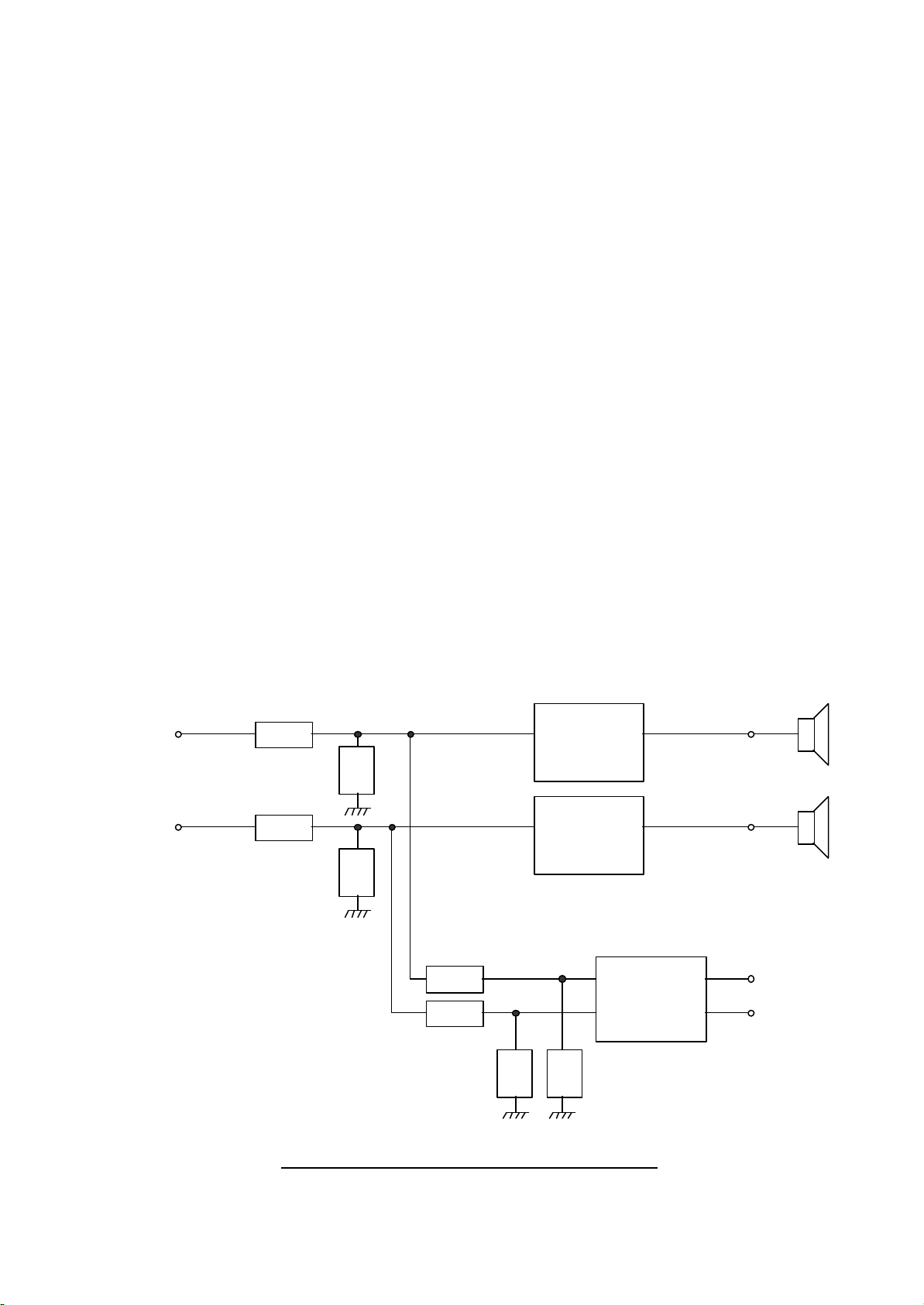
AUDIO OUTPUT
Class-D
R466
R473
R479
Class-D
Front L
R459
R468
R461
Front L
Front R
R480
R474
Head Phone
To Head
Front R
(PSA1 pin2)
The left and right signals are output from pins 1 and 2 of the PSA1 connector and are then
applied to audio amplifier I402(TDA7482) and I403(TDA7482) via the attenuation networks
R459 / R461 & R466 / R468.
The left and right output stage consists of two TDA7482 which are Class-D amplifier which
in this case is driven to give 15W per channel @ 10% thd. The power output is limited by
the Vcc supply to pin 13.
The TDA7482 has mute control line on pin 10. This control input is high when the outputs
are active and low when muted.
Headphone
The left and right signals are output from pins 1 and 2 of the PSA1 connector and are then applied
to Headphone amplifier I404(TDA2822N) via the attenuation networks R473 /R474 & R479 / R480
The TDA2822N has dual low-voltage power amplifier.
(PSA1 pin1 )
I402
Amp.
TDA7482
Amp.
TDA7482
I403
I404
Amp
TDA2822N
Speaker
Speaker
Phone
Fig.3 Sound output circuit Diagram
Page 10
Auto Digital Convergence (MAGIC FOCUS) System
1M BITS
64K BITS
8 BIT BUS
10 BIT DATA
8000 GATES
ARRAY
The auto digital convergence system can readjust convergence with one touch operation.
The system is composed of 8 photo detectors, an A/D converter, and an optical pattern
generator internal GATE ARRAY compared with conventional systems.(As shown in follow Fig.)
The System can measure the dislocation of the image in each overscanned area,
where 8 photo detectors are located, with respect to another. Therefore ,it can recover
the “good” convergence state to which the TV was adjusted , before the misconvergence occurred.
This set has three mode Digital convergence data. (PAL , NTSC Progressive, PAL 100Hz Interlace)
So need to operate three times Adjustment and setting.
PUSH SWITCH
CPU
REMOTE
CONTROLLER
EEPROM
A/D
PHOTO
DETECTOR
SCREEN
fc=16MHz
ADDRESS
PLL
H
SYNC
V
COUNTER
GATE
Fig. 8 Auto Digital Convergence System.
RAM
CORRECTION
PATTERN
ADJUSTMENT POINT 13(H x9(H)POINTS
NORMAL PATTERN
GENERATOR
OPTIONAL PATTERN
GENERATOR
AVERAGECALCULATOR
DATA CONVERTER
D/A
S/H
S/H
S/H
S/H
S/H
S/H
RV
RH
GV
GH
BV
BH
RGB
VIDEO
OUTPUT
CONVERGENCE
OUTPUT
Page 11
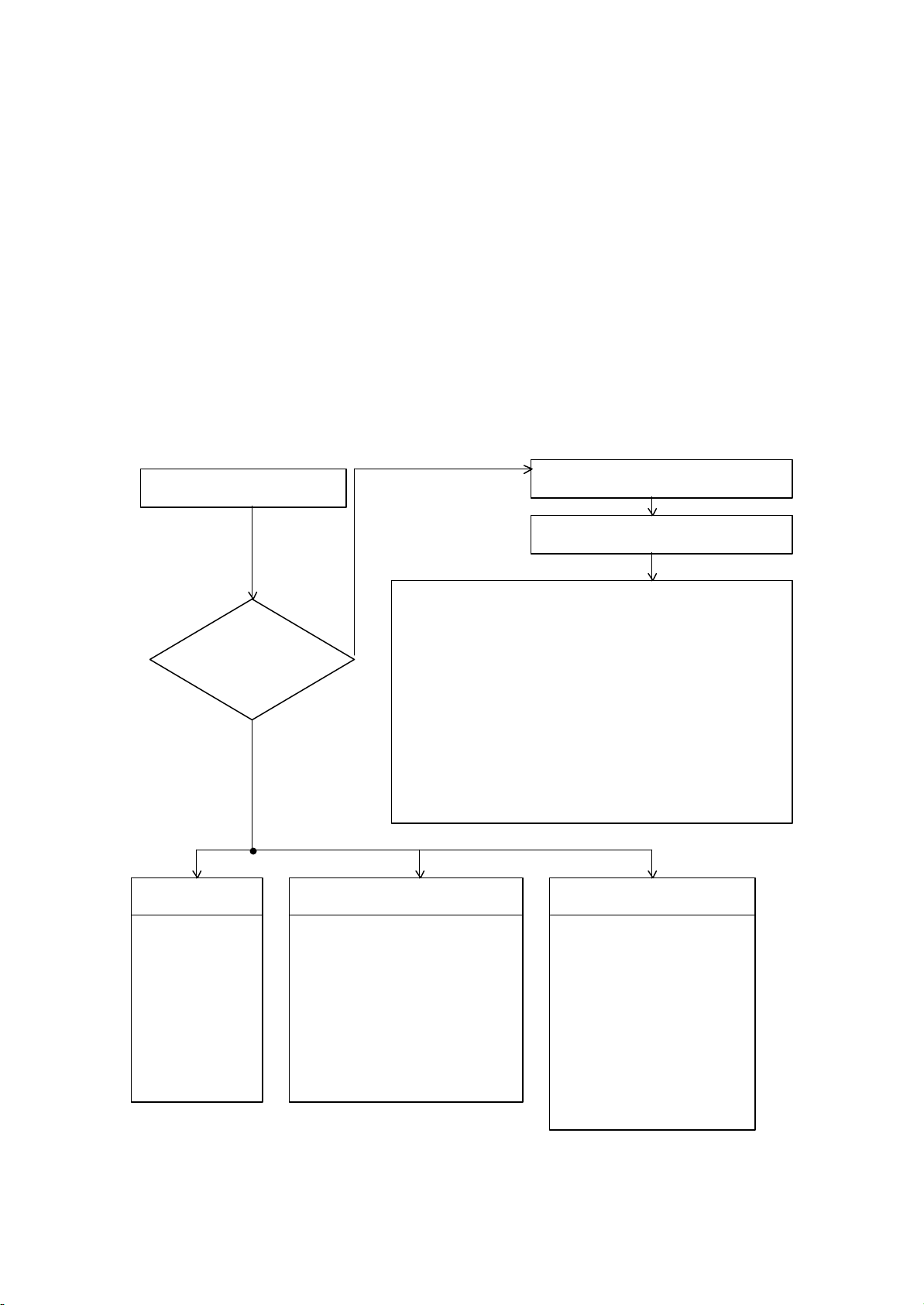
Auto Digital Convergence (MAGIC FOCUS) System
code 2,3,9 ?
Convergence Errors
Operate Initialize.
Check the error display.
Error code:1
Error code:4,5,7
Error code:10,11*
Input strong field strength
Check the wiring of
connector between sensor
No
*4
*3
*2
Yes
Convergence errors
If an error message or code appears while performing MAGIC FOCUS or INITIALIZE,
([MUTE],[LANG] while Digital convergence mode ),follow this confirmation and repair method.
1. Turn on power and input any PAL/NTSC signal.
2. Press service switch on Deflection board.
3. Press [16:9] , then [LANG] on remote control.
4. Error code will be displayed in bottom right corner of screen. If there is no error,
an “initial OK“ message will appear on screen.
5. Follow repair chart for errors.
is error
1. Darken outside light.
2. Check the sensor position No’**.
(Placement, connection and soldering)
3. Check the connector of sensor position NO**’.
4. Is pattern hitting sensor position No’**?
5. Adjustment check.(H/V size , centering)
6. Replace sensor position No’**.
7. Replace sensor PWB or DCU.
Replace DCU.
1. Check the placement of sensor.
2. Adjustment check.
(H/V size, centering)
3. Conv. amp gain check *1.
1.
signal.
2. Input standard NTSC signal.
3.
and DCU.
Page 12
Note : Error code 6 and 8 are not used .
position No.
Sensor position No.(viewed from front side)
*1 Check RK42,46,50,54,58,62 resistors first.
*2 Procedure is shown below :
Press [MUTE], then [LANG]Key.
Initialization process is now in process.
Several windows will appear and error will be displayed.
*3 Example of error display:
CONNECT 1 !
No.__
OVERFLOW!
No.__
Sensor
0 21
7
6 45
3
Page 13
DEFLECTION
Block Diagram of UP91 Deflection Circuit.
T
he operation of UP91 Deflection Circuit is as shown below.
From SIGNAL P.W.B.
VERTICAL HORIZONTAL
SYNC SYNC
VERTICAL
DRIVE DEFLECTION
CONTROL
I702
VERTICAL HORIZONTAL VERTICAL
OUTPUT DRIVE PARABOLA 1
I601 Q751
DY
VERTICAL COIL OUTPUT SIDE PIN
HORIZONTAL COIL Q777 I651, Q655, Q656, Q657
VERTICAL DYNAMIC FOCUS HI-VOLTAGE
PARABOLA 2 QF02, QF03, QF04 CONTROL
OUTPUT
FOCUS PACK
HORIZONTAL HORIZONTAL SIZE
HOT PULSE GENERATOR
QF05, QF06 IH02
QF09, QF07 HI-VOLTAGE HI-VOLTAGE
OUTPUT STABILITY
QH01 QH04, QH05
T752 IH01
HF01
FBT HI-VOLTAGE
CRT TH01 ADJUSTMENT
(R), (G), (B)
Fig. 4 Deflection Circuit Block Diagram
RH44
Page 14
SYNC Signal Processor - uPC1885A
Vertical Deflection & Geometry Controls.
The drive circuit for the vertical and E-W deflection circuits are generated by means of a
vertical divider which gets its clock from the line oscillator. The divider is synchronised
by the incoming vertical pulse, generated by the input processor or the feature box.
The vertical drive circuit outputs vertical sawtooth wave whose amplitude is set by
internal VCA circuit and on which S and C shaped correction wave are superimposed.
Center voltage of vertical sawtooth wave is changed by vertical position DAC. The
outputs must be DC coupled to the vertical output stage. The vertical geometry can be
a
djusted by I2C control via the service menu.
Horizontal Synchronisation & Drive Circuit.
The horizontal drive signal is obtained from an internal VCO which is running at a
frequency of 500KHz. The internal VCO is synchronised to the incoming H.SYNC pulse
by means of a PLL with an internal time constant. The horizontal drive signal generated
by means of a control loop which compares the phase of the reference signal from the
ternal VCO with the flyblack pulse. The time constant loop is internal.
in
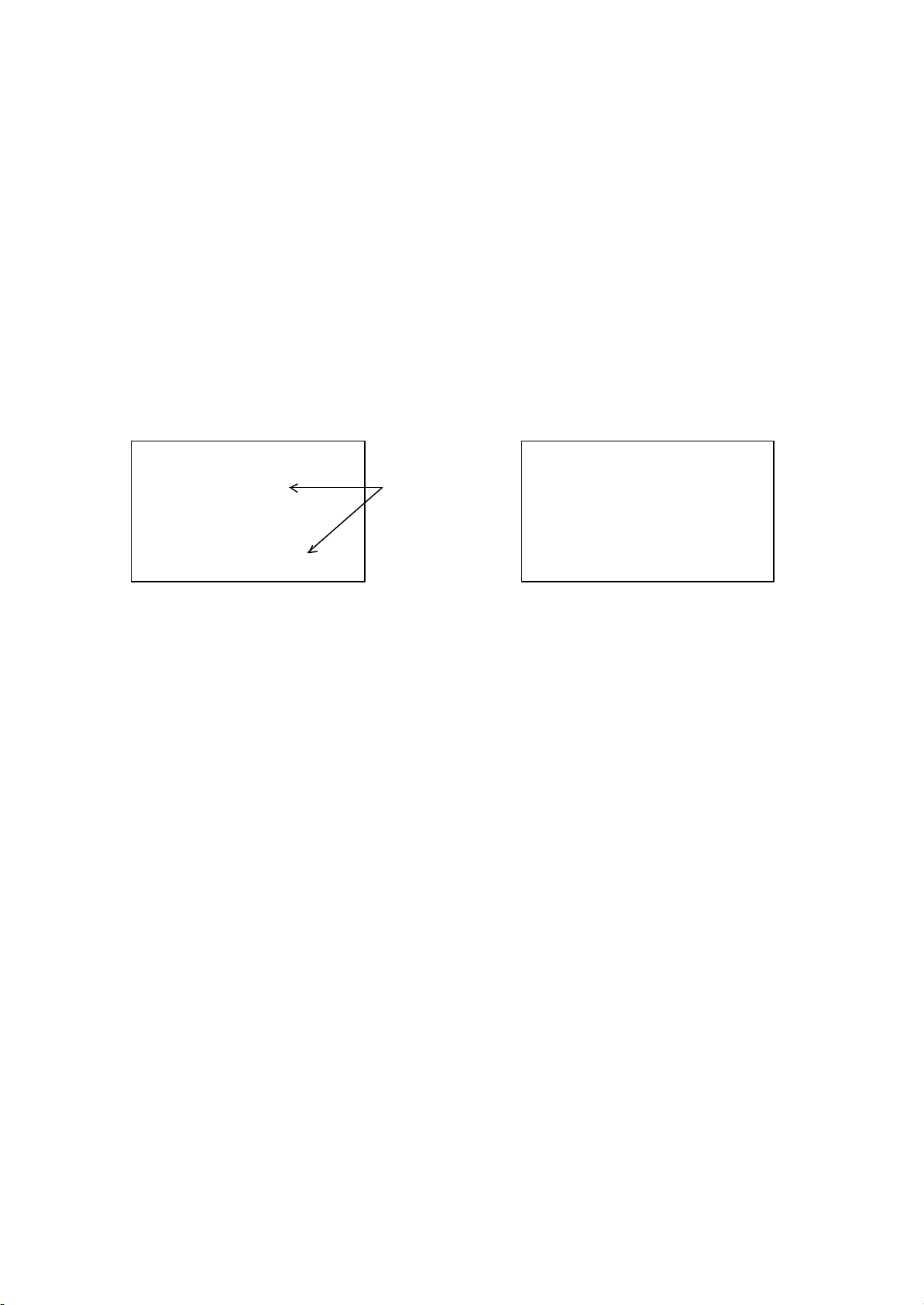
Vertical Amplifier – LA7841L
The LA7841L is vertical deflection output amplifier.
Pin 5, vertical sawtooth wave is taken with DC from pin 8 of uPC1885A.
Pin 2 outputs the vertical output voltage, and pin 7 outputs the vertical blanking pulse.
lock Diagram of LA7841 is as shown below.
B
PROTECTION
+
1 2 3 4 5 6 7
THERMAL PUMP UP
-
AMP
Fig. 5 Block Diagram of LA7841L
Page 15
Dynamic Focus
The operation of the Dynamic Focus circuit is as shown below.
Vcp
1200Vp-p
2H
C.PULSE DF07 DF08
RF35 CF18 RF15 RF21
RF14 RF22 RF25
CF11
V.PARABOLA
RF13 DF15
QF09
QF05 QF07
+12V
RF08 CF12
CF05 RF16 RF23
RF12 CF06 RF24
CF09
QF03
H. PARABOLA QF04 RF19
RF17 CF10
RF26
DF
RF10 RF11 CF08 RF18 4 1
CPT SCREEN CPT FOCUS
A
B
1V or 2V A:1000 - 1300Vp
B: 450 - 650Vp FOCUS PACK HF01
R G B R G B
Fig. 6 Dynamic Focus Circuit
The Vertical Parabola (QF09) and Horizontal Parabola (QF07) are sent to the FOCUS
PACK and Applied to the DC Focus voltage that is adjusted by the Focus Control.
These voltages are then applied to the RED, GREEN and BLUE Focus Electrodes of the
Picture Tubes in the form of a Dynamic Voltage.
Page 16
H.Linearity
The H.Linearity Circuit uses two linearity coils (L752:G,B common and L753:R).
he circuit is as shown below.
T
+
+
G H.DY
-
+
-
C765 C766
L
R759 R760
752 L753
B H.DY
R H.DY
C
TO S CURVE COLLECTOR PULSE
CORRECTION
APACITOR (C762, C763)
Fig. 7 H.Linearity Circuit
Page 17

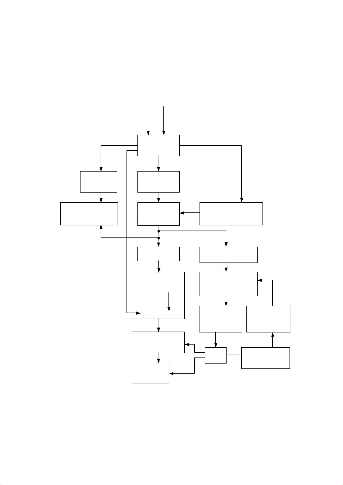
MicroController Section on the UP91 Chassis
The main m icr ocontr oller on the UP91 chas s is is loc ated at I001 (ST92R195B). This is an 80-pin QFP (quad-flat package)
that is surface m ounted for compactness. This highly com plex device controls many of the other integrated circuits via
dedicated input/output lines or the I
menus and the teletext. The device c an acquire, decode and display the teletext without the need for a separate IC. This
microcontroller is ROM-less which results in the need of a separate memor y device to store the program code nec essary
for operating the television. This m emory device is located at I002 and is multi-time program m able (MT P). T his allows the
device to be re-programmed and in the future can even be re-programmed in the board without having to remove the back
cabinet of the T V. The television s tores all the necessary customer preferences and oper ating settings in an on-board
EEPROM (E2). This device can hold 2Kb of information for storing the programme information (frequency, name, AV
setting, etc.), factory alignment settings (geometry, white balance, tuner AFC/AGC, etc.), service diagnostic errors and
customer contro l settings ( volume, br ightness, contras t, etc.). T his device com m unic ates with the m ain m ic rocontr oller via
2
the I
C bus, even in the standby mode.
Main MicroController (I001)
The ST92R195B is an enhanced microc ontroller based on the ST 9+ instruc tion set fr om ST Microelectr onics. It is c apable
2
C bus. This device also generates the RG B signals for the on-screen display (OSD)
of displaying menus and teletext for 50Hz and 100Hz televisions. This device can acquire/decode and display pages of
teletext information in FLO F (FastText) and TOP (only in Germany/Switzerland/Austria) modes. The device operates f rom
a single 4MHz crystal and a +5V supply. Dedicated address/data lines enable it to acc ess 4Mbytes of addres s space, even
though in this television it is accessing 256Kbytes (2Mbit). These address/data lines are connected to the EPROM/MTP
device which holds the instructions necessary for controlling the television.
External Memory Interface MMU Address Lines
Pins 1 (MMU0), 15 (MMU1) and 16 (MMU2) are used to access addresses above 64Kbytes. Normally pins 15 and 16 are
not used when using a 256Kbyte EPROM/MTP device (AT49F002T) in position I002.
Pin 2 (MMU3) is used to select between either the EPROM/MTP in position I002, or a future device that can be fitted in
position I003. When this line is low, the AT49F002T device in position I002 is enabled (chip enable).
Pin 17 (MMU4) is used as an output port to derive a clock signal needed for shifting the data into the 74HC595 shift
register (I006).
Pin 18 (MMU5) is not used.
External Memory Interface Control Lines
Pin 4 is the Data strobe line which is connected to the output enable input of the EPROM/MT P (I002). W hen data is read
from the EPROM/MTP, this line is temporarily low.
Pin 8 is the Read/Write line for I003. Normally, this line is not used (HIGH) but if an SRAM were to be fitted into this
position, the line could be low when writing data to the SRAM.
External Memory Interface Address Lines
Pins 3, 5, 6, 7, 13, 14 and 71 to 80 are the address lines needed to specify which location in a 256Kbyte page is needed to
Page 18

be accessed from the EPROM/MTP (I002). These lines are also connec ted to I003 if an SRAM is to be f itted in future.
Normally these lines will be changing state (0V to approx. +5V). By placing an oscilloscope on pin 12 of the EPROM/MTP
(I002) it can be confirm ed that the microcontroller is operating successf ully. In this case, this line s hould be c hanging state
very frequently.
External Memory Interface Data Lines
Pins 63 to 70 are the 8 data lines needed for receiving data from the EPROM/MT P (I002) . If an SRAM were to be fitted in
position I003, then these lines would be used to transfer data from the microcontroller to the SRAM. Under normal
circumstances these lines change from LOW (0V) to HIGH (approx. +5V).
Ground Connections
Pin 9 (GNDM) is the ground connection (0V) f or the external memory interface. This should be free of noise to enable
successful communications between the microcontroller and the EPROM/MTP (or SRAM).
Pin 35 (GND) is the digital ground connection (0V) for normal operation of the device.
Pin 62 (GNDA) is the analogue ground connection for the DAC and phase lock loops (PLL’s).
Supply Connections
Pin 10 (VDDM) is the +5V supply for the external memory interface. Without this supply, the microcontroller cannot
communicate with the EPROM/MTP (or SRAM).
Pin 34 (VDD) is the main digital supply voltage to the IC (5V 10% tolerance).
Pin 52 (VDDA) is the analogue supply voltage for the DAC’s and PLL’s (+5V). These connections ar e all jo ined together to
the +5V standby rail of the television, ensuring that the microcontroller operates even in the standby state.
Crystal Oscillator Connections
Pin 11 is the 4MHz crystal oscillator input (OSCIN).
Pin 12 is the 4MHz crystal oscillator output (OSCOUT). By connecting a x100 scope probe to pin 11, it can be seen if a
4MHz sine wave is present at the oscillator input to the microcontroller.
Reset Connection
Pin 54 is the active low RESET input of the microcontroller. This input is normally high (approx. +5V) under operating
conditions, but changes state when the standby +5V power supply is typically below +4.5V. In this circum stance, the r eset
IC (I011) pulls pin 54 low until the input of it is above +4.5V. The diode (D005) ensures that the capacitor (C024)
discharges quickly when the standby supply falls, so that the reset operates quickly. The capacitor (C024) charges up
slowly when the standby +5V supply is restored, ensuring that there is some hysteresis.
Infra-red (IR) Receiver Input
Pin 25 is the IR receiver’s filtered output. This input from the IR receiver consists of PW M pulses between 0V and +5V
which are decoded by the microcontroller into useful commands from the handset. W hen a valid command has been
decoded, the Red LED on the front of the TV will briefly flash.
Page 19

Horizontal and Vertical Synchronisation Connections
Pin 48 is the vertical synchronisation input from the deflection stage. This input is used to ensure that the OSD is displayed
in a stable vertical position. When the TV is in the standby state, this input is normally low. The vertical input is triggered on
the rising edge (positive polarity).
Pin 49 is the horizontal synchronisation input from the deflection stage. This input ensures that the OSD is displayed in
stable horizontal position. When the TV is in the s tandby state, this input is norm ally low. This input is rising edge triggere d
(positive polarity).
General Input Connections
Headphone Input
Pin 19 is used to detect if the headphone has been inserted into its s ocket. T his input is norm ally HIGH (+5V) unless the
headphone has been inserted, in which case it is near 0V. When the headphone is inserted, the headphone mode option
is then available in the "Sound Mode" Menu and the loudspeakers (and internal sub- woofer if available) in the television
are muted.
Front Panel Buttons and SAV4 Socket Inputs
Pins 36 and 38 are 2 of the 4 ADC inputs of the microcontroller.
Pin 36 is connected to the Volum e +/- buttons and the SAV4 (Hi-8) socket on the f ront panel of the TV. When the voltage
on this pin is changed to a value in a certain window, the microcontroller will interpret it as either a volume +, volume -,
volume +/- command and/or an SVHS Hi-8 connector was inserted into the Hi-8 socket.
Pin 38 is connected to the Programm e +/- and Menu buttons on the front panel of the T V. When the voltage on this pin is
changed to a value in a certain window, the microcontroller will interpret it as either a program me change or the menu
button was pressed.
General Output Connections
74HC595 Shift Register Outputs
Storage-Register Clock Output (RCLK)
Pin 20 of the microcontro ller is c onnected to the rising edge ( positive trigger ed) input (pin 12) of I006. T his line is norm all y
low when not communicating with the device or when shifting data into it. Once the f ull 8-bits have been shifted in, the
RCLK line rises in order to latch the data to the device’s outputs.
Shift-Register Clock Output (SCLK)
Pin 17 of the microcontroller (MMU4) is us ed to transf er the data into to the 8-stage shift- register on the ris ing edge of the
SCLK. 8 clock pulses are needed to transfer 8 bits of data into the shift register.
Shift-Register Data Output (SI)
Pin 21 of the microcontroller is used as the data line input to pin 14 of the shift regist er. When this line is HIGH, and the
SCLK changes from low to high, the fir s t bit of data (logical 1) is s hifted into the r egist er. When this input is low, the first bit
of data is ‘0’, on the rising edge of the SCLK.
Page 20

EEPROM Write Enable Output
Pin 22 is the E2 write enable output line, which is connected to pin 7 of the EEPROM (E2). When this output is HIGH
(approx. +5V), the E2 cannot be written to (write disable) but data from the device can be read. W hen this output is low
(0V), then data can be written to the E2. This hardware line helps to protec t the E2 from inadvertent write operations,
which could occur under abnormal circumstances.
On/Off Output
Pin 28 is the On/Off line which turns On (LOW) /Off (HIGH) the secondary supplies (+B, +37V audio rail, +8V and +5V).
The standby +12V rails are unaffected when this output is HIGH (TV in the standby state). Under normal operating
conditions, this output will be low when the TV is NOT in the standby condition.
I2C Disable Output
Pin 33 is the I2C disable output which prevents the main chassis I2C bus from being connected to the I2C bus of the
microcontroller (I001) and E2 (I002). This line is normally HIGH when the TV is in the standby state. This output is
inverted using the 74HC04 hex inverter IC (I004) and in connec ted to pins 5 and 6 of I007. In the standby condition, pins 5
and 6 of I007 (74HC4066) are low and the M.SDA and M.SCL (microcontroller) lines are disconnected f rom the SDA and
SCL (main chassis) I
writing of the data has occurred (e.g. to log fault diagnostics when the TV fails to power-up and the main chassis I
low).
2
C lines. When writing to the E2, the I2C disable output is also pulled high, to ensure that succes sful
2
C bus is
Scart Disable Output
Pin 39 is used to disable the RS232 transmit and r eceive lines from pins 10 (Rx) and 12(T x) of scart socket 2. T his is
necessary when the TV is functioning normally. However, when the TV is in s ervice or diagnose modes, then this output
will be low to enable connection of the RS232 lines of the microcontroller to the scart socket.
Mute Output
Pin 40 is the mute output for the sound signal,(e.g. TV and Monitor out). This output is HIGH when the sound signals are
in the mute condition (e.g. program up / down).
Red LED Output
Pin 42 is the red LED output, which is used to indicate the standby state and when an IR command has been successf ully
received and decoded. When the T V is in the standby state, this output will be HIGH to ensure that the red LED is br ightly
lit. When the T V is not in standby, then this output will be low, but the red LED will remain dim ly lit through resistor R081.
When an IR command has been successfully received, then the LED will flash brief ly, to inform the user that the button on
the handset was pressed correctly.
I2C Connections
Pin 23 is the I2C bus data input/output for transferring data between other I2C peripherals/devices. This line is only
connected to the EEPROM (I005) when in the standby state or when writing to the EEPROM. This line is constantly active
Page 21

when the TV is powered up and normally changes state between (+5V and 0V).
Pin 24 is the I
from the main chassis when in the standby state or when writing to the EEPROM. This line oscillates at a frequency
2
C bus clock output for cloc king the data to other I2C peripherals/devices. The c lock line is also isconnec ted
around 90KHz
RS232 Connections
Pin 30 is the RS232 Transmit line from the microcontroller. When the Scart disable output from the microcontroller (pin 39)
is low, then the TXD can be routed from pin 1 to pin 2 of I007 (74HC4066). There is never a situation whereby both disable
outputs are low.
Pin 37 is the RS232 Receive line for the microcontroller. When the Scar t disable line is low, then the data can be routed
from pin 10 of sc art 2 to pin 10 of I007 and then through to pin 37 of the m icrocontroller. There is never a situation when
both RS232 enable lines are HIGH (disable outputs LOW).
RGB Connections
Pin 44 is the OSD/Teletext RGB blanking signal necessary for allowing insertion of the OSD/Teletext onto the picture.
When this output is high (approx. +5v), then the RGB signal will be superimposed onto the current picture.
Pin 45 is the OSD blue signal necessary for displaying BLUE colours for the OSD and Teletext.
Pin 46 is the OSD green signal necessary for displaying GREEN colours for the OSD and Teletext.
Pin 47 is the OSD red signal necessary for displaying RED colours for the OSD and Teletext.
CVBS Connections
Pin 60 is the Composite Video signal input for VPS and WSS slicing. It is norm ally AC coupled and internally clamped to
ensure reliable operation. VPS (video programming system) is necessary when auto-sorting programmes in
Germany/Austria/Switzerland. WSS (wide-screen signalling) is used to indicate the aspect ratio of the incoming signal.
The TV can then use this information to display the picture in the correct format.
Pin 61 is the Composite Video signal input for Teletext acquisition and dec oding and also for sync extraction, necessary
for obtaining the correct line timings for slicing the teletext information and VPS/WSS information.
Y2-Y3-SW Output
Pin 26 is the Y2-Y3-SW relay S3(Low) or S2(High) control.
V-MUTE1 Output
Pin 29 is the V-MUTE1 output relay MUTE(High) or Active(Low) control.
Digicon-busy Input
Pin 31 is the Digicon-busy input from the Digital-Conv-Unit.
This input is used to detect if the MAGIC-FOCUS has been moved.
CUT-OFF Output
Pin 32 is used the CUT-OFF relay enable(High) or disable(Low) control.
Page 22

This output is high output is high when a PTV is indicated to Horizontal center axis.
HBLK-PH Output
Pin 41 is used to adjust the phase of the horizontal blanking .
EPROM/MTP (I002)
The device located in position I002 is used to store the program code needed by the microcontroller to operate the
television correctly. This 32 pin device is an MTP (multi-time programmable memory) which allows for it to be
re-programm ed out of the c hass is without having to erase it using conventional UV EPROM eras ers. T he devic e cur rently
used on the UP91 chassis is the AT49F002T, which can hold 256Kbytes of information (2Mbit) . T his devic e als o holds any
initialisation data to be downloaded to an EEPROM. When a blank EEPROM is fitted, the initialisation data is automatically
downloaded to it when power is applied to the chassis.
Supply/Ground Connections
Pins 32 and 16 are the +5V supply and ground connections respectively. The supply voltage of +5V is always present even
when the TV is in the standby state.
Address Connections
Pins 2 to 12, 23 and 25 to 29 are the 17 address lines needed to access the f ull 256Kbytes of 8-bit data inside the device.
These lines are connected direc tly with the microcontroller so that it can request data from the MTP when operating. An
oscilloscope can be used to check pin 12 of the MTP to check whether the microcontroller is running correctly and
accessing the MTP. This pin should be oscillating at a frequency of around 2MHz and is a non-periodic square waveform.
Data Connections
Pins 13 to 15 and 17 to 21 are the 8 data lines needed to transmit a byte at a time to the m icrocontroller. These outputs
are normally tri-state and are high-impedance when the output enable pin 24 of the MTP is HIGH. When the output enable
pin is low, the data from the required address will be output on these pins.
Output Enable Connection
Pin 24 is the output enable active low input used to control the logical state of the data lines. W hen this pin is HIGH, the
data lines are in the high impedance condition and no data is present on these pins. W hen the output enable input it LO W,
the data lines are active and output the addressed data, This line is connected to the data strobe output of the
microcontroller to ensure correct operation/timings.
Chip Enable Connection
Pin 22 is the chip enable active low input used to select the device. Normally, this input is low to enable the device.
However, the device can be placed in a standby state when accessing a future SRAM in position I003. The MMU3 line
from the microcontr oller is used to select either the SRAM or the MTP. W hen no SRAM is fitted, the chip enable pin is
always low.
Page 23

Miscellaneous
Pin 1 (VPP) is the programming voltage input pin (+12.75V needed) used to re-program the device when placed in a
special programmer. This pin is always tied to the +5V standby supply, to ensure that the device can never be
re-programmed inside the television chassis.
Pin 30 is not used in this device. However, it is s till connec ted to the MMU1 line f r om the microcontroller for use with larger
size MTP’s/EPROM’s. This line can be used to access a further 256Kbytes if such a device was fitted.
Pin 31 is the active-low programming enable pin that is used to re-program and erase the device. This pin is always
connected to the +5V standby supply to ensure that no inadvertent writes/erases are performed on the device.
SRAM (I003)
On future chassis, the position I003 will be used to hold an SRAM for teletext page storage and memory storage. A
128Kbyte device will most likely be situated here to allow 100 teletext pages to be acquired and s tored f or im m ediate fas t
access to them. The SRAM is connected to the microcontroller’s address and data lines, which are shared with the
EPROM/MTP in position I002.
Supply/Ground Connections
Pins 32 and 16 are the +5V supply and ground connections respectively. This device always has +5V connected to it, even
when the TV is in the standby state.
Address Line Connections
Pins 2 to 12, 23, 31 and 25 to 28 are the address lines needed to access the 128Kbyte of data by the microcontroller.
Data Line Connections
Pins 13 to 15 and 17 to 21 are the 8-bit data lines needed to receive/transmit a byte of data at a time to/from the
microcontroller.
Chip Enable Connections
Pins 22 and 30 are 2 chip enable inputs that need to be LOW and HIGH r es pectively for the 128Kbyte device to operate. If
either pin 22 is HIGH or pin 30 is LOW, then the device enters a standby state whereby its power consumption is
dramatically reduced (10uW). The MMU3 output pin from the m icrocontr oller (pin 2) is used to s elect the SRAM when it is
HIGH. If this pin is low, then the MTP/EPROM in position I002 is selected instead.
Write Enable Connections
Pin 29 is the active-low write enable input used to enable data to be stored inside the device. This pin is connected to the
read/write line of the microcontroller for synchronisation purposes.
74HC04 Hex Inverter (I004)
The 14-pin IC in position I004 is a high speed CMOS hex inver ter used to inver t digital signals. The pack age c onsists of 6
inverters, but only 4 are used in this application.
Page 24

Supply/Ground Connections
Pins 14 and 7 are the +5V and 0V supply connections respectively. This device always has +5V supplied to it, even when
the TV is in the standby state. Capacitor C042 is connected across the supply terminal for de-coupling.
Chip Enable Connection
Pin 1 is connected to the MMU3 output from the microcontroller and is used to select either the MTP or the SRAM. This
signal is inverted and output from pin 2 that is then connec ted to the active low chip enable input ( pin 22) of the SRAM. In
this way, only one chip enable line from the microcontroller needs to be used to enable the SRAM.
I2C Disable Connection
Pin 5 is the I2C disable input from pin 33 of the microcontroller. This signal is inverted and output at pin 6 to pins 5 & 6 of
the analogue switch (I007). W hen the micr ocontroller is in the reset c ondition, or when the TV is in the standby state, the
2
I
C disable line is HIGH. This signal m ust be inverted to disable the m icrocontr oller ’s I2C bus from the I2C bus of the rest
of the chassis.
Scart Disable Connection
Pin 13 is the RS232 Scart Disable input f rom pin 39 of the microcontroller. This input is inverted and output at pin 12,
which is then connected to pins 12 & 13 of the analogue switch (I007). W hen the m icrocontroller is in the reset state, or
when the TV is NOT in service/diagnose modes, the RS232 transmit/receive lines MUST be disconnected from pins 10
and 12 of scart socket 2. This line must then be inverted to prevent any connection being made.
EEPROM (I005)
The M24C32 EEPROM, or E2 as it is com monly known, is a 32Kbit (4Kbyte) device that holds non-volatile data when
power is removed from the TV. This device can hold information for 100 programmes, such as the name, frequency,
standard, AV setting, speaker language setting and teletext favorite pages. The EEPROM also holds diagnostic fault codes
used to help identify previous faults with the chassis (see separate section that deals explicitly with this). The E2 also holds
factory aligned parameters, such as the geometry, white balance, tuner AFC/AGC, model type, cathode level, etc. The E2
also holds the user’s preferential settings, such as the volume, balance, contrast, br ightness, etc. Data is written to/ read
from the device using the standard Philips I
2
C protocols.
Supply/Ground Connections
Pins 8 and 4 are the +5V supply and ground (0V) connections respectively. The EEPROM is powered from the +5V
standby rail so that it always has power to it, even when the TV is in standby.
I2C Connections
Pin 5 is the I2C Data line needed to transfer serial data between the microcontroller and itself. Data is changed when the
clock line is low and latched on the rising edge of the I
Pin 6 is the I
acknowledge bit. The I
2
C clock line needed to synchronise the I2C data transfer. 9 clock pulses are needed for the 8-bit data and an
2
C master clock originates from the microcontroller and operates at a frequency around 100KHz.
2
C clock.
Page 25

Address Connections
Pins 1 to 3 are the address lines used to select the I2C slave address of the device. On the M24C32 device, thes e lines
must be connected to ground in order to access the device properly.
Write Disable Connection
Pin 7 is the I2C write enable/disable input. When this input is HIGH (+5V), all I2C writes to the device are denied.
When the pin is pulled low by the microcontroller (pin 22 E2RD), data can be written to the device. In this manner,
inadvertent write operations can prevent the I
2
C data from being corrupted.
74HC595 Shift Register (I006)
The 74HC595 is a 16-pin high-speed CMOS 8-bit shift register used for additional output port capability on the UP91
chassis. 8-bit data is serially shifted into the device and then latched to the outputs when so desired. These outputs are not
used when the TV is in the standby state.
Supply/Ground Connections
Pins 16 and 8 are the +5V supply and 0V ground connections respectively. This device has +5V supplied to it, even when
the TV is in the standby state. Capacitor C048 is used to de-couple the supply.
MSP Reset Output Connection
Pin 5 is the MSP3410D reset line that is low when the MSP is being reset. This line is normally HIGH (+5V) when the TV is
operating correctly. When the T V is in the standby state, this line is low, as there is no +5V signal supply to pull the line up
through resistor R044.
Shift Register Clear Input (SCLR)
Pin 10 is an active low input necessary for clearing the shift register’s data on power-up.
Shift Register Clock Input (SCK)
Pin 11 is the shift register clock input necessary for clocking the data into the device. Eac h bit of data is latched into the
device, on the rising edge of the clock. This clock originates from pin 17 of the microcontroller.
Register Clock Input (RCK)
Pin 12 is the register clock input necessary for latching the data to the output pins. On the ris ing edge of this pin, all 8
latched bits are transferred to the output pins.
Output Enable Input (G)
Pin 13 is an active low input necessary for enabling the output ports. This pin is always connected to ground to enable the
outputs.
Shift Data Input
Page 26

Pin 14 is the shift data input necessary for transfer ring the 8 data bits into the device. W hen this line is HIG H, a logic al ‘1’
is latched into the device on the rising edge of SCK. W hen this line is low during the rising edge of SCK, a logical ‘0’ is
stored instead.
MASK-SW Output
Pin 1 is the MASK-SW relay 16:9-mode(High) or other-mode(Low) control.
INTER-PRO and PAL-NTSC Output
Pin 2 is the INTER-PRO relay Interlace(High) or Progressive(Low) control.
Pin 15 is the PAL-NTSC relay PAL(Low) or NTSC(High) control.
NTSC
60P
Pin 2 (INTER-PRO) Low Low High
Pin 15 (PAL-NTSC) High Low Low
50P 100I
PAL
C , R and F-SP-OFF Output
Pin 3 is the Center amplifier control. This output is High when the Center amplifier is in the mute condition.
Pin 4 is the Rear amplifier control. This output is High when the Rear amplifier is in the mute condition.
Pin 7 is the Front amplifier control. This output is High when the Front amplifier is in the mute condition.
P.BLK Output
Pin 15 is the P.BLK relay picture-blanking(High) or active(Low) control.
74HC4066 Analogue Switch (I007)
The 74HC4066 is a 14-pin high speed CMOS quad bilateral switch. It is used primarily for connecting/disconnecting
signals when out of/in the standby state.
Supply/Ground Connections
Pins 14 and 7 are the +5V supply and 0V ground connections respectively. This device is always powered up, even when
then television is in the standby state. Capacitor C043 ensures that the supplies are properly de-coupled.
TXD Connections
Pin 1 is the RS232 Transmit line from the microcontroller (pin 30) which is routed through to pin 2 of I007 when pin13 is
HIGH. Under normal operating conditions (and when the TV is NOT in service or diagnos e modes ), pin 1 is disc onnected
from pin 2 (and pin 12 of scart2). When the TV is in service mode, a PC can be connected to scart 2 to perform diagnostic
functions on the chassis (see separate section on diagnostic protocols for more information).
RXD Connections
Pin 11 is the RS232 receive line from the m icroc ontroller ( pin 37) which is routed through to pin 10 when pin 12 is HIGH.
Page 27

Under normal operating conditions (and when the TV is NOT in s ervice or diagnose m odes), pin 10 is disconnec ted from
pin 12 (and pin 12 of scart2). When the TV is in service m ode, a PC can be connected to scart 2 to perf orm diagnostic
functions on the chassis (see separate section on diagnostic protocols for more information).
I2C Connections
2
C Clock Connection
I
Pin 8 is the I2C master clock input from the m icrocontroller (pin 24). When pin 6 of I007 is HIGH, this line is connected to
pin 9, which enables the microcontroller to c ommunicate with other I
when the TV is in the standby state, or when power is first applied to the chassis.
2
C devices on the chassis. Pin 6 is normally LOW
I2C Data Connection
Pin 4 is the I2C data input from the microcontroller (pin 23). W hen pin 5 of I007 is HIGH, this line is connected to pin 3,
which enables the microcontroller to c om m unicate with other I
TV is in the standby state, or when power is first applied to the chassis.
2
C devices on the chassis. Pin 5 is normally LOW when the
PCF8591 A/D and D/A Converter (I008)
The PCF8591 is a Single-chip, single-supply low power 8-bit CMOS data acquisition device with four analog inputs, one
analog output and a serial I
address, allowing the use of up to eight devices c onnected to the I
and data to and for the device are transferred serially via the two-line bi-directional I
2
C -bus interface. Three addr ess pins A0,A1 and A2 are used for programm ing the hardware
2
C -bus without additional hardware. Address, control
2
C -bus.
The functions of the device include analog input multiplexing, on-chip track and hold function,8-bit analog-to-digital
conversion and an 8-bit digital-to-analog conversion. T he maximum conversion rate is given r ate is given by the maximum
speed of the I
2
C -bus.
Supply/Ground Connections
Pins 16 and 8 are the +5V supply and 0V ground connections respectively. This device is always powered up, even when
then television is in the standby state. Capacitor C049 ensures that the supplies are properly de-coupled.
AV-3-SW Input
Pin 1 is connected to the pin 8 of the Scart3 terminal.
When this input change to High, TV set is selected to Scart3 Input.
D-SIZE Input
Pin 3 is D-SIZE input from the Digital Convergence Unit. When the Magic Focus is operated, this input is changed to High.
W-SP-OFF Output
Pin 15 is the Woofer amplifier control. This output is High when the Woofer amplifier is in the mute condition.
Page 28

RESET for MSP3410D
MSK SW
C SP OFF
R SP OFF
P.BLK
F.SP OFF
INTER/PRO
PAL/NTSC
ADD
Head Phone IN
IR IN
Power Good
Digicon busy
SAV4/V+/V- KEYS
P+/P-/MENU KEYS
V Sync IN
H Sync IN
H Sync
Y2/Y3 SW
ON/OFF
MUTE1
Cut Off
Mute
HBLK-PH
Red LED
WSS
VPS
74HC595
(I006)
AV3 SW
SAV1
D size in
SIDE PANEL
WOOFER OFF
Expanded A/D&D/A
SCL
SDA
(I008)PCF8591
Main u-con(80pin)
E2RD
M.SCL
M.SDA
TXD
RXD
I2C.DIS
SCART.DIS
CLOCK(P->S)
DATA
CLOCK
(I001)
ST92R195B
•E
•E
MMU3
E2P ROM
E2P DIS
M.SCL
M.SDA
ST24C32
(I005)
M.SCL
M.SDA
74HC4066
I2C.ENA
SCART.ENA
•B
74HC04
(I004)
OSD R
OSD G
OSD B
OSD BLK
SCL
SDA
(I007)
SCART TX
SCART RX
•E
•E
•E
•E
•E
•E
•E
•E
•E
•E
•E
•E
TUNER
SCL
SDA
UVE25-EW54D
(U101)
IF/Video Chroma/Analogue SW
SCL
SDA
(I201)
(IC02)
(U301)
TDA9320H
Digital 3 Line Comb
SCL
SDA
TC9090AN
Feature Box
SCL
SDA
SDA9206
SDA9400
SDA9280
RGB PROCESSOR
SCL
SDA
AV1 IN
AV2 IN
DSN
MMU0•`5
DAT0•`7
ADDR0•`15
ROM
AT49F002T
(I002) CXD2053AM
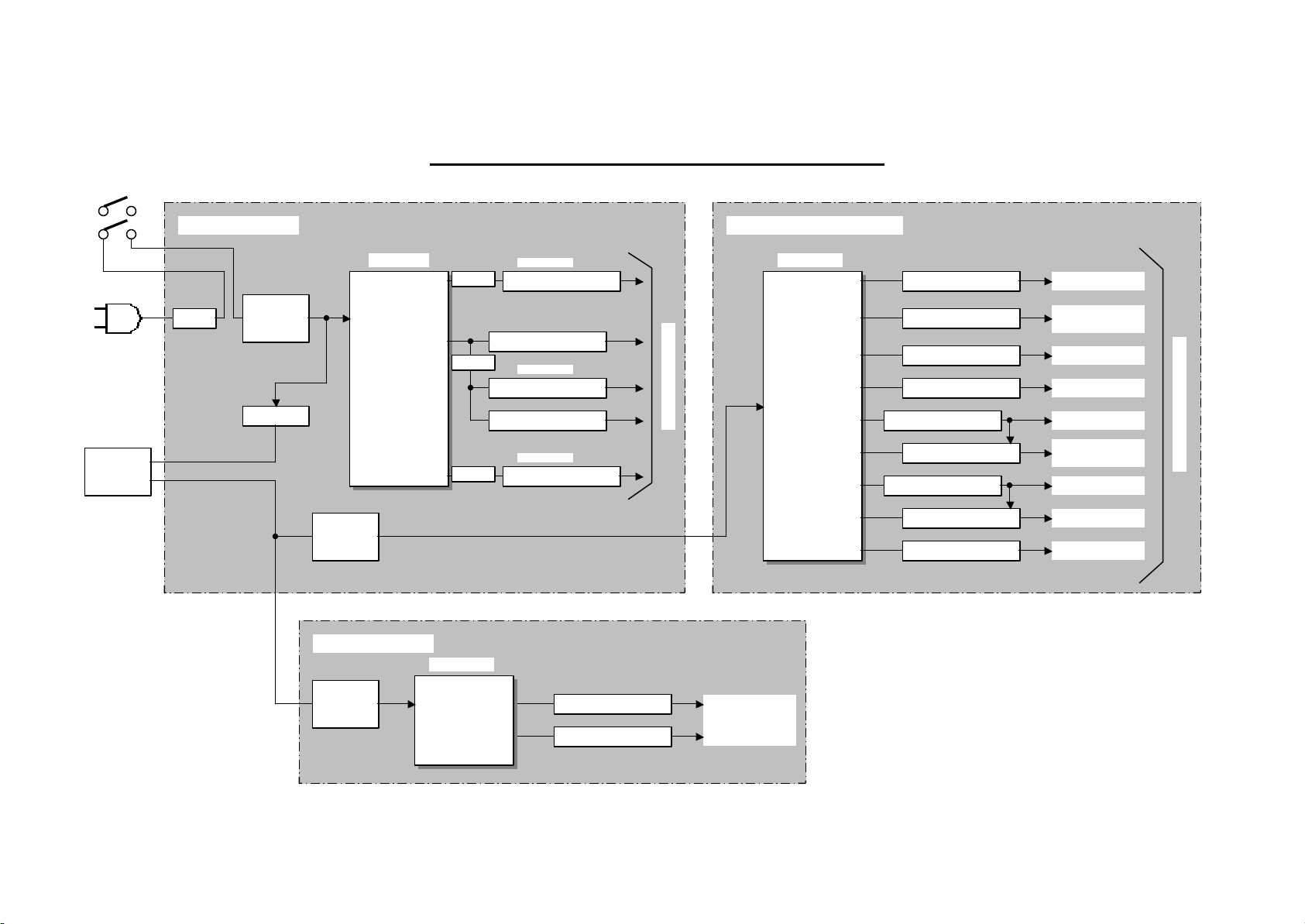
HHEE-MD DEVELOPMENT (HARD/SOFT)
AC3/MPEG DECORDER
CODEC
SUB u-con
MDSP56362
(IS01)
VOL/TONE
VOL/TONE
SCL
SDA
SCL
SDA
SCL
SDA
•E
•E
•E
•E
Fig.9 Block Diagram
MMU0•`5
ADDR0•`15
RAM
(I003)
DSN
RWN
DAT0•`7
Defrection
uPC1885
(I702)
SCL
SDA
ADD
•E
•E
•E
•E
•E
•E
(IX01)
Letter BOX Det
(I009)
(I401)
TA1276AN
SCL
SDA
A2/NICAM/SW
SCL
SDA
MSP3410D
Page 29

UP91 Signal circuit description
Tuner.
The tuner U101, is a frequency synthesis type with an unbalanced input, powered from the +5V rail while the tuning voltage is supplied by the +33V
rail, supplied from the power supply circuit. Direct frequency access, channel selection, AGC and AFC functions are controlled via the I2C bus. AGC,
AFC and Offset controls may be selected by entering the service menu and selecting the ‘tuner’ option.
Pin 1, AGC is taken from pin 62 of I201 TDA 9320. The balanced I.F. output is taken from pins 10 & 11, which are then arrive at the vision SAW filter
X209 (pins 1 & 2) and sound SAW filter X208 (pi1 B/G, D/K, L, pin2 L’). The outputs from X208 and X209 (pins 4 & 5 respectively) pass through to
pins 2 & 3 and pins 63 & 64 of I201, where they are demodulated.
Input Processor - TDA 9320(9321).
The TDA9320(9321) is a multistandard input processor. Features include:
Vision I.F. demodulation and amplifier.
The video signal is demodulated by means of a PLL carrier regenerator. This circuit contains a frequency detector and a phase detector. During
acquisition the frequency detector will tune the VCO to the right frequency. After lock-in, the phase detector controls the VCO so that a stable phase
relation between VCO and the input signal is achieved. The VCO is running at double the I.F. frequency with the reference signal for the demodulator
obtained by means of a frequency divider circuit.
The AFC output is obtained by using the VCO control voltage of the PLL and can be read via the I2C bus. The AGC detector operates on top sync and
top white level. The time constant on the AGC system during positive modulation is rather long to avoid visible variations of the signal amplitude. To
improve the speed of the AGC system a circuit has been included which detects whether the AGC detector is activated every frame period. When
during 3 field periods no action is detected the speed of the system is increased. For signals without peak white information the system switches
automatically to a gated black level AGC. Because a black level clamp pulse is required for this way of operation the circuit will only switch to black
level AGC in the internal mode.
The circuit contains a video identification circuit which is independent of the synchronisation circuit. Therefore search tuning is possible when the
display section of the receiver is used as a monitor.
Sound I.F. demodulation and amplifier.
In case of FM, NICAM, and A2 stereo, the circuit detects sound carrier signal and sends it to MSP3410 as a QSS (quasi sprit sound) carrier signal and
MSP 3410 will demodulate to base band sound.
However, in AM mode, the circuit detects AM signal and send it to MSP3410 as a base band AM signal. Then MSP3410 will provide sound to other
circuit.
Video Outputs/External Inputs
The input processor has provision for three CVBS inputs (1 internal & 2 external) and 2 Y/C inputs. The external CVBS inputs are being used for the
rear Scart sockets and front AV phono. The Y/C inputs are being used as a front S-VHS and a second, third CVBS (Scart) input. The circuit can detect
whether CVBS or a Y/C signal is present to Scart2, Scart3 and Front AV(Phono and S-VHS) inputs. The IC has 2 RGB inputs with fast switching. The
switching of the various sources is controlled by I2C and detection of a Comb filter can be made.
Page 30

Synchronisation.
The sync separator is operated by the Feature Box circuit.
Chroma & Luma Processing.
The IC contains a chrominance bandpass filter , the SECAM cloche and chrominance trap. The filters are calibrated using the tuning frequency and the
crystal frequency of the colour decoder. The luminance output signal which is derived from the incoming CVBS or Y/C signal can be varied in
amplitude by means of a separate gain control.
Colour Decoding.
The colour decoder can decode PAL, NTSC and SECAM signals. The PAL / NTSC decoder contains an alignment free crystal oscillator with 4 separate
pins, a killer circuit and two colour difference demodulators. The 90-degree phase shift for the reference signal is made internally. Because it is possible
to connect 4 different crystals to the colour decoder, all colour standards can be decoded without external switching circuits. Crystals not used must be
left open. The horizontal oscillator is calibrated by means of the crystal frequency of the PLL.
The IC contains an automatic colour limiting circuit which is switchable which prevents over saturation when signals with a high chroma-to-burst ratio
are received. The ACL circuit is designed such that it only reduces the chroma signal and not the burst. This has the advantage that the colour
sensitivity is not affected by this function.
The SECAM decoder contains an auto-calibrating PLL demodulator which has two references, the 4.43MHz sub-carrier frequency which is obtained
from the crystal oscillator which is used to tune the PLL to the desired free running frequency and the bandgap reference to obtain the correct absolute
value of the output signal. The VCO of the PLL is calibrated during each vertical blanking period, when the I.C. is in search or SECAM mode. The
base-band delay line is integrated into the package in order to adjust luminance and chrominance timing.
Signal Path Description.
The I.F. signal is obtained from SAW filters X209 (vision) and X208 (Sound) pins 4 & 5 and are fed into pins 2 & 3 vision and 63 & 64 sound of I201
respectively. A composite video signal is available at pin 10 from the vision demodulator. Either QSS carrier or AM base band sound out from pin 5.
The video is taken from pin 10 via C304 into pin 12 and out at pin 13. This is the selectable Group Delay adjustment via software input output for the
compensation of difference between I&B/G. The composite video gets taken through buffer and sound trap stages where the desired video returns to
I201 at pin 14.
The AV switching matrix supports three Scart sockets, phono (front) CVBS and S-VHS inputs. Scart CVBS inputs are at pins 20 and proceed to pin 16
(Scart1 JY01) and 20 (Scart2, JY02 or Scart3, JY03, Scart2 and Scart3 are selected by external video switch IY01 on terminal PCB, beforehand.) CVBS
outputs to Scart pins 19 from emitter of QY04 (Scart1), emitter of QY01 (Scart2) and emitter of QY03 (Scart3). Scart S-VHS inputs which are via JY02 or
JY03 (switched by IY01) to pin 20 & 21 of I201. Front S-VHS input is via din socket JM02 to pin 23 & 24 of I201. Detection of CVBS input is detected
within I201. Comb filter output has been fitted via Y/C input pins 28 & 29. Colour sub-carrier output for the Comb filter is form pin 30.
Y, U and V signals are taken from I201 pins 49, 50 & 51 and go into pins 9, 10 & 12 of the double scan unit (U301) respectively.
Other miscellaneous pins. I2C control lines are pins 46 & 47, and tuner AGC control voltage is present at pin 62. Sandcastle pin 59 is not in use. HA,
VA out from pins 60 & 61 are also not in use.
Digital Comb Filter.
The operation of a comb filter is to separate the composite video into luminance and reconstructing the chrominance sub carrier signals using digital
signal processing techniques. The comb filter IC, IC02 has an additional vertical edge enhancement feature.
Composite video input (Pin 6 of connector PN01) and colour sub-carrier (pin 8 of PN01) is to an analogue to digital 8 bit converter where the vertical
Page 31

enhancement and digital comb filtering takes place. Separated luminance and chrominance output
components are available via a digital to analogue 8 bit converter at pins 1 & 4 of PN01 respectively.
Digital Double Scan Conversion Unit (Feature Box).
The main feature of this unit is frequency double scan conversion 100Hz interlaced and 50/60Hz progressive scan.
Other features of this unit are noise reduction, line flicker reduction, CTI (Colour Transient Improvement),
sharpness, vertical zoom and horizontal compression. These functions arecontrolled by I2C bus. This unit is powered
from +5V and +8V supplies, feeding into pins 1, 2 and 6 of E U02 respectively. The three input 50Hz video
signals Y, U, V are sent to this unit at pins 8, 10 and 12 of EU01. The Y, U, V video output signals (double frequency
video) are taken from pins 5, 3 and 1 of EU01. The horizontal and vertical sync signals are input to this unit as a
composite video signal at 4 of EU02, the double frequency sync signals outputs are from pins 10 and 11of EU02.
Page 32

FIG.1 Scan rate conversion mode for display
Fig.1 shows the differences between 100Hz interlaced scan and 50/60Hz progressive scan.
The biggest advantage of progressive scan is "non-interlacing", but field frequency is kept at 50/60Hz.
This means the line construction (density) is twice, compared with 100Hz interlaced scan. Therefore, if
progressive scan mode is selected, large area flicker will be still appeared on display, but will eliminate lines flicker.
RGB Processor - TA 1276AN
The TA1276AN is RGB Processor IC which included features are Black stretch, Gamma correction,
Contrast/Brightness/Colour/Tint/Sharpness controls, G and B drive gain control and Velocity Scan Modulation
signal control. The Black stretch is stable operated at each of the viewing format, by input the Clamp pulse
signal to pin 25 of TA1276AN from the 4:3 frame generator which are consisted of IZ03 and IZ05.
Input Signals.
Y, U, V, input signals which are supplied by the feature box. The nominal input signal for Y is 0.7V Peak-to-Peak.
The nominal input signals for U and V are 300mV Peak-to-Peak respectively.
Page 33

Two RGB sources are intended for use by the Digital Convergence Adjustment Signal, while the second is
used for the OSD and Teletext. The required input signal has an amplitude of 0.5V Peak-to-Peak.
The switching between the internal signal and the OSD signal can be realized via a OSD BLK.
The circuit contains switchable matrix circuits for the colour difference signal so that the colour reproduction can
be adapted for PAL/SCAM and NTSC.
I2C is present at pins 27 & 28 (IX01) and +9V supply rails at pins 22, 40 & 46 and +5V supply rails at 12 pin.
From
Feature Box
2H Sync
Mask SW
IZ03
Clamp
74HC221
Gen.
4:3 Frame
Gen.
IZ05
74HC221
Clamp
pulse
Y
U
V
RGB Processor
Y
U
V
VM
To
CRT PCB
IX01 TA1276AN
Fig2. RGB Processor Block Diagram
CRT base
RGB signals for CRT are applied by PZC connector from RGB PCB to B CRT base PCB and bridged to G, R
CRT base PCB into Q8A1, Q851, and Q801. Then for e.g. B signal goes through limiter circuit Q8A2, Q8A3 to
amplifier Q8A4, Q8A5. B CRT base particularly has a gamma correction circuit, Q8A6 & Q8A7 which is
compensating B tube phosphorcharacteristic. Because B tube phosphor efficiency reduces in high brightness
area, therefore the B gain must be higher than others in high brightness area G CRT base has a bias circuit
Q858, Q859 for all CRT base PCB. Protection signal, which is called spot, is fed to CRT base to blank the picture
when something has failed.
Scan Velocity Modulation.
During transmission the signal sufferers from degradation and also due to the frequency characteristics of the television circuitry.
This normally results in a gentle rise or fall in the brightness change areas where black-to-white-to-black
patterns are received. The picture sharpness quality can be assessed by how steep the leading and trailing edges
are. The scan velocity modulation circuit has been designed to improve picture quality, ie make the video signal edges
steeper, by controlling the horizontal scanning velocity of the electron beam in the CRT. The velocity modulation
Page 34

circuit produces a compensation signal by differentiated luminance signal. The compensation signal is given some
current gain,applied to the auxiliary coil (connectors PVMR, PVMG, PVMB) on the neck of the cathode ray tube
(CRT) tocontrol the speed of the electron beam. The VM circuit is located beside CRT base PCB, on the backside
of lower part of front cabinet. The differentiated luminance signal derives from PZV pin 1 and into base of QE01,
through the CE03, RE04 arriving at the emitter of QE02 QE03 for voltage amplification and latter stages,
power
gain.
Page 35

SM00026 SIGNAL PCB 1 of 4
Page 36

SM00026 EUROPE PTV SIGNAL 2 of 4
Page 37

SM00026 SIGNAL PCB 3 of 4
Page 38

SM00026 EUROPE PTV SIGNAL 4 of 4
Page 39

SM00026 UP9X DEFLECTION CIRCUIT 1 of 3
Page 40

SM00026 UP9X DEFLECTION CIRCUIT 2 of 3
Page 41

SM00026 UP9X DEFLECTION CIRCUIT 3 of 3
Page 42

SM00026 UP9X SUB DEFLECTION CIRCUIT
Page 43

COMB FILTERSM00026
Page 44

SM00026
EURO PTV CONTROL - A
Page 45

EURO PTV CONTROL - BSM00026
Page 46

AUDIO AMP BOARD 1 of 2SM00026
Page 47

AUDIO AMP BOARD 2 of 2SM00026
Page 48

EUROPE PTY TERMINALSM00026
Page 49

UP9X SENSORSM00026
Page 50

UP9X RGB CIRCUITSM00026
Page 51

SM00026 UP91 POWER SUPPLY
Page 52

SM00026 AUDIO DECODER
Page 53

SM00026
HIGH END FEATURE BOX
Page 54

110W SUB POWER BOARDSM00026
Page 55

SM00026 CPT CIRCUIT
Page 56

SM00026 VM CIRCUIT
Page 57

SM00026 UP9X VM PCB
Page 58

I/V I/F PCBSM00026
Page 59

AUDIO AMPLIFIER BOARD (SOLDER)SM00026
Page 60

AUDIO AMPLIFIER BOARD (COMPONENT)SM00026
Page 61

UP9X SIGNAL (SOLDER)SM00026
Page 62

UP9X SIGNAL (COMPONENT)SM00026
Page 63

UP9X CPT-B PCBSM00026
Page 64

UP9X SENSOR PCBSM00026
Page 65

110W SUB POWER PCBSM00026
Page 66

UP9X DEFLECTION PCB (SOLDER)SM00026
Page 67

UP9X DEFLECTION PCB (COMPONENT)SM00026
Page 68

AUDIO DECODERSM00026
Page 69

HIGH END FEATURE BOX PCBSM00026
Page 70

UP9X CONTROL-A PCBSM00026
Page 71

UP9X CONTROL-B PCBSM00026
Page 72

UP9X COMB FILTERSM00026
Page 73

UP9X SUB DEFLECTION PCBSM00026
Page 74

UP9X TERMINAL PCBSM00026
Page 75

THE UPDATED PARTS LIST
FOR THIS MODEL IS
AVAILABLE ON ESTA
Page 76

Notes
Page 77

Hitachi, Ltd. Tokyo, Japan
International Sales Division
THE HITACHI ATAGO BUILDING,
No. 15 –12 Nishi Shinbashi, 2 – Chome,
Minato – Ku, Tokyo 105-8430, Japan.
Tel: 03 35022111
HITACHI EUROPE LTD,
Whitebrook Park
Lower Cookham Road
Maidenhead
Berkshire
SL6 8YA
UNITED KINGDOM
Tel: 01628 643000
Fax: 01628 643400
Email: consumer-service@hitachi-eu.com
HITACHI EUROPE GmbH
Munich Office
Dornacher Strasse 3
D-85622 Feldkirchen bei München
GERMANY
Tel: +49-89-991 80-0
Fax: +49-89-991 80-224
Hotline: +49-180-551 25 51 (12ct/min)
Email: HSE-DUS.service@hitachi-eu.com
HITACHI EUROPE srl
Via Tommaso Gulli N.39, 20147
Milano, Italia
ITALY
Tel: +39 02 487861
Tel: +39 02 38073415 Servizio Clienti
Fax: +39 02 48786381/2
Email: customerservice.italy@hitachi-eu.com
HITACHI EUROPE S.A.S
Lyon Office
B.P. 45, 69671 BRON CEDEX
FRANCE
Tel: 04 72 14 29 70
Fax: 04 72 14 29 99
Email: france.consommateur@hitachi-eu.com
HITACH EUROPE AB
Egebækgård
Egebækvej 98
DK-2850 Nærum
DENMARK
Tel: +45 43 43 6050
Fax: +45 43 60 51
Email: csgnor@hitachi-eu.com
Hitachi Europe Ltd
Bergensesteenweg 421
1600 Sint- Pieters-Leeuw
BELGIUM
Tel: +32 2 363 99 01
Fax: +32 2 363 99 00
Email: sofie.van.bom@hitachi-eu.com
www.hitachidigitalmedia.com
HITACHI EUROPE S.A.
364 Kifissias Ave. & 1, Delfon Str.
152 33 Chalandri
Athens
GREECE
Tel: 1-6837200
Fax: 1-6835964
Email: service.hellas@hitachi-eu.com
HITACHI EUROPE S.A.
Gran Via Carlos III, 101- 1
08028 Barcelona
SPAIN
Tel: 93 409 2550
Fax: 93 491 3513
Email: atencion.cliente@hitachi-eu.com
HITACHI Europe AB
Box 77 S-164 94 Kista
SWEDEN
Tel: +46 (0) 8 562 711 00
Fax: +46 (0) 8 562 711 13
Email: csgswe@hitachi-eu.com
HITACHI EUROPE LTD (Norway) AB
STRANDVEIEN 18
1366 Lysaker
NORWAY
Tel: 67 5190 30
Fax: 67 5190 32
Email: csgnor@hitachi-eu.com
HITACHI EUROPE AB
Neopoli / Niemenkatu 73
FIN-15140 Lahti
FINLAND
Tel : +358 3 8858 271
Fax: +358 3 8858 272
Email: csgnor@hitachi-eu.com
HITACHI EUROPE LTD
Na Sychrove 975/8
101 27 Praha 10 – Bohdalec
CZECH REPUBLIC
Tel: +420 267 212 383
Fax: +420 267 212 385
Email: csgnor@hitachi-eu.com
 Loading...