

Hitachi 2SK322 Schematic [ru]
Application
HF wide band amplifier
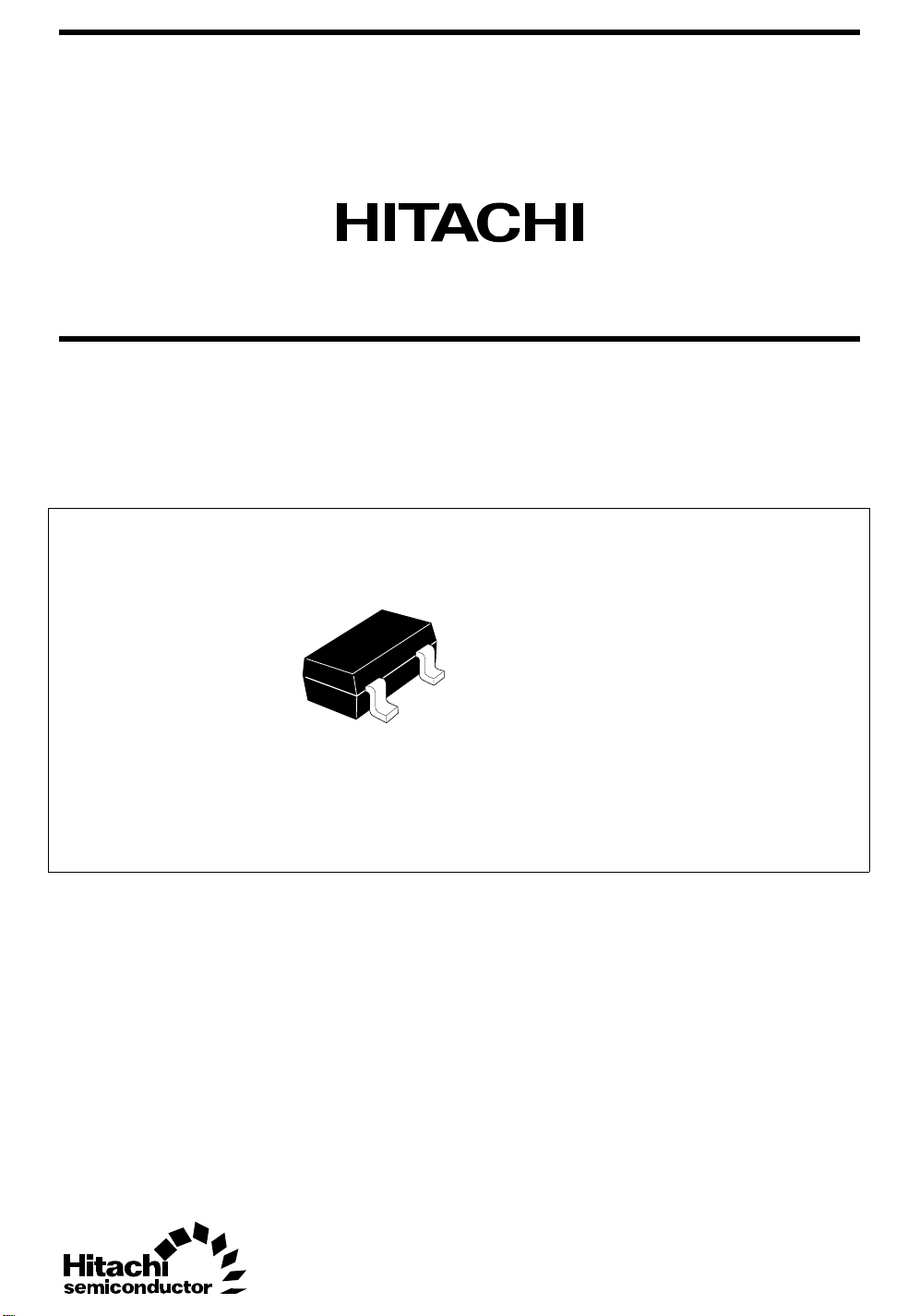
Outline
MPAK
2SK322
Silicon N-Channel Junction FET
3
1
2
1. Drain
2. Source
3. Gate

2SK322
Absolute Maximum Ratings (Ta = 25°C)
Item Symbol Ratings Unit
Gate to drain voltage V
Gate to source voltage V
Drain current I
Gate current I
GDO
GSO
D
G
Channel power dissipation Pch 150 mW
Channel temperature Tch 150 °C
Storage temperature Tstg –55 to +150 °C
Electrical Characteristics (Ta = 25°C)
Item Symbol Min Typ Max Unit Test conditions
Gate to drain breakdown
V
(BR)GDO
voltage
Gate to source breakdown
V
(BR)GSO
voltage
Gate cutoff current I
Drain current I
Gate to source cutoff voltage V
GSS
DSS
GS(off)
Forward transfer admittance |yfs| 25 45 — mS V
Note: 1. The 2SK322 is grouped by I
Grade P Q R S T
Mark WP WQ WR WS WT
I
DSS
5 to 16 14 to 24 20 to 32 28 to 42 36 to 50
–15 — — V IG = –100 µA
–15 — — V IG = –100 µA
— — –10 nA VGS = –7 V, VDS = 0
1
*
5 — 50 mA VDS = 5 V, VGS = 0 (pulse)
— — –3.0 V V
as follows.
DSS
–15 V
–15 V
50 mA
5mA
= 5 V, ID = 100 µA
DS
= 5 V, VGS = 0, f = 1 kHz
DS
2
2SK322
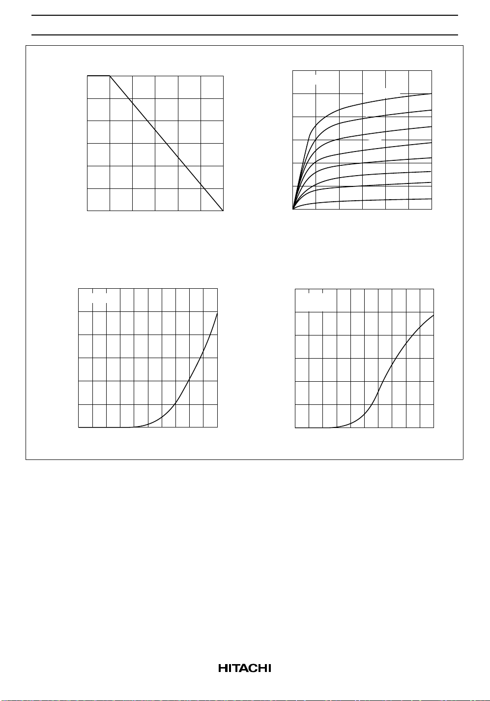
Maximum Channel Power Dissipation
Curve
150
(mW)
ch
100
50
Channel Power Dissipation P
0
Ambient Temperature Ta (°C)
Typical Transfer Characteristics
30
VDS = 5 V
20
(mA)
D
Typical Output Characteristics
30
VDS = 5 V
= 0 V
V
GS
20
(mA)
D
–0.1
–0.2
–0.3
10
Drain Current I
–0.4
–0.5
–0.6
–0.8
15010050
0
Drain to Source Voltage V
DS
642
(V)
Forward Transfer Admittance vs.
Gate to Source Voltage
60
VDS = 5 V
(mS)
f = 1 kHz
fs
50
40
30
10
Drain Current I
0
Gate to Source Voltage V
GS
(V)
20
10
Forward Transfer Admittance y
0–2.0 –1.2 –0.8 –0.4–1.6
0
Gate to Source Voltage V
GS
0–2.0 –1.2 –0.8 –0.4–1.6
(V)
3
 Loading...