

Page 1
1
2
3
查询2SK1296供应商
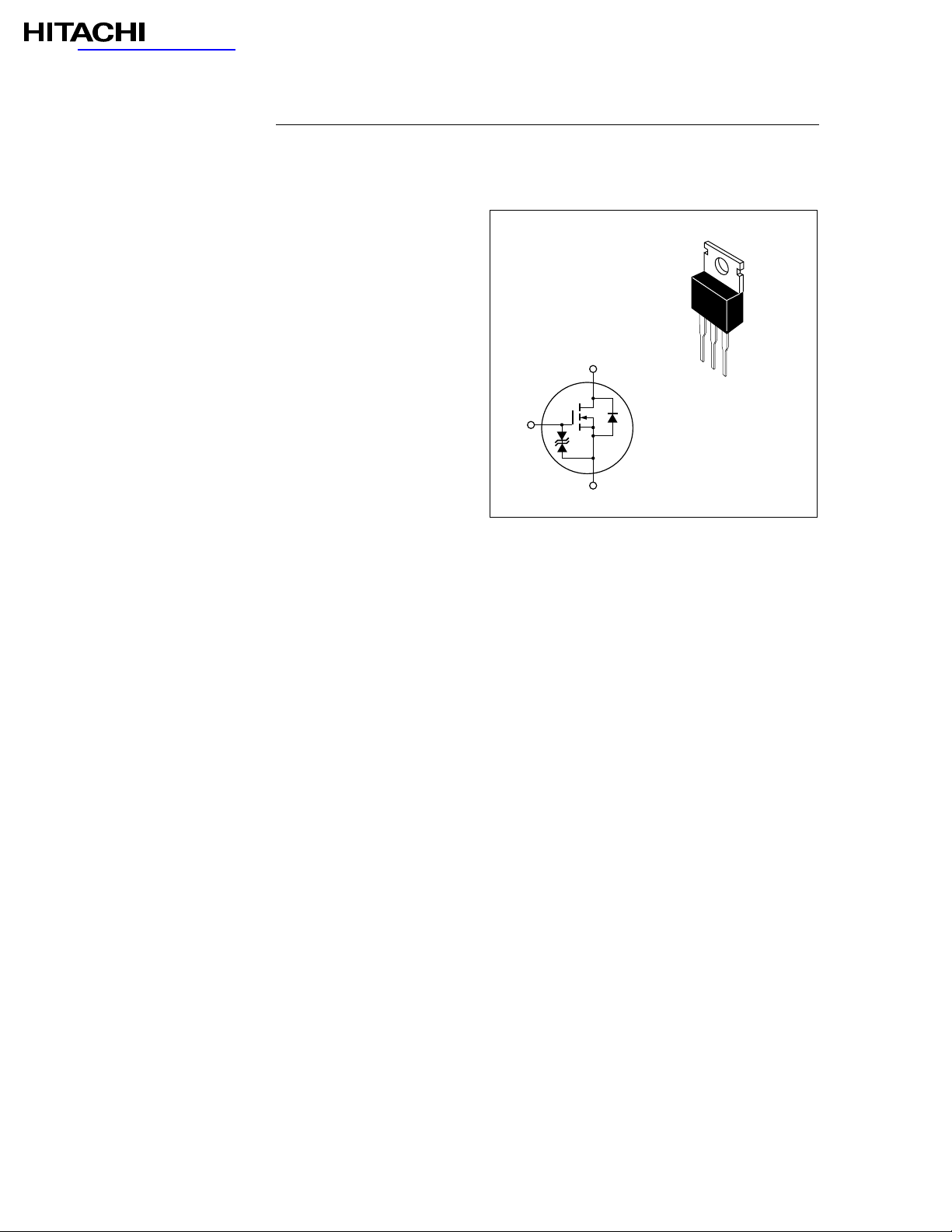
2SK1296
Silicon N-Channel MOS FET
Application
High speed power switching
Features
TO–220AB
• Low on-resistance
• High speed switching
2
• Low drive current
• 4 V gate drive device
– Can be driven from 5 V source
• Suitable for motor drive, DC-DC converter,
power switch and solenoid drive
1
3
1. Gate
2. Drain
(Flange)
3. Source
Table 1 Absolute Maximum Ratings (Ta = 25°C)
Item Symbol Ratings Unit
———————————————————————————————————————————
Drain to source voltage V
DSS
60 V
———————————————————————————————————————————
Gate to source voltage V
GSS
±20 V
———————————————————————————————————————————
Drain current I
D
30 A
———————————————————————————————————————————
Drain peak current I
D(pulse)
* 120 A
———————————————————————————————————————————
Body to drain diode reverse drain current I
DR
30 A
———————————————————————————————————————————
Channel dissipation Pch** 75 W
———————————————————————————————————————————
Channel temperature Tch 150 °C
———————————————————————————————————————————
Storage temperature Tstg –55 to +150 °C
———————————————————————————————————————————
* PW ≤ 10 µs, duty cycle ≤ 1 %
** Value at T
= 25 °C
C
Page 2

2SK1296
Table 2 Electrical Characteristics (Ta = 25°C)
Item Symbol Min Typ Max Unit Test conditions
———————————————————————————————————————————
Drain to source breakdown V
voltage
(BR)DSS
60 — — V ID= 10 mA, VGS= 0
———————————————————————————————————————————
Gate to source breakdown V
voltage
(BR)GSS
±20 — — V IG= ±100 µA, VDS= 0
———————————————————————————————————————————
Gate to source leak current I
GSS
— — ±10 µA VGS= ±16 V, VDS= 0
———————————————————————————————————————————
Zero gate voltage drain current I
DSS
— — 250 µA VDS= 50 V, VGS= 0
———————————————————————————————————————————
Gate to source cutoff voltage V
GS(off)
1.0 — 2.0 V ID= 1 mA, VDS= 10 V
———————————————————————————————————————————
Static drain to source on state R
resistance
DS(on)
— 0.024 0.028 Ω ID= 15 A, VGS= 10 V *
——————————— ——————————–
— 0.030 0.040 ID= 15 A, VGS= 4 V *
———————————————————————————————————————————
Forward transfer admittance |yfs| 1727—SI
= 15 A, VDS= 10 V *
D
———————————————————————————————————————————
Input capacitance Ciss — 2250 — pF VDS= 10 V, VGS= 0,
————————————————————————————————
Output capacitance Coss — 1230 — pF f = 1 MHz
————————————————————————————————
Reverse transfer capacitance Crss — 300 — pF
———————————————————————————————————————————
Turn-on delay time t
d(on)
— 20 — ns ID= 15 A, VGS= 10 V,
————————————————————————————————
Rise time t
r
— 125 — ns RL= 2 Ω
————————————————————————————————
Turn-off delay time t
d(off)
— 390 — ns
————————————————————————————————
Fall time t
f
— 225 — ns
———————————————————————————————————————————
Body to drain diode forward V
voltage
DF
— 1.3 — V IF= 30 A, VGS= 0
———————————————————————————————————————————
Body to drain diode reverse t
recovery time di
rr
— 160 — ns IF= 30 A, VGS= 0,
/dt = 50 A/µs
F
———————————————————————————————————————————
* Pulse Test
Page 3
2SK1296
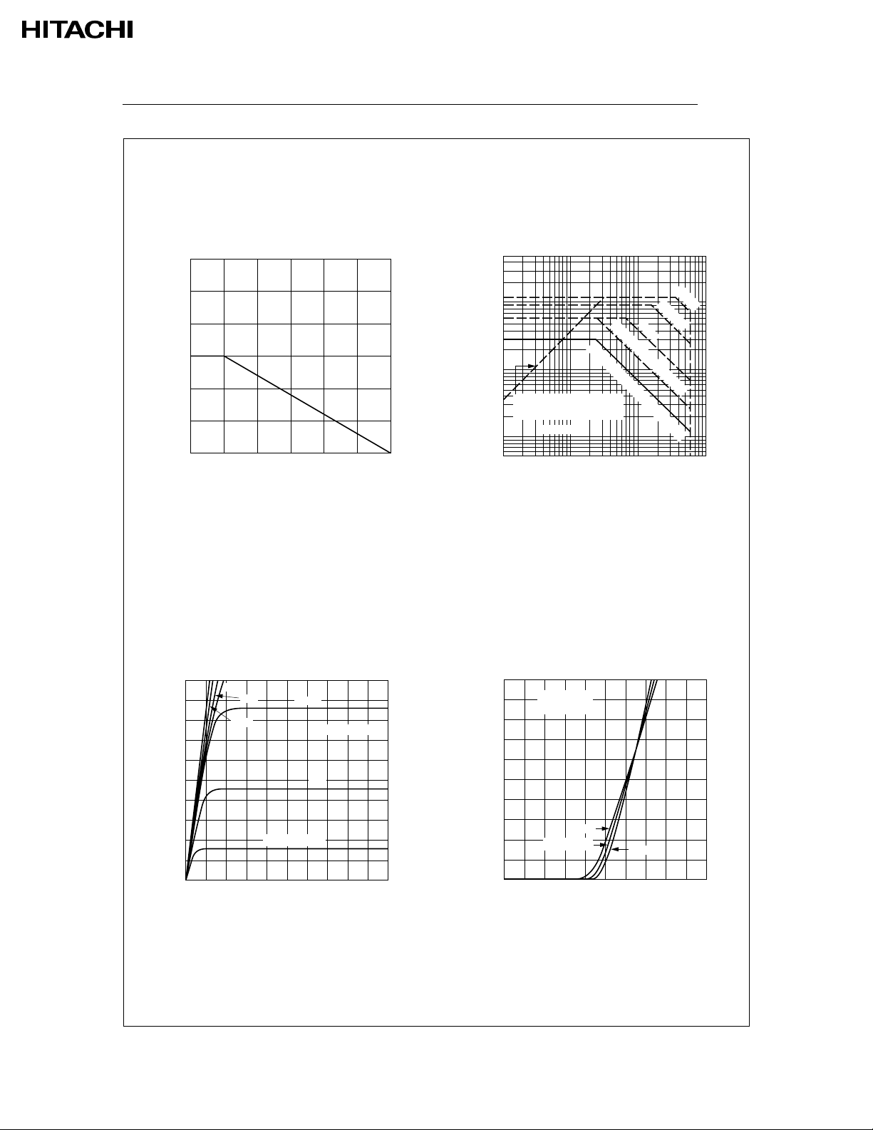
150
100
Channel Dissipation Pch (W)
Power vs. Temperature Derating
50
50 1000
Case Temperature T
(°C)
C
150
500
Maximum Safe Operation Area
200
100
(A)
50
D
20
10
5
Operation in this area
Drain Current I
1.0
0.5
2
0.1
is limited by R
Ta = 25°C
Drain to Source Voltage V
100 µs
1 ms
PW = 10 ms (1 Shot)
DC Operation (T
C
DS (on)
= 25°C)
DS
301031.00.3
(V)
10 µs
100
50
15 V
4 V
5 V
Typical Output Characteristics
40
10 V
30
20
Drain Current ID (A)
10
0
0
Drain to Source Voltage V
3.5 V
3 V
VGS = 2.5 V
6
Pulse Test
842 10
(V)
DS
Typical Transfer Characteristics
50
VDS = 10 V
40
(A)
D
30
Pulse Test
20
Drain Current I
10
TC = 25°C
0
Gate to Source Voltage V
75°C
–25°C
3
42105
(V)
GS
Page 4

2SK1296
Drain to Source Saturation Voltage
vs. Gate to Source Voltage
2.0
1.6
1.2
(V)
(on)
DS
0.8
V
0.4
Drain to Source Saturation Voltage
0
6
Gate to Source Voltage V
0.5
Pulse Test
ID = 50 A
0.2
0.1
(Ω)
0.05
(on)
DS
R
20 A
10 A
842010
(V)
GS
0.02
0.01
0.005
Static Drain to Source on State Resistance
2
Static Drain to Source on State
Resistance vs. Drain Current
Pulse Test
VGS = 4 V
50105 200
20
Drain Current I
D
(A)
10 V
100
Static Drain to Source on State
Resistance vs. Temperature
0.05
ID = 20 A
5 A,10 A
0.04
0.03
(Ω)
(on)
0.02
DS
R
0.01
0
Static Drain to Source on State Resistance
–40
VGS = 4 V
VGS = 10 V
Pulse Test
80
Case Temperature T
5 A,10 A
120400
(°C)
C
20 A
160
1.0
Forward Transfer Admittance yfs (S)
0.5
50
10
20
Forward Transfer Admittance
vs. Drain Current
TC = 25°C
75°C
5
2
1.0 2
Drain Current I
–25°C
5
VDS = 10 V
Pulse Test
10
(A)
D
20
50
Page 5

2SK1296
Body to Drain Diode Reverse
Recovery Time
1000
di/dt = 50 A/µs, Ta = 25°C
(ns)
500
rr
VGS = 0
Pulse Test
200
100
50
20
Reverse Recovery Time t
10
0.5 1.0 5
Reverse Drain Current I
10220
DR
(A)
50
Typical Capacitance vs.
Drain to Source Voltage
10000
1000
100
Capacitance C (pF)
10
01020
Drain to Source Voltage VDS (V)
Ciss
Coss
Crss
30 40
VGS = 0
f = 1 MHz
50
100
Dynamic Input Characteristics
(V)
DS
80
VDD = 100 V
25 V
50 V
60
V
DS
40
20
Drain to Source Voltage V
0 40 120
VDD = 50 V
25 V
10 V
80
Gate Charge Qg (nc)
20
(V)
16
GS
V
GS
12
500
200
100
50
td
(off)
t
f
t
r
8
t
Switching Characteristics
d (on)
Drain Current I
10220
(A)
D
50
ID = 30 A
160
200
4
Gate to Source Voltage V
0
20
Switching Time t (ns)
VGS = 10 V
10
PW = 2 µs, duty < 1 %
5
0.5 1.0 5
Page 6

2SK1296
(A)
DR
50
40
30
20
Reverse Drain Current vs.
Source to Drain Voltage
Pulse Test
10 V
5 V
10
Reverse Drain Current I
0 0.4 1.2
VGS = 0, –5 V
0.8
Source to Drain Voltage V
3
D = 1
1.0
0.5
0.3
0.2
0.1
0.1
0.05
0.02
0.03
0.01
1 Shot Pulse
0.01
10 µ 1 m
Normalized Transient Thermal Impedance γs (t)
100 µ
2.0
1.6
(V)
SD
Normalized Transient Thermal Impedance vs. Pulse Width
θch–c (t) = γs (t) · θch–c
θch–c = 1.67°C/W, T
P
DM
10 m
100 m
Pulse Width PW (s)
TC = 25°C
= 25°C
C
PW
D =
PW
T
T
110
Page 7

2SK1296
Switching Time Test Circuit
Vin Monitor
50 Ω
Vin = 10 V
D.U.T
Vout Monitor
R
L
.
= 30 V
V
.
DD
Vout
t
d (on)
Vin
10 %
10 %
90 %
t
r
Wavewforms
t
d (off)
90 %
90 %
10 %
t
f
 Loading...