

Page 1
1
2
3
查询2SK1093供应商
2SK1093
Silicon N-Channel MOS FET
Application
High speed power switching
Features
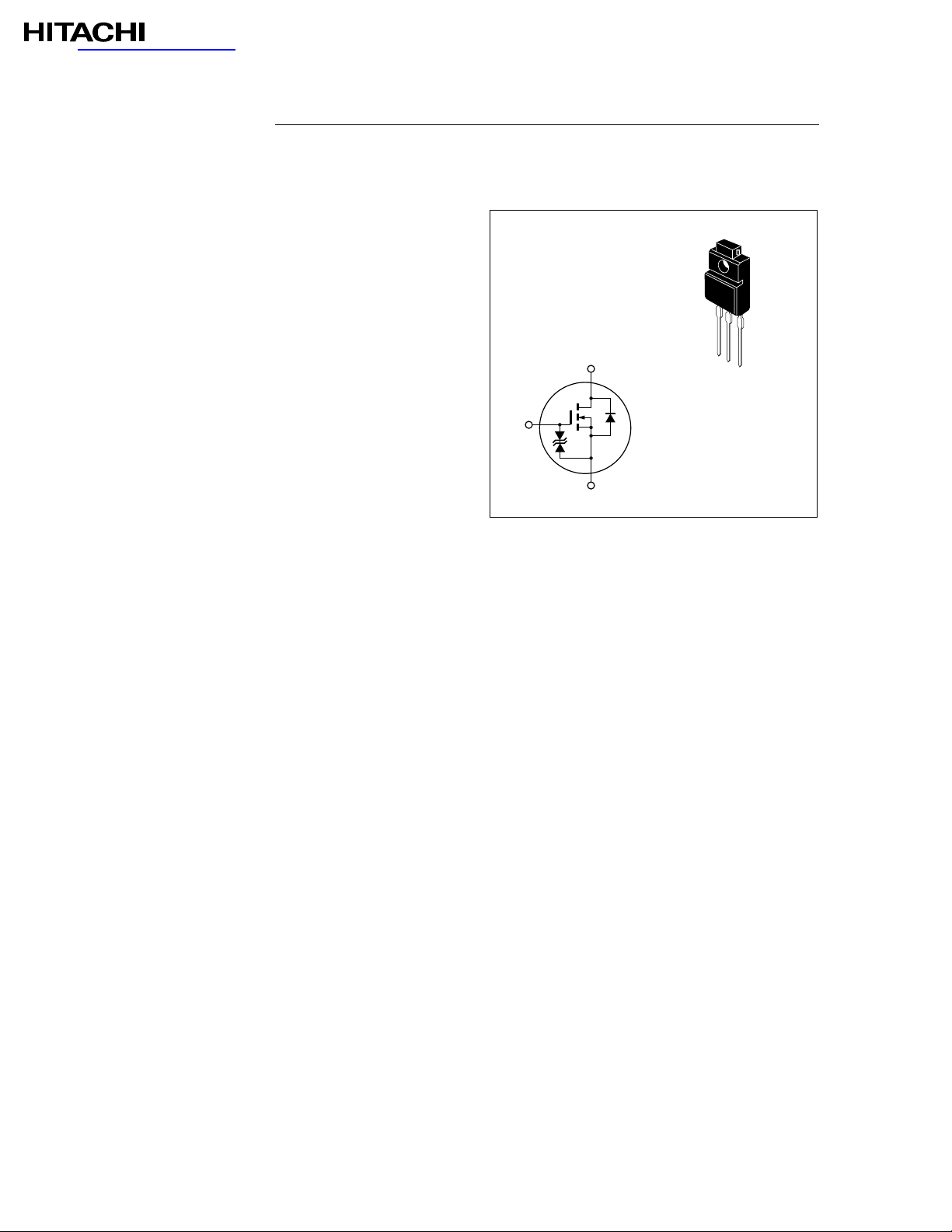
TO–220FM
• Low on-resistance
• High speed switching
2
• Low drive current
• 4 V gate drive device
– Can be driven from 5 V source
• Suitable for motor drive, DC-DC converter,
power switch and solenoid drive
1
1. Gate
2. Drain
3. Source
3
Table 1 Absolute Maximum Ratings (Ta = 25°C)
Item Symbol Ratings Unit
———————————————————————————————————————————
Drain to source voltage V
DSS
60 V
———————————————————————————————————————————
Gate to source voltage V
GSS
±20 V
———————————————————————————————————————————
Drain current I
D
10 A
———————————————————————————————————————————
Drain peak current I
D(pulse)
*40 A
———————————————————————————————————————————
Body to drain diode reverse drain current I
DR
10 A
———————————————————————————————————————————
Channel dissipation Pch** 20 W
———————————————————————————————————————————
Channel temperature Tch 150 °C
———————————————————————————————————————————
Storage temperature Tstg –55 to +150 °C
———————————————————————————————————————————
* PW ≤ 10 µs, duty cycle ≤ 1 %
** Value at T
= 25 °C
C
Page 2

2SK1093
Table 2 Electrical Characteristics (Ta = 25°C)
Item Symbol Min Typ Max Unit Test conditions
———————————————————————————————————————————
Drain to source breakdown V
voltage
(BR)DSS
60 — — V ID= 10 mA, VGS= 0
———————————————————————————————————————————
Gate to source breakdown V
voltage
(BR)GSS
±20 — — V IG= ±100 µA, VDS= 0
———————————————————————————————————————————
Gate to source leak current I
GSS
— — ±10 µA VGS= ±16 V, VDS= 0
———————————————————————————————————————————
Zero gate voltage drain current I
DSS
— — 250 µA VDS= 50 V, VGS= 0
———————————————————————————————————————————
Gate to source cutoff voltage V
GS(off)
1.0 — 2.0 V ID= 1 mA, VDS= 10 V
———————————————————————————————————————————
Static drain to source on state R
resistance
DS(on)
— 0.12 0.15 Ω ID= 5 A, VGS= 10 V *
——————— ——————————–
0.17 0.22 ID= 5 A, VGS= 4 V *
———————————————————————————————————————————
Forward transfer admittance |yfs| 3.5 6.0 — S ID= 5 A, VDS= 10 V *
———————————————————————————————————————————
Input capacitance Ciss — 400 — pF VDS= 10 V, VGS= 0,
————————————————————————————————
Output capacitance Coss — 220 — pF f = 1 MHz
————————————————————————————————
Reverse transfer capacitance Crss — 60 — pF
———————————————————————————————————————————
Turn-on delay time t
d(on)
—5 —nsI
= 5 A, VGS= 10 V,
D
————————————————————————————————
Rise time t
r
— 55 — ns RL= 6 Ω
————————————————————————————————
Turn-off delay time t
d(off)
— 140 — ns
————————————————————————————————
Fall time t
f
—90—ns
———————————————————————————————————————————
Body to drain diode forward V
voltage
DF
— 1.2 — V IF= 10 A, VGS= 0
———————————————————————————————————————————
Body to drain diode reverse t
recovery time di
rr
— 125 — ns IF= 10 A, VGS= 0,
/dt = 50 A/µs
F
———————————————————————————————————————————
* Pulse Test
See characteristic curves of 2SK970.
Page 3

2SK1093
3
1.0
0.3
0.1
0.03
0.01
10 µ 1 m
10 m
100 m
Pulse Width PW (s)
100µ
110
Normalized Transient Thermal Impedance vs. Pulse Width
Normalized Transient Thermal Impedance γ
s
(t)
θch–c (t) = γs (t) · θch–c
θ
ch–c = 6.25°C/W, T
C
= 25°C
P
DM
PW
D =
PW
T
T
TC = 25°C
D = 1
0.5
0.05
1 Shot Pulse
0.2
0.1
0.02
0.01
Channel Dissipation Pch (W)
Power vs. Temperature Derating
30
20
10
50 1000
Case Temperature T
(°C)
C
150
Maximum Safe Operation Area
100
100 µs
PW = 10 ms (1 Shot)
1 ms
(A)
D
30
10
DC Operation (T
3
C
= 25°C)
1.0
Drain Current I
0.3
0.1
Operation in this area
is limited by R
DS (on)
Ta = 25°C
0.1 100
0.3 1.0 3
Drain to Source Voltage V
10
DS
10 µs
30
(V)
 Loading...