

Page 1
2SC4877
Silicon NPN Triple Diffused
Application
TV / character display horizontal deflection output
Features
• High breakdown voltage
V
= 1500 V
CES
• Built–in damper diode type
• Isolated package
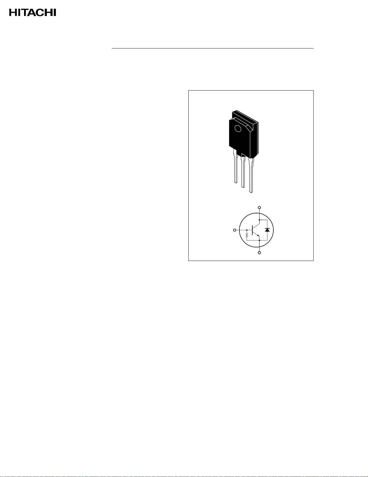
TO-3PFM
TO–3PFM
1. Base
2. Collector
3. Emitter
1
2
3
2
1
3
Absolute Maximum Ratings (Ta = 25°C)
Item Symbol Rating Unit
———————————————————————————————————————————
Collector to emitter voltage V
CES
———————————————————————————————————————————
Emitter to base voltage V
EBO
———————————————————————————————————————————
Collector current I
C
———————————————————————————————————————————
Collector surge current ic(surge) 20 A
———————————————————————————————————————————
Collector power dissipation P
*1
C
———————————————————————————————————————————
Junction temperature T
j
———————————————————————————————————————————
Storage temperature Tstg –55 to +150 °C
———————————————————————————————————————————
C to E diode forward current I
D
———————————————————————————————————————————
Note: 1. Value at TC= 25°C.
1500 V
6V
8A
50 W
150 °C
8A
Page 2

80
60
40
20
0
Collector Power Dissipation Pc (W)
50 100 150 200
Case Temperature Tc (°C)
20
16
12
8
4
400
800 1200 1600 2000
Collector Current I (A)
C
Collector to Emitter Voltage V (V)
CE
0
(100 V, 20 A)
(800 V, 4 A)
0.5 mA
f = 15.75 kHz
Ta = 25 °C
For picture tube arcing
2SC4877
Electrical Characteristics (Ta = 25°C)
Item Symbol Min Typ Max Unit Test Conditions
———————————————————————————————————————————
Emitter to base breakdown V
voltage
(BR)EBO
———————————————————————————————————————————
Collector cutoff current I
CES
———————————————————————————————————————————
DC current transfer ratio h
FE
———————————————————————————————————————————
Collector to emitter saturation V
voltage
CE(sat)
———————————————————————————————————————————
Base to emitter saturation V
voltage
BE(sat)
———————————————————————————————————————————
C to E diode forward voltage V
ECF
———————————————————————————————————————————
Fall time t
f
———————————————————————————————————————————
6 ——VIE= 400 mA, IC= 0
— — 500 µA VCE= 1500 V, RBE= 0
——25—VCE= 5 V, IC= 1 A
——5 VIC= 7 A, IB= 1.4 A
— — 1.5 V IC= 7 A, IB= 1.4 A
— — 3.0 V IF= 8 A
— — 0.5 µs ICP= 7 A, IB1= 1.4 A
I
≈ –2.5 A, fH = 31.5 kHz
B2
Maximum Collector Power Dissipation Curve
Area of Safe Operation
Page 3

Typical Output Characteristics
10
5
0510
Collector to Emitter Voltage V (V)
CE
Collector Current I (A)
C
Tc = 25 °C
I = 0
B
Pc = 50 W
0.2 A
0.4 A
0.6 A
0.8 A
1.0 A
1.2 A
1.4 A
1.6 A
1.8 A
2 A
0.1 0.2 0.5 1 2 5 10
1
5
2
10
20
50
100
DC Current Transfer Ratio h
FE
Collector Current I (A)
C
V = 5 V
CE
Tc = –25°C
25°C
75°C
0.1 0.2 0.5 1 2 5 10
0.05
0.5
1
2
5
Collector to Emitter Saturation Voltage
CE(sat)
0.2
0.1
V (V)
Collector Current I (A)
C
I / I = 5
C B
Tc = –25 °C
25 °C
75 °C
0.2 0.5 1 2 5 100.1
0.5
0.2
1
2
5
10
V (V)
BE(sat)
Base to Emitter Saturetion Voltage
Collector Current I (A)
C
I / I = 5
C B
75 °C
25 °C
Tc = –25 °C
2SC4877
DC Current Transfer Ratio
vs. Collector Current
Collector to Emitter Saturation Voltage
vs. Collector Current
Base to Emitter Saturation Voltage
vs. Collector Current
Page 4

0.1 0.2 0.5 1 2 5 10
Base Current I (A)
B
10
5
0
Collector to Emitter Saturation Voltage
V (V)
CE(sat)
Tc = 25 °C
I = 4 A
C
6 A
8 A
2SC4877
Collector to Emitter Saturation Voltage
vs. Base Current
 Loading...