

Page 1
查询2SA1025, 2SA1081, 2SA1082供应商
2SA1025, 2SA1081, 2SA1082
Silicon PNP Epitaxial
Application
• Low frequency amplifier
• Complementary pair with 2SC2396, 2SC2543 and 2SC2544
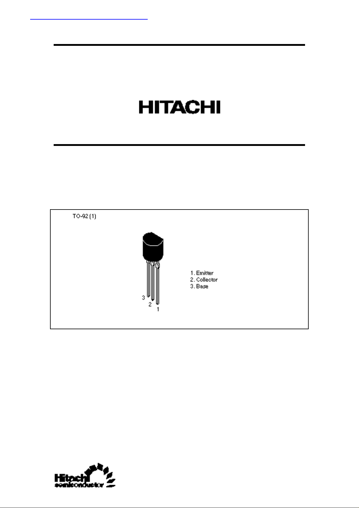
Outline
Page 2
2SA1025, 2SA1081, 2SA1082
2
Absolute Maximum Ratings (Ta = 25°C)
Item Symbol 2SA1025 2SA1081 2SA1082 Unit
Collector to base voltage V
CBO
–60 –90 –120 V
Collector to emitter voltage V
CEO
–60 –90 –120 V
Emitter to base voltage V
EBO
–5 –5 –5 V
Collector current I
C
–100 –100 –100 mA
Emitter current I
E
100 100 100 mA
Collector power dissipation P
C
400 400 400 mW
Junction temperature Tj 150 150 150 °C
Storage temperature Tstg –55 to +150 –55 to +150 –55 to +150 °C
Electrical Characteristics (Ta = 25°C)
2SA1025 2SA1081 2SA1082
Item
CB
= –10 V, IE = 0,
Symbol Min Typ Max Min Typ Max Min Typ Max Unit Test conditions
Collector to base
breakdown voltage
Collector to emitter
breakdown voltage
Emitter to base
breakdown voltage
Collector cutoff current I
Emitter cutoff current I
DC current transfer ratio hFE*
Collector to emitter
saturation voltage
Base to emitter voltage V
Gain bandwidth product f
Collector output
capacitance
Note: 1. The 2SA1025, 2SA1081 and 2SA1082 are grouped by hFE as follows.
D E
250 to 500 400 to 800
V
V
V
CBO
EBO
V
T
–60 — — –90 — — –120 — — V IC = –10 µA, IE = 0
(BR)CBO
–60 — — –90 — — –120 — — V IC = –1 mA,
(BR)CEO
–5 — — –5 — — –5 — — µA IE = –10 µA, IC = 0
(BR)EBO
— — –0.1 — — –0.1 — — –0.1 µA VCB = –50 V, IE = 0
— — –0.1 — — –0.1 — — –0.1 VEB = –2 V, IC = 0
1
250 — 800 250 — 800 250 — 800 VCE = –12 V,
— — –0.2 — — –0.2 — — –0.2 V IC = –10 mA,
CE(sat)
— –0.6 — — –0.6 — — –0.6 — V VCE = –12 V,
BE
— 90 — — 90 — — 90 — MHz VCE = –12 V,
Cob — 3.5 — — 3.5 — — 3.5 — pF V
RBE = ∞
IC = –2 mA
IB = –1 mA
IC = –2 mA
IC = –2 mA
f = 1 MHz
See characteristic curves of 2SA1083.
Page 3

2SA1025, 2SA1081, 2SA1082
3
Page 4

2SA1025, 2SA1081, 2SA1082
4
When using this document, keep the following in mind:
1. This document may, wholly or partially, be subject to change without notice.
2. All rights are reserved: No one is permitted to reproduce or duplicate, in any form, the whole or
part of this document without Hitachi’s permission.
3. Hitachi will not be held responsible for any damage to the user that may result from accidents or
any other reasons during operation of the user’s unit according to this document.
4. Circuitry and other examples described herein are meant merely to indicate the characteristics and
performance of Hitachi’s semiconductor products. Hitachi assumes no responsibility for any
intellectual property claims or other problems that may result from applications based on the
examples described herein.
5. No license is granted by implication or otherwise under any patents or other rights of any third party
or Hitachi, Ltd.
6. MEDICAL APPLICATIONS: Hitachi’s products are not authorized for use in MEDICAL
APPLICATIONS without the written consent of the appropriate officer of Hitachi’s sales company.
Such use includes, but is not limited to, use in life support systems. Buyers of Hitachi’s products
are requested to notify the relevant Hitachi sales offices when planning to use the products in
MEDICAL APPLICATIONS.
 Loading...