

HIT HM62G18512BP-4, HM62G18512BP-5 Datasheet

HM62G18512 Series
8M Synchronous Fast Static RAM
(512k-word × 18-bit)
ADE-203-1185 (Z)
Preliminary
Rev. 0.0
Jun. 12, 2000
Description
The HM62G18512 is a synchronous fast static RAM organized as 512-kword × 18-bit. It has realized high
speed access time by employing the most advanced CMOS process and high speed circuit designing
technology. It is most appropriate for the application which requires high speed, high density memory and
wide bit width configuration, such as cache and buffer memory in system. It is packaged in standard 119bump BGA.
Note: All power supply and ground pins must be connected for proper operation of the device.
Features
• Power supply: 3.3 V +10%, –5%
• Clock frequency: 200 MHz to 250 MHz
• Internal self-timed late write
• Byte write control (2 byte write selects, one for each 9-bit)
• Optional ×36 configuration
• HSTL compatible I/O
• Programmable impedance output drivers
• User selective input trip-point
• Differential, HSTL clock inputs
• Asynchronous G output control
• Asynchronous sleep mode
• Limited set of boundary scan JTAG IEEE 1149.1 compatible
• Protocol: Single clock register-register mode
Preliminary: The specifications of this device are subject to change without notice. Please contact your
nearest Hitachi’s Sales Dept. regarding specifications.
HM62G18512 Series
Ordering Information
Type No. Access time Cycle time Package
HM62G18512BP-4
HM62G18512BP-5
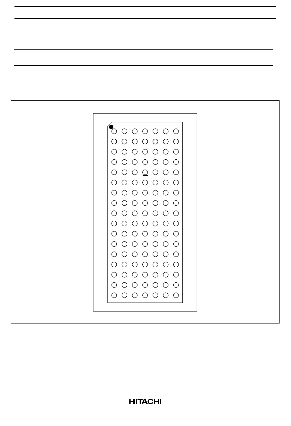
Pin Arrangement
2.1 ns
2.5 ns
4.0 ns
5.0 ns
119-bumps BGA
1234567
A
VDDQ SA0 SA6 NC SA4 SA2 VDDQ
B
NC NC SA7 NC SA8 SA18 NC
C
NC SA13 SA3 VDD SA5 SA1 NC
D
DQb0 NC VSS ZQ VSS DQa4 NC
E
NC DQb1 VSS SS VSS NC DQa5
F
VDDQ NC VSS G VSS DQa6 VDDQ
G
NC DQb2 SWEb NC NC DQa7
H
DQb3 NC VSS NC VSS DQa8 NC
J
VDDQ VDD VREF VDD VREF VDD VDDQ
K
NC DQb8 VSS K VSS NC DQa3
L
DQb7 NC K SWEa DQa2 NC
M
VDDQ DQb6 VSS SWE VSS NC VDDQ
N
DQb5 NC VSS SA16 VSS DQa1 NC
P
NC DQb4 VSS SA14 VSS NC DQa0
R
NC SA9 M1 VDD M2 SA10 NC
T
NC SA17 SA11 NC SA12 SA15 ZZ
U
VDDQ TMS TDI TCK TDO NC VDDQ
VSS
VSS
119-bump 1. 27 mm
14 mm × 22 mm BGA (BP-119A)
(Top view)
2
HM62G18512 Series
Pin Description
Name I/O type Descriptions Notes
V
DD
V
SS
V
DDQ
V
REF
K Input Clock input. Active high.
K Input Clock input. Active low.
SS Input Synchronous chip select
SWE Input Synchronous write enable
SAn Input Synchronous address input n = 0, 1, 2...18
SWEx Input Synchronous byte write enables x = a, b
G Input Asynchronous output enable
ZZ Input Power down mode select
ZQ Input Output impedance control 1
DQxn I/O Synchronous data input/output x = a, b
M1, M2 Input Output protocol mode select
TMS Input Boundary scan test mode select
TCK Input Boundary scan test clock
TDI Input Boundary scan test data input
TDO Output Boundary scan test data output
NC — No connection
Supply Core power supply
Supply Ground
Supply Output power supply
Supply Input reference: provides input reference voltage
n = 0, 1, 2...8
M1 M2 Protocol Notes
V
SS
V
DD
Synchronous register to register operation 2
Notes: 1. ZQ is to be connected to VSS via a resistance RQ where 150 Ω ≤ RQ ≤ 300 Ω, if ZQ = V
open, output buffer impedance will be maximum. A case of minimum impedance, it needs to
connect over 120 Ω between ZQ and V
2. There is 1 protocol with mode pin. Mode control pins (M1, M2) are to be tied either V
.
SS
DD
respectively. The state of the Mode control inputs must be set before power-up and must not
change during device operation. Mode control inputs are not standard inputs and may not meet
V
or VIL specification. This SRAM is tested only in the synchronous register to register
IH
operation.
DDQ
or V
or
SS
3
HM62G18512 Series
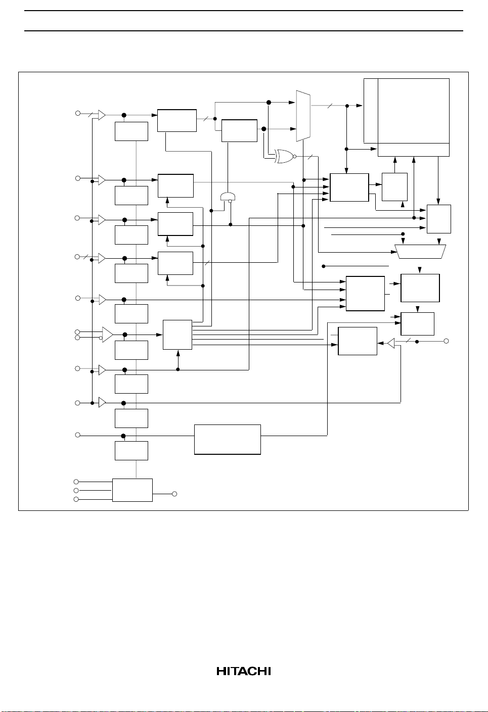
Block Diagram
A0 to A18
SS
SWE
SWEx
ZZ
V
REF
ZQ
19
JTAG
register
JTAG
register
JTAG
register
2
JTAG
register
G
K
K
JTAG
register
JTAG
register
JTAG
register
JTAG
register
JTAG
register
R-Add
register
SS
register
SWE
register
SWEx
register
CLK
control
19
W-Add
register
2
Impedance
contorol logic
19
MUX
1
WRC
Match
DOC
D-in
register
Memory
cell array
(512k × 18)
Row decoder
Column decoder
WA
Multiplex
D-out
register
OB
18
SA
DQa0-8
DQb0-8
TDI
TCK
TMS
JTAG tap
controller
TDO
4
HM62G18512 Series
Operation Table
ZZ SS G SWE SWEa SWEb K K Operation DQ (n) DQ (n + 1)
H ЧЧЧЧЧЧЧsleep mode High-Z High-Z
LH××××L-H H-L Dead
(not selected)
L × H ЧЧЧЧЧDead
(Dummy read)
LLLH××L-H H-L Read × Dout
LL× L L L L-H H-L Write a, b byte High-Z Din (a,b)0-8
LL× L L H L-H H-L Write a byte High-Z Din (a)0-8
LL× L H L L-H H-L Write b byte High-Z Din (b)0-8
Notes: 1. × means don’t care for synchronous inputs, and H or L for asynchronous inputs.
2. SWE, SS, SWEa to SWEb , SA are sampled at the rising edge of K clock.
3. Although differential clock operation is implied, this SRAM will operate properly with one clock
phase (either K or K) tied to V
specified within this document will be met.
. Under such single-ended clock operation, all parameters
REF
× High-Z
High-Z High-Z
(a,b)0-8
5
HM62G18512 Series
Absolute Maximum Ratings
Parameter Symbol Value Unit Notes
Input voltage on any pin V
Core supply voltage V
Output supply voltage V
Operating temperature T
Storage temperature T
IN
DD
DDQ
OPR
STG
–0.5 to V
–0.5 to 3.9 V 1
–0.5 to 2.2 V 1, 4
0 to 70 °C
–55 to 125 °C
Junction temperature Tj 110 °C
Output short–circuit current I
Latch up current I
OUT
LI
25 mA
200 mA
Package junction to case thermal resistance θJC 2 °C/W 5, 7
Package junction to ball thermal resistance θJB 5 °C/W 6, 7
Notes: 1. All voltage is referred to VSS.
2. Permanent device damage may occur if Absolute Maximum Ratings are exceeded. Functional
operation should be restricted the Operation Conditions. Exposure to higher than recommended
voltages for extended periods of time could affect device reliability.
3. These CMOS memory circuits have been designed to meet the DC and AC specifications shown
in the tables after thermal equilibrium has been established.
4. The supply voltage application sequence need to be powered up in the following manner: V
V
, V
, V
DD
DDQ
then VIN. Remember, according to the Absolute Maximum Ratings table, V
REF
not to exceed 3.9 V, whatever the instantaneous value of V
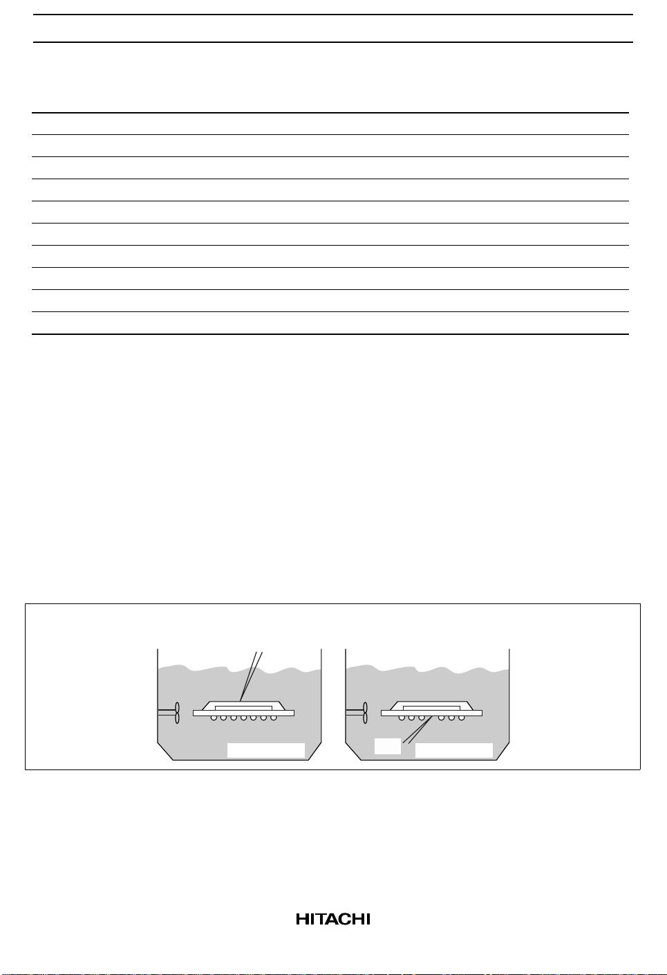
5. θJC is measured at the center of mold surface in fluorocarbon (See Figure “Definition of
Measurement”).
6. θJB is measured on the center ball pad after removing the ball in fluorocarbon (See Figure
“Definition of Measurement”).
7. These thermal resistance values have error of ± 5°C/W.
+ 0.5 V 1, 4
DDQ
.
DDQ
DDQ
,
SS
is
θJC
θJB
T.C.
Fluorocarbon
T.C.
Fluorocarbon
Definition of Measurement
6
HM62G18512 Series
Note: The following the DC and AC specifications shown in the Tables, this device is tested under the
minimum transverse air flow exceeding 500 linear feet per minute.
DC Operating Conditions (Ta = 0 to 70°C [Tj max = 110°C])
Parameter Symbol Min Typ Max Unit Notes
Supply voltage (Core) V
Supply voltage (I/O) V
Supply voltage V
Input reference voltage (I/O) V
Input high voltage V
Input low voltage V
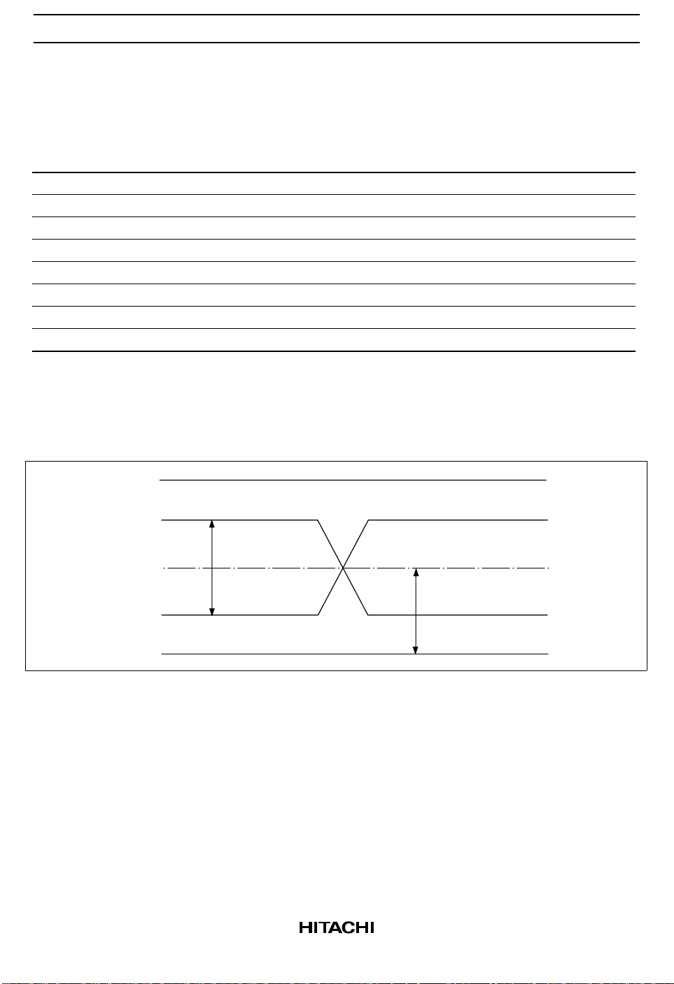
Clock differential voltage V
Clock common mode voltage V
DD
DDQ
SS
REF
IH
IL
DIF
CM
Notes: 1. Peak to peak AC component superimposed on V
2. Minimum differential input voltage required for differential input clock operation.
3. See following figure.
4. V
= 0.75 V (typ).
REF
3.135 3.30 3.63 V
1.4 1.5 1.6 V
000 V
0.65 0.75 0.90 V 1
V
+ 0.1 — V
REF
–0.5 — V
0.1 — V
+ 0.3 V 4
DDQ
– 0.1 V 4
REF
+ 0.3 V 2, 3
DDQ
0.55 — 0.90 V 3
may not exceed 5% of V
REF
REF
.
V
DDQ
V
SS
V
DIF
V
CM
Differential Voltage/Common Mode Voltage
7
 Loading...