

HIT HM628512CLRR-7, HM628512CLRR-7SL, HM628512CLTT-5, HM628512CLTT-5SL, HM628512CLTT-7 Datasheet
...
HM628512C Series
4 M SRAM (512-kword × 8-bit)
ADE-203-1212 (Z)
Preliminary
Rev. 0.0
Sep. 12, 2000
Description
The Hitachi HM628512C is a 4-Mbit static RAM organized 512-kword × 8-bit. It realizes higher density,
higher performance and low power consumption by employing Hi-CMOS process technology. The device,
packaged in a 525-mil SOP (foot print pitch width) or 400-mil TSOP TYPE II or 600-mil plastic DIP, is
available for high density mounting. The HM628512C is suitable for battery backup system.
Features
• Single 5 V supply
• Access time: 55/70 ns (max)
• Power dissipation
Active: 50 mW/MHz (typ)
Standby: 10 µW (typ)
• Completely static memory. No clock or timing strobe required
• Equal access and cycle times
• Common data input and output: Three state output
• Directly TTL compatible: All inputs and outputs
• Battery backup operation
Preliminary: The specification of this device are subject to change without notice. Please contact your
nearest Hitachi’s Sales Dept. regarding specification.
HM628512C Series
Ordering Information
Type No. Access time Package
HM628512CLP-5
HM628512CLP-7
HM628512CLP-5SL
HM628512CLP-7SL
HM628512CLFP-5
HM628512CLFP-7
HM628512CLFP-5SL
HM628512CLFP-7SL
HM628512CLTT-5
HM628512CLTT-7
HM628512CLTT-5SL
HM628512CLTT-7SL
HM628512CLRR-5
HM628512CLRR-7
HM628512CLRR-5SL
HM628512CLRR-7SL
55 ns
70 ns
55 ns
70 ns
55 ns
70 ns
55 ns
70 ns
55 ns
70 ns
55 ns
70 ns
55 ns
70 ns
55 ns
70 ns
600-mil 32-pin plastic DIP (DP-32)
525-mil 32-pin plastic SOP (FP-32D)
400-mil 32-pin plastic TSOP II (TTP-32D)
400-mil 32-pin plastic TSOP II reverse (TTP-32DR)
2
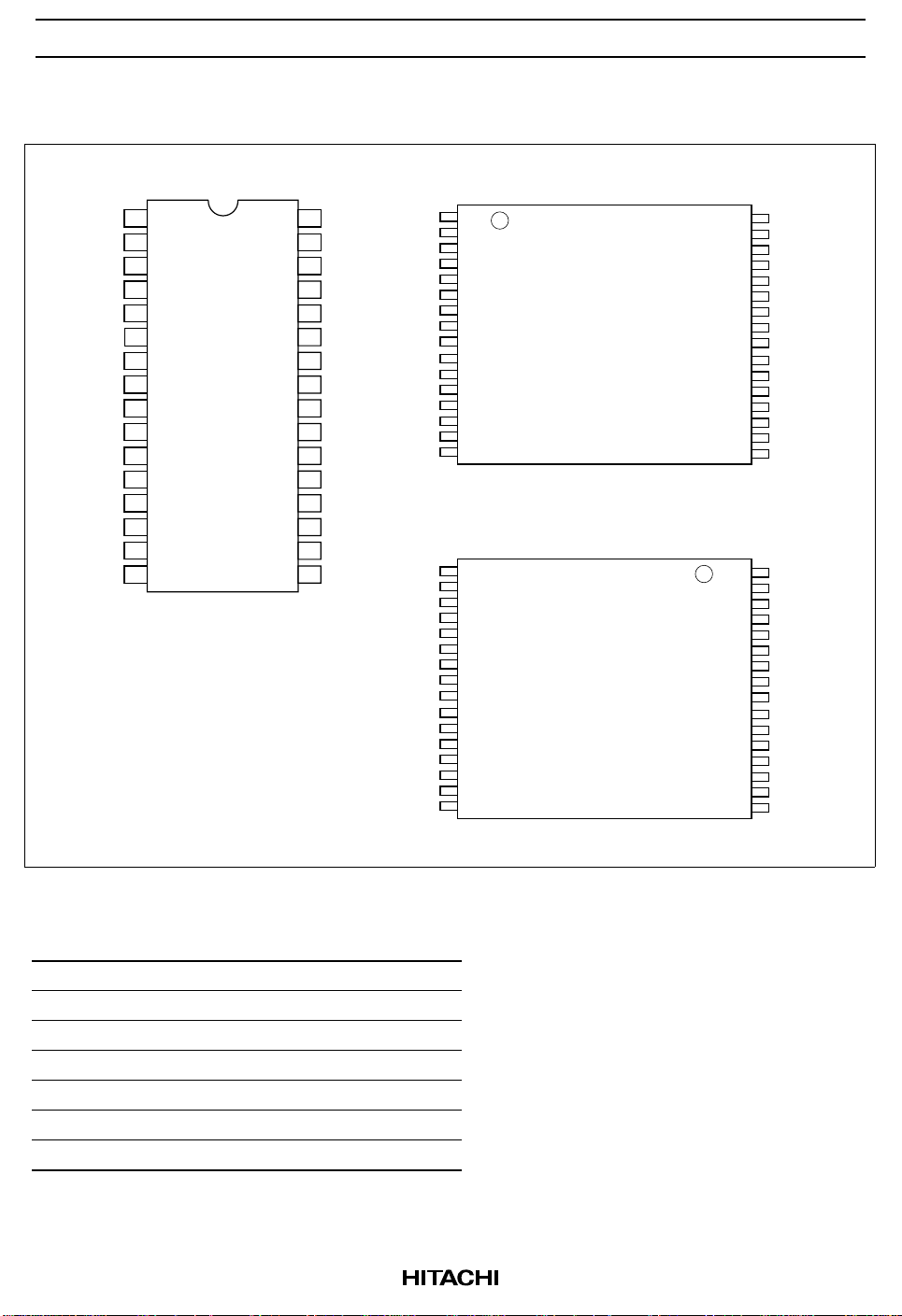
Pin Arrangement
HM628512C Series
A18
A16
A14
A12
A7
A6
A5
A4
A3
A2
A1
A0
I/O0
I/O1
I/O2
V
SS
32-pin DIP
32-pin SOP
1
2
3
4
5
6
7
8
9
10
11
12
13
14
15
16
(Top view)
32
31
30
29
28
27
26
25
24
23
22
21
20
19
18
17
V
CC
A15
A17
WE
A13
A8
A9
A11
OE
A10
CS
I/O7
I/O6
I/O5
I/O4
I/O3
A18
A16
A14
A12
A7
A6
A5
A4
A3
A2
A1
A0
I/O0
I/O1
I/O2
V
SS
V
CC
A15
A17
WE
A13
A8
A9
A11
OE
A10
CS
I/O7
I/O6
I/O5
I/O4
I/O3
1
2
3
4
5
6
7
8
9
10
11
12
13
14
15
16
32
31
30
29
28
27
26
25
24
23
22
21
20
19
18
17
32-pin TSOP
(Top view)
32-pin TSOP (reverse)
32
31
30
29
28
27
26
25
24
23
22
21
20
19
18
17
1
2
3
4
5
6
7
8
9
10
11
12
13
14
15
16
V
CC
A15
A17
WE
A13
A8
A9
A11
OE
A10
CS
I/O7
I/O6
I/O5
I/O4
I/O3
A18
A16
A14
A12
A7
A6
A5
A4
A3
A2
A1
A0
I/O0
I/O1
I/O2
V
SS
Pin Description
Pin name Function
A0 to A18 Address input
I/O0 to I/O7 Data input/output
CS Chip select
OE Output enable
WE Write enable
V
CC
V
SS
Power supply
Ground
(Top view)
3
HM628512C Series
Block Diagram
LSB
MSB
A11
A9
A8
A15
A18
A10
A13
A17
A16
A14
A12
I/O0
I/O7
Row
Decoder
Input
Data
Control
•
•
•
•
•
•
•
LSB
Memory Matrix
2,048 2,048
Column Decoder
A3A2A1A0 A6A5
•
•
×
Column I/O
A4 A7
MSB
V
CC
V
SS
•
•
CS
WE
OE
4
Timing Pulse Generator
Read/Write Control
HM628512C Series
Function Table
WE CS OE Mode VCC current Dout pin Ref. cycle
× H × Not selected I
H L H Output disable I
H L L Read I
L L H Write I
L L L Write I
, I
SB
SB1
CC
CC
CC
CC
Note: ×: H or L
Absolute Maximum Ratings
Parameter Symbol Value Unit
Power supply voltage V
Voltage on any pin relative to V
SS
Power dissipation P
CC
V
T
T
Operating temperature Topr –20 to +70 °C
Storage temperature Tstg –55 to +125 °C
Storage temperature under bias Tbias –20 to +85 °C
Notes: 1. VT min: –3.0 V for pulse half-width ≤ 30 ns.
2. Maximum voltage is 7.0 V.
–0.5 to +7.0 V
–0.5*1 to VCC + 0.3*
1.0 W
High-Z —
High-Z —
Dout Read cycle
Din Write cycle (1)
Din Write cycle (2)
2
V
Recommended DC Operating Conditions (Ta = –20 to +70°C)
Parameter Symbol Min Typ Max Unit
Supply voltage V
Input high voltage V
Input low voltage V
CC
V
SS
IH
IL
Note: 1. VIL min: –3.0 V for pulse half-width ≤ 30 ns.
4.5 5.0 5.5 V
000V
2.2 — VCC + 0.3 V
*1
–0.3
— 0.8 V
5
HM628512C Series
DC Characteristics (Ta = –20 to +70°C, VCC = 5 V ±10% , VSS = 0 V)
Parameter Symbol Min Typ*1Max Unit Test conditions
Input leakage current |I
Output leakage current |ILO|——1µA CS = VIH or OE = VIH or
Operating power supply current: DC I
Operating power supply current I
Operating power supply current I
Standby power supply current: DC I
Standby power supply current (1): DC I
Output low voltage V
Output high voltage V
Notes: 1. Typical values are at VCC = 5.0 V, Ta = +25°C and specified loading, and not guaranteed.
2. This characteristics is guaranteed only for L version.
3. This characteristics is guaranteed only for L-SL version.
|——1µA Vin = VSS to V
LI
WE = V
CC
— 8 15 mA CS = VIL,
IL
others = V
CC1
CC2
— 40 60 mA Min cycle, duty = 100%
CS = V
I
I/O
, others = VIH/V
IL
= 0 mA
— 10 20 mA Cycle time = 1 µs,
duty = 100%
I
= 0 mA, CS ≤ 0.2 V
I/O
V
≥ VCC – 0.2 V, VIL ≤ 0.2 V
IH
SB
SB1
—1 3 mACS = V
IH
—2*2100*2µA Vin ≥ 0 V, CS ≥ VCC – 0.2 V
—2*350*3µA
OL
OH
— — 0.4 V IOL = 2.1 mA
2.4 — — V IOH = –1.0 mA
, V
I/O
IH/VIL
CC
= VSS to V
, I
= 0 mA
I/O
CC
IL
Capacitance (Ta = +25°C, f = 1 MHz)
Parameter Symbol Typ Max Unit Test conditions
Input capacitance*
1
Input/output capacitance*1C
Note: 1. This parameter is sampled and not 100% tested.
Cin — 8 pF Vin = 0 V
I/O
—10pFV
= 0 V
I/O
6

HM628512C Series
AC Characteristics (Ta = –20 to +70°C, VCC = 5 V ± 10%, unless otherwise noted.)
Test Conditions
• Input pulse levels: 0.8 V to 2.4 V
• Input rise and fall time: 5 ns
• Input and output timing reference levels: 1.5 V
• Output load: 1 TTL Gate + CL (100 pF) (HM628512C-7)
1 TTL Gate + CL (50 pF) (HM628512C-5)
(Including scope & jig)
Read Cycle
HM628512C
-5 -7
Parameter Symbol Min Max Min Max Unit Notes
Read cycle time t
Address access time t
Chip select access time t
Output enable to output valid t
Chip selection to output in low-Z t
Output enable to output in low-Z t
Chip deselection to output in high-Z t
Output disable to output in high-Z t
Output hold from address change t
RC
AA
CO
OE
LZ
OLZ
HZ
OHZ
OH
55 — 70 — ns
— 55 — 70 ns
— 55 — 70 ns
— 25 — 35 ns
10 — 10 — ns 2
5 — 5 — ns 2
0 20 0 25 ns 1, 2
0 20 0 25 ns 1, 2
10 — 10 — ns
7

HM628512C Series
Write Cycle
HM628512C
-5 -7
Parameter Symbol Min Max Min Max Unit Notes
Write cycle time t
Chip selection to end of write t
Address setup time t
Address valid to end of write t
Write pulse width t
Write recovery time t
WE to output in high-Z t
Data to write time overlap t
Data hold from write time t
Output active from output in high-Z t
Output disable to output in high-Z t
Notes: 1. tHZ, t
OHZ
and t
are defined as the time at which the outputs achieve the open circuit conditions and
WHZ
are not referred to output voltage levels.
2. This parameter is sampled and not 100% tested.
3. A write occurs during the overlap (t
transition of CS going low or WE going low. A write ends at the earlier transition of CS going high
or WE going high. t
4. t
is measured from CS going low to the end of write.
CW
5. t
is measured from the address valid to the beginning of write.
AS
6. t
is measured from the earlier of WE or CS going high to the end of write cycle.
WR
is measured from the beginning of write to the end of write.
WP
7. During this period, I/O pins are in the output state so that the input signals of the opposite phase to
the outputs must not be applied.
8. If the CS low transition occurs simultaneously with the WE low transition or after the WE transition,
the output remain in a high impedance state.
9. Dout is the same phase of the write data of this write cycle.
10.Dout is the read data of next address.
11.If CS is low during this period, I/O pins are in the output state. Therefore, the input signals of the
opposite phase to the outputs must not be applied to them.
12.In the write cycle with OE low fixed, t
data bus contention. t
≥ tDW min + t
WP
WC
CW
AS
AW
WP
WR
WHZ
DW
DH
OW
OHZ
55 — 70 — ns
50 — 60 — ns 4
0 — 0 — ns 5
50 — 60 — ns
40 — 50 — ns 3, 12
0 — 0 — ns 6
0 20 0 25 ns 1, 2, 7
25 — 30 — ns
0—0—ns
5 — 5 — ns 2
0 20 0 25 ns 1, 2, 7
) of a low CS and a low WE. A write begins at the later
WP
must satisfy the following equation to avoid a problem of
WP
max
WHZ
8

Timing Waveforms
Read Timing Waveform (WE = VIH)
Address
CS
OE
HM628512C Series
t
RC
t
AA
t
CO
t
LZ
t
OE
t
OLZ
t
HZ
t
OHZ
Dout
Valid Data
t
OH
9

HM628512C Series
Write Timing Waveform (1) (OE Clock)
Address
t
WC
OE
CS
WE
Dout
Din
t
AW
t
CW
*8
t
AS
t
OHZ
t
WP
t
DW
t
WR
t
DH
Valid Data
10

Write Timing Waveform (2) (OE Low Fixed)
Address
t
HM628512C Series
WC
CS
WE
Dout
Din
t
CW
*8
t
AW
t
WP
t
AS
t
WHZ
t
DW
t
DH
t
WR
t
OW
t
OH
*9
*11
*10
Valid Data
11
HM628512C Series
Low VCC Data Retention Characteristics (Ta = –20 to +70°C)
Parameter Symbol Min Typ Max Unit Test conditions*
VCC for data retention V
Data retention current I
DR
CCDR
2——V CS ≥ VCC – 0.2 V, Vin ≥ 0 V
—1*450*1µAVCC = 3.0 V, Vin ≥ 0 V
CS ≥ V
– 0.2 V
CC
—1*415*2µA
Chip deselect to data retention time t
Operation recovery time t
CDR
R
0 — — ns See retention waveform
tRC*5—— ns
Notes: 1. For L-version and 20 µA (max.) at Ta = –20 to +40°C.
2. For L-SL-version and 3 µA (max.) at Ta = –20 to +40°C.
3. CS controls address buffer, WE buffer, OE buffer, and Din buffer. In data retention mode, Vin
levels (address, WE, OE, I/O) can be in the high impedance state.
4. Typical values are at V
= read cycle time.
5. t
RC
= 3.0 V, Ta = +25°C and specified loading, and not guaranteed.
CC
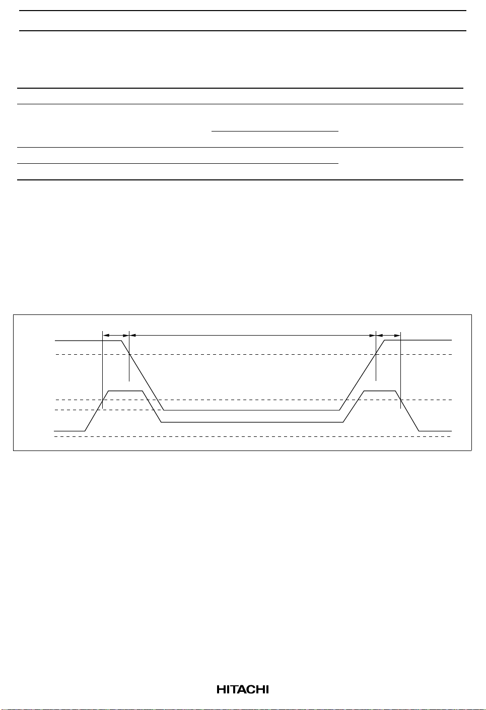
Low VCC Data Retention Timing Waveform (CS Controlled)
t
R
V
CC
4.5 V
t
CDR
Data retention mode
3
2.2 V
V
DR
CS
0 V
CS ≥ VCC – 0.2 V
12

Package Dimensions
HM628512CLP Series (DP-32)
32 17
HM628512C Series
Unit: mm
41.90
42.50 Max
13.4
13.7 Max
1
2.30 Max
2.54 ± 0.25
1.20
0.48 ± 0.10
16
5.08 Max
2.54 Min
0.51 Min
Hitachi Code
JEDEC
EIAJ
Mass
15.24
0.25
0° – 15°
(reference value)
+ 0.11
– 0.05
DP-32
—
Conforms
5.1 g
13

HM628512C Series
Package Dimensions (cont.)
HM628512CLFP Series (FP-32D)
20.45
20.95 Max
32
Unit: mm
17
11.30
1
1.00 Max
0.15
0.10
M
1.27
*0.40 ± 0.08
0.38 ± 0.06
*Dimension including the plating thickness
Base material dimension
16
+ 0.12
– 0.10
0.15
3.00 Max
0.20 ± 0.04
*0.22 ± 0.05
Hitachi Code
JEDEC
EIAJ
Mass
(reference value)
14.14 ± 0.30
1.42
0° – 8°
0.80 ± 0.20
FP-32D
Conforms
—
1.3 g
14

Package Dimensions (cont.)
HM628512CLTT Series (TTP-32D)
20.95
21.35 Max
32
HM628512C Series
Unit: mm
17
10.16
1
*0.42 ± 0.08
0.40 ± 0.06
1.15 Max
1.20 Max
*Dimension including the plating thickness
Base material dimension
0.21
0.10
1.27
M
16
*0.17 ± 0.05
0.125 ± 0.04
11.76 ± 0.20
0.13 ± 0.05
Hitachi Code
JEDEC
EIAJ
Mass
(reference value)
0° – 5°
0.80
0.50 ± 0.10
TTP-32D
Conforms
—
0.51 g
15

HM628512C Series
Package Dimensions (cont.)
HM628512CLRR Series (TTP-32DR)
20.95
21.35 Max
1
Unit: mm
16
10.16
32
*0.42 ± 0.08
0.40 ± 0.06
1.15 Max
1.20 Max
*Dimension including the plating thickness
Base material dimension
0.21
0.10
1.27
M
17
*0.17 ± 0.05
0.125 ± 0.04
11.76 ± 0.20
0.13 ± 0.05
Hitachi Code
JEDEC
EIAJ
Mass
(reference value)
0° – 5°
0.80
0.50 ± 0.10
TTP-32DR
Conforms
—
0.51 g
16

HM628512C Series
Cautions
1. Hitachi neither warrants nor grants licenses of any rights of Hitachi’s or any third party’s patent,
copyright, trademark, or other intellectual property rights for information contained in this document.
Hitachi bears no responsibility for problems that may arise with third party’s rights, including intellectual
property rights, in connection with use of the information contained in this document.
2. Products and product specifications may be subject to change without notice. Confirm that you have
received the latest product standards or specifications before final design, purchase or use.
3. Hitachi makes every attempt to ensure that its products are of high quality and reliability. However,
contact Hitachi’s sales office before using the product in an application that demands especially high
quality and reliability or where its failure or malfunction may directly threaten human life or cause risk of
bodily injury, such as aerospace, aeronautics, nuclear power, combustion control, transportation, traffic,
safety equipment or medical equipment for life support.
4. Design your application so that the product is used within the ranges guaranteed by Hitachi particularly for
maximum rating, operating supply voltage range, heat radiation characteristics, installation conditions and
other characteristics. Hitachi bears no responsibility for failure or damage when used beyond the
guaranteed ranges. Even within the guaranteed ranges, consider normally foreseeable failure rates or
failure modes in semiconductor devices and employ systemic measures such as fail-safes, so that the
equipment incorporating Hitachi product does not cause bodily injury, fire or other consequential damage
due to operation of the Hitachi product.
5. This product is not designed to be radiation resistant.
6. No one is permitted to reproduce or duplicate, in any form, the whole or part of this document without
written approval from Hitachi.
7. Contact Hitachi’s sales office for any questions regarding this document or Hitachi semiconductor
products.
Hitachi, Ltd.
Semiconductor & Integrated Circuits.
Nippon Bldg., 2-6-2, Ohte-machi, Chiyoda-ku, Tokyo 100-0004, Japan
Tel: Tokyo (03) 3270-2111 Fax: (03) 3270-5109
URL NorthAmerica : http://semiconductor.hitachi.com/
Europe : http://www.hitachi-eu.com/hel/ecg
Asia : http://www.hitachi.com.sg/grp3/sicd
Japan : http://www.hitachi.co.jp/Sicd/indx.htm
For further information write to:
Hitachi Semiconductor
(America) Inc.
179 East Tasman Drive,
San Jose,CA 95134
Tel: <1> (408) 433-1990
Fax: <1>(408) 433-0223
Hitachi Europe GmbH
Electronic Components Group
Dornacher Straße 3
D-85622 Feldkirchen, Munich
Germany
Tel: <49> (89) 9 9180-0
Fax: <49> (89) 9 29 30 00
Hitachi Europe Ltd.
Electronic Components Group.
Whitebrook Park
Lower Cookham Road
Maidenhead
Berkshire SL6 8YA, United Kingdom
Tel: <44> (1628) 585000
Fax: <44> (1628) 585160
Hitachi Asia Ltd.
16 Collyer Quay #20-00
Hitachi Tower
Singapore 049318
Tel: 535-2100
Fax: 535-1533
Hitachi Asia Ltd.
Taipei Branch Office
3rd Flr, Hung Kuo Building, No.167,
Tun Hwa North Road, Taipei (105)
Taiwan
Tel: <886> (2) 2718-3666
Fax: <886> (2) 2718-8180
Telex: 23222 HAS-TP
Copyright © Hitachi, Ltd., 2000. All rights reserved. Printed in Japan.
Hitachi Asia (Hong Kong) Ltd.
Group III (Electronic Components)
7th Flr, North Tower, World Finance Centre,
Harbour City, Canton Road, Tsim Sha Tsui,
Kowloon, Hong Kong
Tel: <852> (2) 735 9218
Fax: <852> (2) 730 0281
Telex: 40815 HITEC HX
Colophon 1.0
17
 Loading...