


Preliminary: The Specifications of this device are subject to change without notice. Please contact to your
nearest Hitachi’s sales Dept. regarding specifications
HM5164165 Series
HM5165165 Series
64M EDO DRAM (4-Mword × 16-bit)
8k refresh/4k refresh
ADE-203-802A(Z)
Preliminary
Rev. 0.1
Oct. 24, 1997
Description
The Hitachi HM5164165 Series, HM5165165 Series are 64M-bit dynamic RAMs organized as 4,194,304word × 16-bit. They have realized high performance and low power by employing CMOS process technology.
HM5164165 Series, HM5165165 Series offer Extended Data Out (EDO) Page Mode as a high speed access
mode. They have the package variations of standard 50-pin plastic SOJ and standerd 50-pin plastic TSOPII
Features
• Single 3.3 V supply: 3.3 V ± 0.3 V
• Access time: 50 ns/60 ns (max)
• Power dissipation
Active: 432 mW/396 mW (max) (HM5164165 Series)
: 504 mW/432 mW (max) (HM5165165 Series)
Standby : 1.8 mW (max) (CMOS interface)
: 0.54 mW (max) (L-version)
• EDO page mode capability
• Refresh cycles
RAS-only refresh
8192 cycles/64 ms (HM5164165)
/128 ms (HM5164165L) (L-version)
4096 cycles/64 ms (HM5165165)
/128 ms (HM5165165L) (L-version)
CBR/Hidden refresh
4096 cycles/64 ms (HM5164165, HM5165165)
/128 ms (HM5164165L, HM5165165L) (L-version)
HM5164165 Series, HM5165165 Series
2
• 4 variations of refresh
RAS-only refresh
CAS-before-RAS refresh
Hidden refresh
Self refresh (L-version)
• 2CAS-byte control
• Battery backup operation (L-version)
Ordering Information
Type No. Access time Package
HM5164165J-5*
HM5164165J-6*
50 ns
60 ns
400-mil 50-pin plastic SOJ (CP-50DA)
HM5164165LJ-5*
HM5164165LJ-6*
50 ns
60 ns
HM5165165J-5*
HM5165165J-6*
50 ns
60 ns
HM5165165LJ-5*
HM5165165LJ-6*
50 ns
60 ns
HM5164165TT-5
HM5164165TT-6
50 ns
60 ns
400-mil 50-pin plastic TSOP II (TTP-50DB)
HM5164165LTT-5
HM5164165LTT-6
50 ns
60 ns
HM5165165TT-5
HM5165165TT-6
50 ns
60 ns
HM5165165LTT-5
HM5165165LTT-6
50 ns
60 ns
Note: Under development.
HM5164165 Series, HM5165165 Series
3
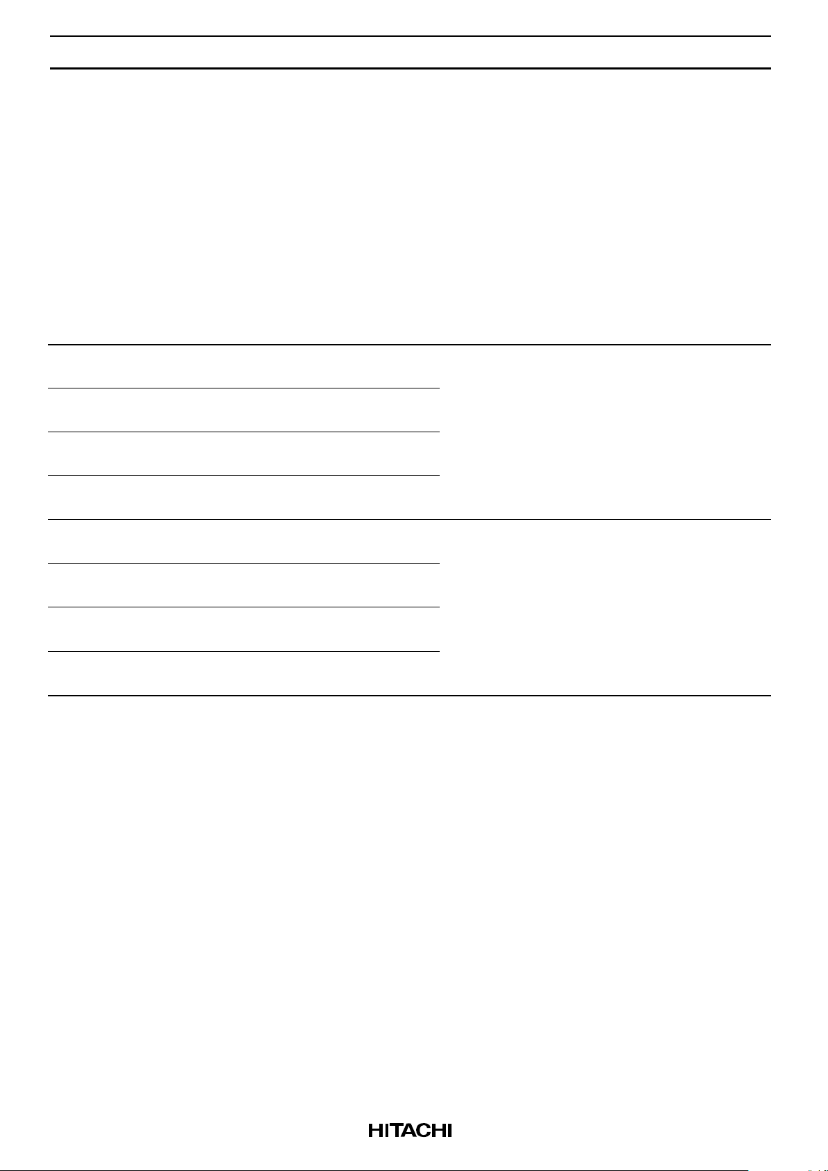
Pin Arrangement (HM5164165 Series)
V
SS
I/O15
I/O14
I/O13
I/O12
V
SS
I/O11
I/O10
I/O9
I/O8
NC
V
SS
LCAS
UCAS
OE
NC
NC
A12
A11
A10
A9
A8
A7
A6
V
SS
1
2
3
4
5
6
7
8
9
10
11
12
13
14
15
16
17
18
19
20
21
22
23
24
25
50
49
48
47
46
45
44
43
42
41
40
39
38
37
36
35
34
33
32
31
30
29
28
27
26
V
CC
I/O0
I/O1
I/O2
I/O3
V
CC
I/O4
I/O5
I/O6
I/O7
NC
V
CC
WE
RAS
NC
NC
NC
NC
A0
A1
A2
A3
A4
A5
V
CC
50-pin TSOP
(Top view)
V
SS
I/O15
I/O14
I/O13
I/O12
V
SS
I/O11
I/O10
I/O9
I/O8
NC
V
SS
LCAS
UCAS
OE
NC
NC
A12
A11
A10
A9
A8
A7
A6
V
SS
VCC
I/O0
I/O1
I/O2
I/O3
V
CC
I/O4
I/O5
I/O6
I/O7
NC
V
CC
WE
RAS
NC
NC
NC
NC
A0
A1
A2
A3
A4
A5
V
CC
50-pin SOJ
(Top view)
50
49
48
47
46
45
44
43
42
41
40
39
38
37
36
35
34
33
32
31
30
29
28
27
26
1
2
3
4
5
6
7
8
9
10
11
12
13
14
15
16
17
18
19
20
21
22
23
24
25
Pin Description
Pin name Function
A0 to A12 Address input
— Row/Refresh address A0 to A12
— Column address A0 to A8
I/O0 to I/O15 Data input/output
RAS Row address strobe
UCAS, LCAS Column address strobe
WE Write enable
OE Output enable
V
CC
Power supply
V
SS
Ground
NC No connection
HM5164165 Series, HM5165165 Series
4
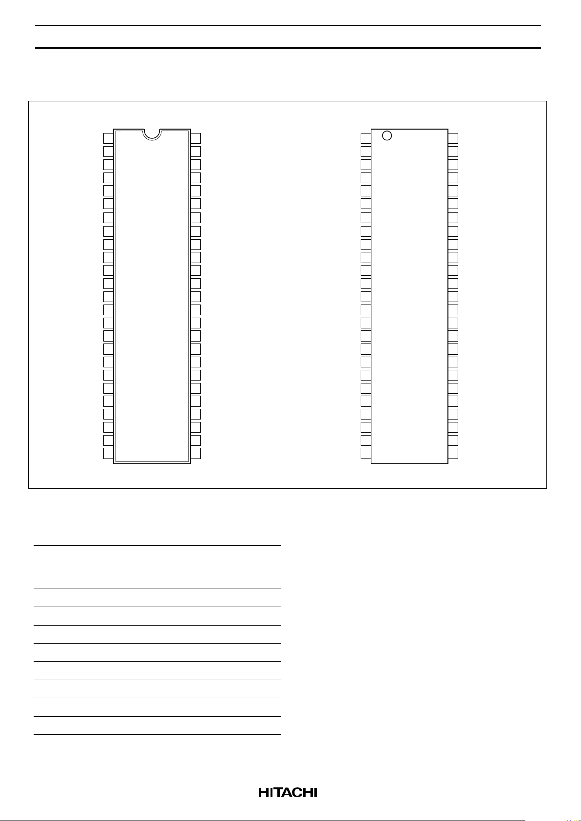
Pin Arrangement (HM5165165 Series)
V
SS
I/O15
I/O14
I/O13
I/O12
V
SS
I/O11
I/O10
I/O9
I/O8
NC
V
SS
LCAS
UCAS
OE
NC
NC
NC
A11
A10
A9
A8
A7
A6
V
SS
1
2
3
4
5
6
7
8
9
10
11
12
13
14
15
16
17
18
19
20
21
22
23
24
25
50
49
48
47
46
45
44
43
42
41
40
39
38
37
36
35
34
33
32
31
30
29
28
27
26
V
CC
I/O0
I/O1
I/O2
I/O3
V
CC
I/O4
I/O5
I/O6
I/O7
NC
V
CC
WE
RAS
NC
NC
NC
NC
A0
A1
A2
A3
A4
A5
V
CC
50-pin TSOP
(Top view)
V
SS
I/O15
I/O14
I/O13
I/O12
V
SS
I/O11
I/O10
I/O9
I/O8
NC
V
SS
LCAS
UCAS
OE
NC
NC
NC
A11
A10
A9
A8
A7
A6
V
SS
VCC
I/O0
I/O1
I/O2
I/O3
V
CC
I/O4
I/O5
I/O6
I/O7
NC
V
CC
WE
RAS
NC
NC
NC
NC
A0
A1
A2
A3
A4
A5
V
CC
50-pin SOJ
(Top view)
50
49
48
47
46
45
44
43
42
41
40
39
38
37
36
35
34
33
32
31
30
29
28
27
26
1
2
3
4
5
6
7
8
9
10
11
12
13
14
15
16
17
18
19
20
21
22
23
24
25
Pin Description
Pin name Function
A0 to A11 Address input
— Row/Refresh address A0 to A11
— Column address A0 to A9
I/O0 to I/O15 Data input/output
RAS Row address strobe
UCAS, LCAS Column address strobe
WE Write enable
OE Output enable
V
CC
Power supply
V
SS
Ground
NC No connection
HM5164165 Series, HM5165165 Series
5
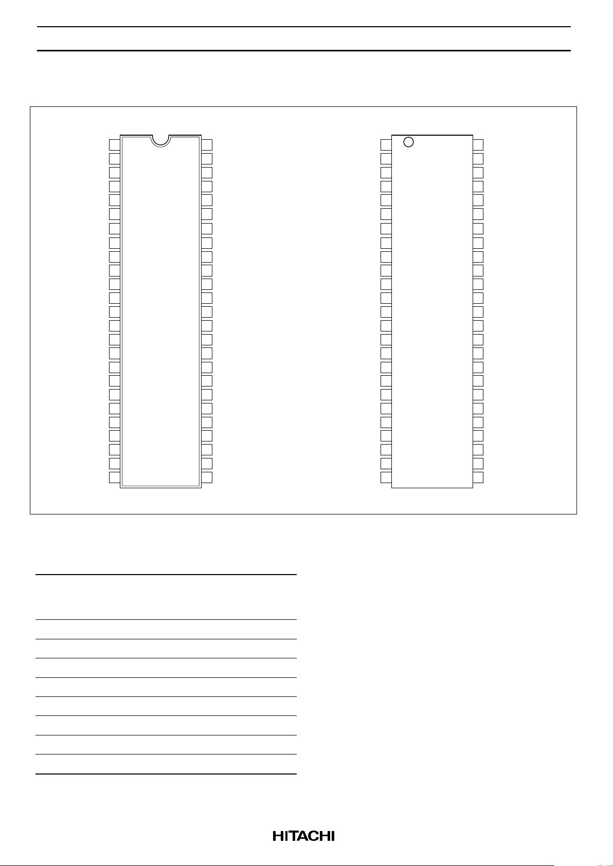
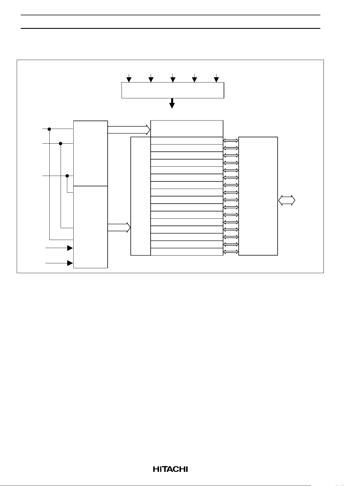
Block Diagram (HM5164165 Series)
•
•
•
•
•
•
A0
A1
to
A8
A9
to
A12
Timing and control
RAS UCAS LCAS WE OE
Column
address
buffers
Row
address
buffers
I/O buffers
I/O0
to
I/O15
Column decoder
Row decoder
4M array
4M array
4M array
4M array
4M array
4M array
4M array
4M array
4M array
4M array
4M array
4M array
4M array
4M array
4M array
4M array
HM5164165 Series, HM5165165 Series
6
Block Diagram (HM5165165 Series)
•
•
•
•
•
•
A0
A1
to
A9
Timing and control
RAS UCAS LCAS WE OE
Column
address
buffers
Row
address
buffers
I/O buffers
I/O0
to
I/O15
Column decoder
Row decoder
4M array
4M array
4M array
4M array
4M array
4M array
4M array
4M array
4M array
4M array
4M array
4M array
4M array
4M array
4M array
4M array
A10
A11
HM5164165 Series, HM5165165 Series
7
Operation Table
RAS LCAS UCAS WE OE I/O 0 to I/O 7 I/O 8 to I/O 15 Operation
H ××××High-Z High-Z Standby
L L H H L Dout High-Z Read cycle
L H L H L High-Z Dout
LLLHLDout Dout
LLHL*
2
×Din × Early write cycle
LHLL*
2
×× Din
LLLL*
2
×Din Din
LLHL*
2
H Din × Delayed write cycle
LHLL*
2
H× Din
LLLL*
2
H Din Din
L L H H to L L to H Dout/Din High-Z Read-modify-write cycle
L H L H to L L to H High-Z Dout/Din
LLLH to LL to HDout/Din Dout/Din
LHH××High-Z High-Z RAS-only refresh cycle
H to L H L H × High-Z High-Z CAS-before-RAS refresh cycle or
H to L L H H × High-Z High-Z Self refresh cycle (L-version)
H to L L L H × High-Z High-Z
L L L H H High-Z High-Z Read cycle (Output disabled)
Notes: 1. H: VIH (inactive) L: VIL (active) ×: VIH or V
IL
2. t
WCS
≥ 0 ns: Early write cycle
t
WCS
< 0 ns: Delayed write cycle
3. Mode is determined by the OR function of the UCAS and LCAS. (Mode is set by the earliest of
UCAS and LCAS active edge and reset by the latest of UCAS and LCAS inactive edge.) However
write operation and output High-Z control are done independently by each UCAS, LCAS.
ex. if RAS = H to L, LCAS = L, UCAS = H, then CAS-before-RAS refresh cycle is selected.
HM5164165 Series, HM5165165 Series
8
Absolute Maximum Ratings
Parameter Symbol Value Unit
Terminal voltage on any pin relative to V
SS
V
T
–0.5 to VCC + 0.5 ( 4.6 V (max)) V
Power supply voltage relative to V
SS
V
CC
–0.5 to +4.6 V
Short circuit output current Iout 50 mA
Power dissipation P
T
1.0 W
Storage temperature Tstg –55 to +125 °C
DC Operating Conditions
Parameter Symbol Min Typ Max Unit Notes
Supply voltage V
CC
3.0 3.3 3.6 V 1, 2
V
SS
000 V2
Input high voltage V
IH
2.0 — VCC + 0.3 V 1
Input low voltage V
IL
–0.3 — 0.8 V 1
Ambient temperature range Ta 0 — 70 ˚C
Notes: 1. All voltage referred to VSS.
2. The supply voltage with all V
CC
pins must be on the same level. The supply voltage with all VSS pins
must be on the same level.

HM5164165 Series, HM5165165 Series
9
DC Characteristics (HM5164165 Series)
HM5164165
-5 -6
Parameter Symbol Min Max Min Max Unit Test conditions
Operating current*
1, *2
I
CC1
— 120 — 110 mA tRC = min
Standby current I
CC2
— 2 — 2 mA TTL interface
RAS, UCAS, LCAS = V
IH
Dout = High-Z
— 0.5 — 0.5 mA CMOS interface
RAS, UCAS,
LCAS V
CC
– 0.2 V
Dout = High-Z
Standby current
(L-version)
I
CC2
— 150 — 150 µA CMOS interface
RAS, UCAS,
LCAS V
CC
– 0.2 V
Dout = High-Z
RAS-only refresh current*
2
I
CC3
— 120 — 110 mA tRC = min
Standby current*
1
I
CC5
—5 —5 mARAS = V
IH
UCAS, LCAS = V
IL
Dout = enable
CAS-before-RAS refresh
current
I
CC6
— 120 — 110 mA tRC = min
EDO page mode current*
1, *3
I
CC7
— 120 — 110 mA RAS = VIL , CAS cycle,
t
HPC
= t
HPC
min
Battery backup current*
4
(Standby with CBR refresh)
(L-version)
I
CC10
— 500 — 500 µA CMOS interface
Dout = High-Z
CBR refresh: t
RC
= 31.3 µs
t
RAS
0.3 µs
Self refresh mode current
(L-version)
I
CC11
— 400 — 400 µA CMOS interface
RAS, UCAS, LCAS 0.2 V
Dout = High-Z
Input leakage current I
LI
–5 5 –5 5 µA 0 V Vin VCC + 0.3 V
Output leakage current I
LO
–5 5 –5 5 µA 0 V Vout V
CC
Dout = disable
Output high voltage V
OH
2.4 V
CC
2.4 V
CC
V High Iout = –2 mA
Output low voltage V
OL
0 0.4 0 0.4 V Low Iout = 2 mA
Notes: 1. ICC depends on output load condition when the device is selected. ICC max is specified at the output
open condition.
2. Address can be changed once or less while RAS = V
IL
.
3. Measured with one sequential address change per EDO cycle, t
HPC
.
4. V
IH
VCC – 0.2 V, 0 V VIL 0.2 V.

HM5164165 Series, HM5165165 Series
10
DC Characteristics (HM5165165 Series)
HM5165165
-5 -6
Parameter Symbol Min Max Min Max Unit Test conditions
Operating current*
1, *2
I
CC1
— 140 — 120 mA tRC = min
Standby current I
CC2
— 2 — 2 mA TTL interface
RAS, UCAS, LCAS = V
IH
Dout = High-Z
— 0.5 — 0.5 mA CMOS interface
RAS, UCAS,
LCAS V
CC
– 0.2 V
Dout = High-Z
Standby current
(L-version)
I
CC2
— 150 — 150 µA CMOS interface
RAS, UCAS,
LCAS V
CC
– 0.2 V
Dout = High-Z
RAS-only refresh current*
2
I
CC3
— 140 — 120 mA tRC = min
Standby current*
1
I
CC5
—5 —5 mARAS = V
IH
UCAS, LCAS = V
IL
Dout = enable
CAS-before-RAS refresh
current
I
CC6
— 140 — 120 mA tRC = min
EDO page mode current*
1, *3
I
CC7
— 120 — 110 mA RAS = VIL , CAS cycle,
t
HPC
= t
HPC
min
Battery backup current*
4
(Standby with CBR refresh)
(L-version)
I
CC10
— 500 — 500 µA CMOS interface
Dout = High-Z
CBR refresh: t
RC
= 31.3 µs
t
RAS
0.3 µs
Self refresh mode current
(L-version)
I
CC11
— 400 — 400 µA CMOS interface
RAS, UCAS, LCAS 0.2 V
Dout = High-Z
Input leakage current I
LI
–5 5 –5 5 µA 0 V Vin VCC + 0.3 V
Output leakage current I
LO
–5 5 –5 5 µA 0 V Vout V
CC
Dout = disable
Output high voltage V
OH
2.4 V
CC
2.4 V
CC
V High Iout = –2 mA
Output low voltage V
OL
0 0.4 0 0.4 V Low Iout = 2 mA
Notes: 1. ICC depends on output load condition when the device is selected. ICC max is specified at the output
open condition.
2. Address can be changed once or less while RAS = V
IL
.
3. Measured with one sequential address change per EDO cycle, t
HPC
.
4. V
IH
VCC – 0.2 V, 0 V VIL 0.2 V.

HM5164165 Series, HM5165165 Series
11
Capacitance (Ta = 25°C, VCC = 3.3 V ± 0.3 V)
Parameter Symbol Min Typ Max Unit Notes
Input capacitance (Address) C
I1
——5 pF1
Input capacitance (Clocks) C
I2
——7 pF1
Output capacitance (Data-in, Data-out) C
I/O
— — 7 pF 1, 2
Notes : 1. Capacitance measured with Boonton Meter or effective capacitance measuring method.
2. RAS, UCAS and LCAS = V
IH
to disable Dout.

HM5164165 Series, HM5165165 Series
12
AC Characteristics (Ta = 0 to +70°C, VCC = 3.3 V ± 0.3 V, VSS = 0 V)*
1, *2, *19, *27
Test Conditions
• Input rise and fall time: 2 ns
• Input pulse levels: VIL = 0 V, VIH = 3.0 V
• Input timing reference levels: 0.8 V, 2.0 V
• Output timing reference levels: 0.8 V, 2.0 V
• Output load: 1 TTL gate + CL (100 pF) (Including scope and jig)
Read, Write, Read-Modify-Write and Refresh Cycles (Common parameters)
HM5164165/HM5165165
-5 -6
Parameter Symbol Min Max Min Max Unit Notes
Random read or write cycle time t
RC
84 — 104 — ns
RAS precharge time t
RP
30 — 40 — ns
CAS precharge time t
CP
8 — 10 — ns 31
RAS pulse width t
RAS
50 10000 60 10000 ns
CAS pulse width t
CAS
8 10000 10 10000 ns
Row address setup time t
ASR
0—0—ns
Row address hold time t
RAH
8 — 10 — ns
Column address setup time t
ASC
0 — 0 — ns 28
Column address hold time t
CAH
8 — 10 — ns 28
RAS to CAS delay time t
RCD
12 37 14 45 ns 3
RAS to column address delay time t
RAD
10 25 12 30 ns 4
RAS hold time t
RSH
13 — 15 — ns
CAS hold time t
CSH
35 — 40 — ns
CAS to RAS precharge time t
CRP
5 — 5 — ns 29
OE to Din delay time t
OED
13 — 15 — ns 5
OE delay time from Din t
DZO
0 — 0 — ns 6
CAS delay time from Din t
DZC
0 — 0 — ns 6
Transition time (rise and fall) t
T
2 50 2 50 ns 7
HM5164165 Series, HM5165165 Series
13
Read Cycle
HM5164165/HM5165165
-5 -6
Parameter Symbol Min Max Min Max Unit Notes
Access time from RAS t
RAC
— 50 — 60 ns 8, 9
Access time from CAS t
CAC
— 13 — 15 ns 9, 10, 17
Access time from address t
AA
— 25 — 30 ns 9, 11, 17
Access time from OE t
OEA
— 13 — 15 ns 9
Read command setup time t
RCS
0 — 0 — ns 28
Read command hold time to CAS t
RCH
0 — 0 — ns 12, 29
Read command hold time from RAS t
RCHR
50 — 60 — ns
Read command hold time to RAS t
RRH
0 — 0 — ns 12
Column address to RAS lead time t
RAL
25 — 30 — ns
Column address to CAS lead time t
CAL
15 — 18 — ns
CAS to output in low-Z t
CLZ
0—0—ns
Output data hold time t
OH
3 — 3 — ns 21
Output data hold time from OE t
OHO
3—3—ns
Output buffer turn-off time t
OFF
— 13 — 15 ns 13, 21
Output buffer turn-off to OE t
OEZ
— 13 — 15 ns 13
CAS to Din delay time t
CDD
13 — 15 — ns 5
Output data hold time from RAS t
OHR
3 — 3 — ns 21
Output buffer turn-off to RAS t
OFR
— 13 — 15 ns 13, 21
Output buffer turn-off to WE t
WEZ
— 13 — 15 ns 13
WE to Din delay time t
WED
13 — 15 — ns
RAS to Din delay time t
RDD
13 — 15 — ns

HM5164165 Series, HM5165165 Series
14
Write Cycle
HM5164165/HM5165165
-5 -6
Parameter Symbol Min Max Min Max Unit Notes
Write command setup time t
WCS
0 — 0 — ns 14, 28
Write command hold time t
WCH
8 — 10 — ns 28
Write command pulse width t
WP
8 — 10 — ns
Write command to RAS lead time t
RWL
13 — 15 — ns
Write command to CAS lead time t
CWL
8 — 10 — ns 30
Data-in setup time t
DS
0 — 0 — ns 15, 30
Data-in hold time t
DH
8 — 10 — ns 15, 30
Read-Modify-Write Cycle
HM5164165/HM5165165
-5 -6
Parameter Symbol Min Max Min Max Unit Notes
Read-modify-write cycle time t
RWC
116 — 140 — ns
RAS to WE delay time t
RWD
67 — 79 — ns 14
CAS to WE delay time t
CWD
30 — 34 — ns 14
Column address to WE delay time t
AWD
42 — 49 — ns 14
OE hold time from WE t
OEH
13 — 15 — ns
Refresh Cycle
HM5164165/HM5165165
-5 -6
Parameter Symbol Min Max Min Max Unit Notes
CAS setup time (CBR refresh cycle) t
CSR
5 — 5 — ns 28
CAS hold time (CBR refresh cycle) t
CHR
8 — 10 — ns 29
WE setup time (CBR refresh cycle) t
WRP
0—0—ns
WE hold time (CBR refresh cycle) t
WRH
8 — 10 — ns
RAS precharge to CAS hold time t
RPC
5 — 5 — ns 28

HM5164165 Series, HM5165165 Series
15
EDO Page Mode Cycle
HM5164165/HM5165165
-5 -6
Parameter Symbol Min Max Min Max Unit Notes
EDO page mode cycle time t
HPC
20 — 25 — ns 20
EDO page mode RAS pulse width t
RASP
— 100000 — 100000 ns 16
Access time from CAS precharge t
CPA
— 28 — 35 ns 9, 17, 29
RAS hold time from CAS precharge t
CPRH
28 — 35 — ns
Output data hold time from CAS low t
DOH
3 — 3 — ns 9, 22
CAS hold time referred OE t
COL
8 — 10 — ns
CAS to OE setup time t
COP
5—5—ns
Read command hold time from
CAS precharge
t
RCHC
28 — 35 — ns
Write pulse width during CAS precharge t
WPE
8 — 10 — ns
OE precharge time t
OEP
8 — 10 — ns
EDO Page Mode Read-Modify-Write Cycle
HM5164165/HM5165165
-5 -6
Parameter Symbol Min Max Min Max Unit Notes
EDO page mode read-modify-write cycle
time
t
HPRWC
57 — 68 — ns
WE delay time from CAS precharge t
CPW
45 — 54 — ns 14, 29
Refresh (HM5164165 Series)
Parameter Symbol Max Unit Note
Refresh period t
REF
64 ms 8192 cycles
Refresh period (L-version) t
REF
128 ms 8192 cycles

HM5164165 Series, HM5165165 Series
16
Refresh (HM5165165 Series)
Parameter Symbol Max Unit Note
Refresh period t
REF
64 ms 4096 cycles
Refresh period (L-version) t
REF
128 ms 4096 cycles
Self Refresh Mode (L-version)
HM5164165L/HM5165165L
-5 -6
Parameter Symbol Min Max Min Max Unit Notes
RAS pulse width (self refresh) t
RASS
100 — 100 — µs 26
RAS precharge time (self refresh) t
RPS
90 — 110 — ns 26
CAS hold time (self refresh) t
CHS
–50 — –50 — ns 30
Notes: 1. AC measurements assume tT = 2 ns.
2. An initial pause of 200 µs is required after power up followed by a minimum of eight initialization
cycles (any combination of cycles containing RAS-only refresh or CAS-before-RAS refresh).
3. Operation with the t
RCD
(max) limit insures that t
RAC
(max) can be met, t
RCD
(max) is specified as a
reference point only; if t
RCD
is greater than the specified t
RCD
(max) limit, than the access time is
controlled exclusively by t
CAC
.
4. Operation with the t
RAD
(max) limit insures that t
RAC
(max) can be met, t
RAD
(max) is specified as a
reference point only; if t
RAD
is greater than the specified t
RAD
(max) limit, then access time is
controlled exclusively by t
AA
.
5. Either t
OED
or t
CDD
must be satisfied.
6. Either t
DZO
or t
DZC
must be satisfied.
7. V
IH
(min) and VIL (max) are reference levels for measuring timing of input signals. Also, transition
times are measured between V
IH
(min) and VIL (max).
8. Assumes that t
RCD
t
RCD
(max) and t
RAD
t
RAD
(max). If t
RCD
or t
RAD
is greater than the maximum
recommended value shown in this table, t
RAC
exceeds the value shown.
9. Measured with a load circuit equivalent to 1 TTL loads and 100 pF.
10.Assumes that t
RCD
t
RCD
(max) and t
RCD
+ t
CAC
(max) t
RAD
+ tAA (max).
11.Assumes that t
RAD
t
RAD
(max) and t
RCD
+ t
CAC
(max) t
RAD
+ tAA (max).
12.Either t
RCH
or t
RRH
must be satisfied for a read cycles.
13.t
OFF
(max), t
OEZ
(max), t
WEZ
(max) and t
OFR
(max) define the time at which the outputs achieve the
open circuit condition and are not referred to output voltage levels.
14.t
WCS
, t
RWD
, t
CWD
, t
AWD
and t
CPW
are not restrictive operating parameters. They are included in the data
sheet as electrical characteristics only; if t
WCS
t
WCS
(min), the cycle is an early write cycle and the
data out pin will remain open circuit (high impedance) throughout the entire cycle; if t
RWD
t
RWD
(min), t
CWD
t
CWD
(min), and t
AWD
t
AWD
(min), or t
CWD
t
CWD
(min), t
AWD
t
AWD
(min) and t
CPW
t
CPW
(min), the cycle is a read-modify-write and the data output will contain data read from the selected
cell; if neither of the above sets of conditions is satisfied, the condition of the data out (at access
time) is indeterminate.
15.t
DS
and tDH are referred to UCAS and LCAS leading edge in early write cycles and to WE leading
edge in delayed write or read-modify-write cycles.

HM5164165 Series, HM5165165 Series
17
16.t
RASP
defines RAS pulse width in EDO page mode cycles.
17.Access time is determined by the longest among t
AA
, t
CAC
and t
CPA
.
18.In delayed write or read-modify-write cycles, OE must disable output buffer prior to applying data to
the device.
19.When output buffers are enabled once, sustain the low impedance state until valid data is obtained.
When output buffer is turned on and off within a very short time, generally it causes large V
CC/VSS
line noise, which causes to degrade VIH min/VIL max level.
20.t
HPC
(min) can be achieved during a series of EDO page mode write cycles or EDO page mode read
cycles. If both write and read operation are mixed in a EDO page mode RAS cycle (EDO page
mode mix cycle (1), (2)), minimum value of CAS cycle (t
CAS
+ tCP + 2 tT) becomes greater than the
specified t
HPC
(min) value.The value of CAS cycle time of mixed EDO page mode is shown in EDO
page mode mix cycle (1) and (2).
21.Data output turns off and becomes high impedance from later rising edge of RAS and CAS. Hold
time and turn off time are specified by the timing specifications of later rising edge of RAS and CAS
between t
OHR
and tOH, and between t
OFR
and t
OFF
.
22.t
DOH
defines the time at which the output level go cross. VOL = 0.8 V, VOH = 2.0 V of output timing
reference level.
23.Before and after self refresh mode, execute CBR refresh to all refresh addresses in or within 64 ms
period on the condition a and b below.
a. Enter self refresh mode within 15.6 µs after either burst refresh or distributed refresh at equal
interval to all refresh addresses are completed.
b. Start burst refresh or distributed refresh at equal interval to all refresh addresses within
15.6µs after exiting from self refresh mode.
24.In case of entering from RAS-only-refresh, it is necessary to execute CBR refresh before and after
self refresh mode according as note 23.
25.For L-version, it is available to apply each 128 ms and 31.2 µs instead of 64 ms and 15.6 µs at
note 23.
26 At t
RASS
> 100 µs, self refresh mode is activated, and not activated at t
RASS
< 10 µs. It is undefined
within the range of 10 µs t
RASS
100 µs. For t
RASS
10 µs, it is necessary to satisfy t
RPS
.
27.When both UCAS and LCAS go low at the same time, all 16-bit data are written into the device.
UCAS and LCAS cannot be staggered within the same write/read cycles.
28.t
ASC
, t
CAH
, t
RCS
, t
WCS
, t
WCH
, t
CSR
and t
RPC
are determined by the earlier falling edge of UCAS or LCAS.
29.t
CRP
, t
CHR
, t
RCH
, t
CPA
and t
CPW
are determined by the later rising edge of UCAS or LCAS.
30.t
CWL
, tDH, tDS and t
CHS
should be satisfied by both UCAS and LCAS.
31.t
CP
is determined by the time that both UCAS and LCAS are high.
32.XXX: H or L (H: V
IH
(min) VIN VIH (max), L: VIL (min) VIN VIL (max))
///////: Invalid Dout
When the address, clock and input pins are not described on timing waveforms, their pins must be
applied V
IH
or VIL.

HM5164165 Series, HM5165165 Series
18
Notes concerning 2CAS control
Please do not separate the UCAS/LCAS operation timing intentionally. However skew between
UCAS/LCAS are allowed under the following conditions.
1. Each of the UCAS/LCAS should satisfy the timing specifications individually.
2. Different operation mode for upper/lower byte is not allowed; such as following.
RAS
UCAS
LCAS
WE
Delayed write
Early write
3. Closely separated upper/lower byte control is not allowed. However when the condition (t
CP
≤ tUL) is
satisfied, EDO page mode can be performed.
RAS
UCAS
LCAS
t
UL
4. Byte control operation by remaining UCAS or LCAS high is guaranteed.

HM5164165 Series, HM5165165 Series
19
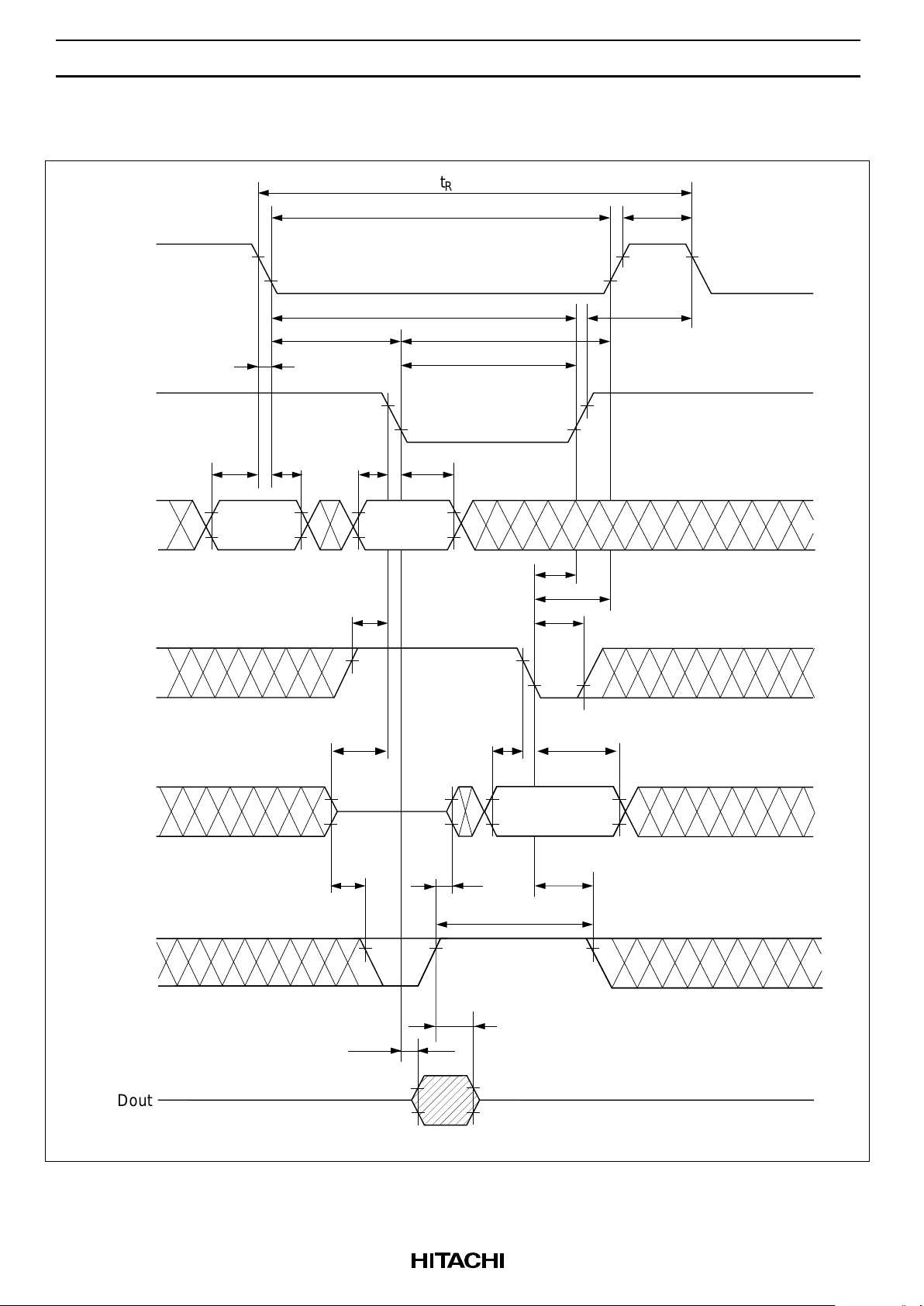
Timing Waveforms*
32
Read Cycle
RAS
Address
WE
Dout
OE
Din
t
RC
Row
Column
t
RCS
t
RCH
t
CDD
t
DZC
High-Z
Dout
t
DZO
t
OED
t
RAC
t
OEA
t
AA
t
CAC
t
CLZ
t
OH
t
OFF
t
OHO
t
OEZ
UCAS
LCAS
t
RDD
t
WED
t
OFR
t
OHR
t
WEZ
t
RAS
t
CAS
t
RP
t
CSH
t
RCD
t
RSH
t
CRP
t
T
t
RAD
t
RAL
t
CAL
t
ASR t
ASC
t
CAH
t
RCHR
t
RRH
t
RAH

HM5164165 Series, HM5165165 Series
20
Early Write Cycle
RAS
Address
WE
Din
Dout
t
RC
*
t
RAS
t
RP
t
CRP
t
CSH
t
RCD
t
RSH
t
CAS
t
T
t
ASRtRAH
t
ASC
t
CAH
ColumnRow
t
WCS
t
WCH
t
DS
t
DH
Din
t
WCS WCS
(min)
High-Z*
t
UCAS
LCAS
HM5164165 Series, HM5165165 Series
21
Delayed Write Cycle*
18
Address
UCAS
LCAS
RAS
WE
Din
OE
Dout
t
RC
t
RAS
t
RP
t
CSH
t
RCD
t
RSH
t
CAS
t
CRP
t
T
ColumnRow
t
ASR
t
RAH
t
ASC t
CAH
t
RCS
t
CWL
t
RWL
t
WP
t
DZC
t
DS
t
DH
t
DZO
t
OED
t
OEH
t
OEP
t
CLZ
t
OEZ
High-Z
Invalid Dout
Din
High-Z

HM5164165 Series, HM5165165 Series
22
Read-Modify-Write Cycle*
18
Address
RAS
Din
Dout
OE
WE
t
RWC
t
RAS
t
RP
t
CRP
t
CAS
t
RCD
t
T
t
RAD
t
ASR
t
RAH
t
ASC
t
CAH
ColumnRow
t
RCS
t
CWD
t
CWL
t
AWD
t
RWD
t
RWL
t
WP
t
DZC t
DH
t
DS
Din
High-Z
t
DZO
t
OED
t
OEH
t
OEA
t
CAC
t
AA
t
RAC
t
OHO
t
OEZ
t
CLZ
Dout
High-Z
UCAS
LCAS
t
OEP

HM5164165 Series, HM5165165 Series
23
RAS-Only Refresh Cycle
RAS
UCAS
LCAS
Address
Dout
High-Z
Row
t
RC
t
RP
t
RAS
t
T
t
CRP
t
RPC
t
CRP
t
ASR
t
RAH
t
OFF
t
OFR

HM5164165 Series, HM5165165 Series
24
CAS-Before-RAS Refresh Cycle
RAS
UCAS
LCAS
WE
Address
Dout
High-Z
t
OFF
t
OFR
t
WRPtWRH
t
WRPtWRH
t
CP
t
RPC
t
CSR
t
CHR
t
CP
t
RPC
t
CSR
t
CHR
t
CRP
t
RP
t
RAS
t
RC
t
RC
t
RP
t
RAS
t
RP
t
T

HM5164165 Series, HM5165165 Series
25
Hidden Refresh Cycle
Din
OE
Dout
WE
Address
RAS
t
RC
t
RC
t
RC
t
RP
t
RAS
t
RP
t
RAS
t
RP
t
RAS
t
T
t
RCD
t
RSH
t
CHR
t
CRP
t
RAD
t
RAL
t
CAH
t
ASC
t
RAH
t
ASR
t
CDD
t
DZC
t
OED
t
OEZ
t
OHO
t
OFF
t
OH
t
CAC
t
AA
t
RAC
t
CLZ
Dout
ColumnRow
t
OEA
High-Z
t
RCH
t
RRH
UCAS
LCAS
t
WED
t
RDD
t
WEZ
t
OFR
t
OHR
t
RCS
t
DZO
HM5164165 Series, HM5165165 Series
26
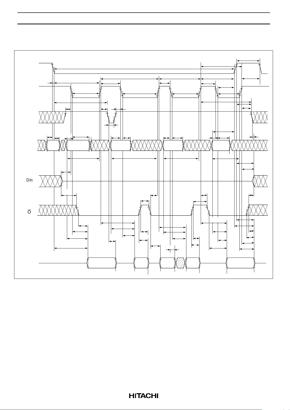
EDO Page Mode Read Cycle
Din
OE
Dout
WE
Address
RAS
UCAS
LCAS
t
CP
t
CP
t
CP
t
T
t
RCH
t
RRH
t
DZC
t
CDD
t
RDD
High-Z
t
OFR
t
OEZ
t
OHO
t
OFF
t
OH
t
OHR
t
t
COL
t
OEP
t
t
CPA
t
AA
t
CAC
t
CAC
t
OEA
t
AA
t
RAC
t
AA
t
CAC
t
CPA
t
t
OEZ
t
OEA
t
OEZ
t
AA
t
CAC
t
t
RASP
COP
t
RP
t
CAS
t
CAS
t
CAS
t
CAL
t
CSH
t
HPC
t
HPC
CRP
t
t
ASR
t
RAH
Column 1 Column 2 Column 3
Column 4
t
t
CAH
t
ASC
t
CAH
t
CAH
t
ASC
t
CAH
t
ASC
t
WED
t
RAL
Row
Dout 2 Dout 2 Dout 4
Dout 1
t
CAS
t
RCS
t
t
WPE
Dout 3
t
OHO
t
t
CPRH
t
HPC
t
OEA
t
WEZ
DZO
t
OED
t
OEP
OHO
DOH
RCH
t
RCS
t
RCHR
t
CAL
t
CAL
t
CAL
t
RSH
t
RCHC
CPA
ASC
HM5164165 Series, HM5165165 Series
27
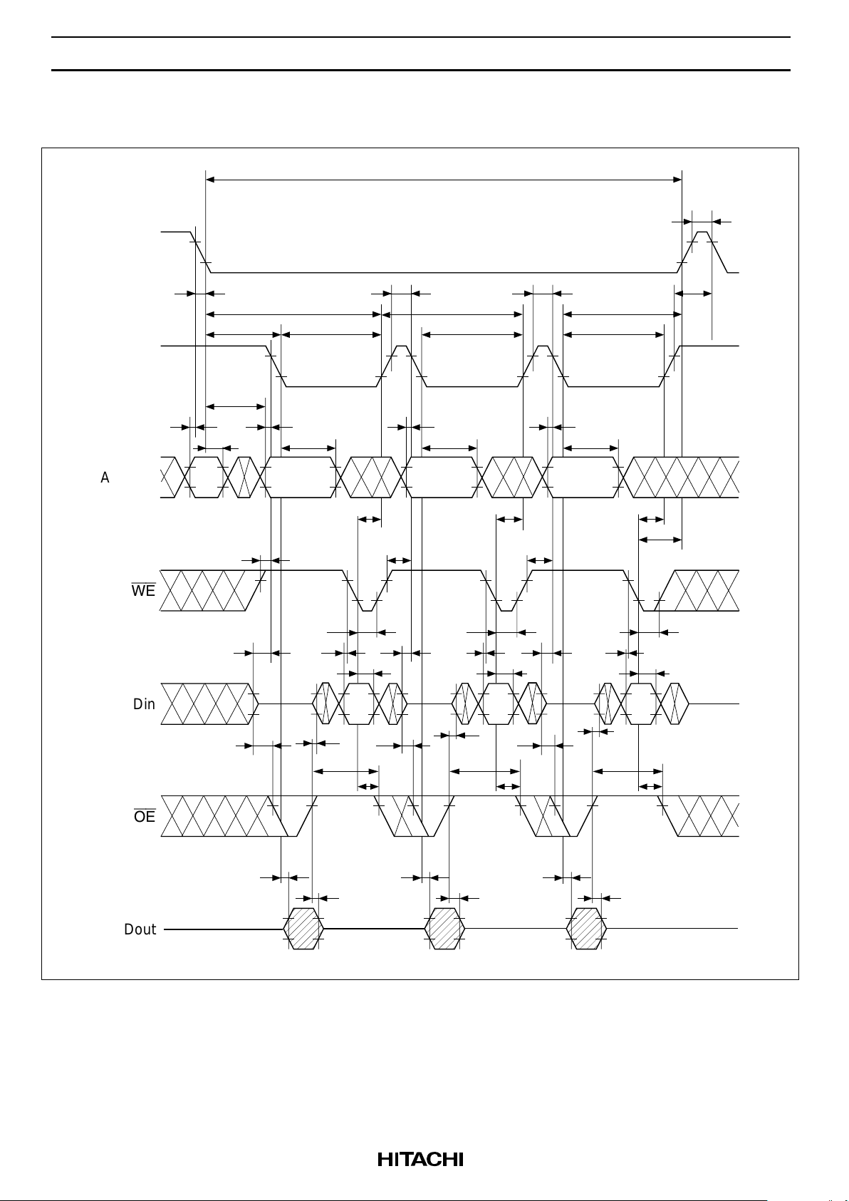
EDO Page Mode Read Cycle (2CAS control)
OE
WE
Address
t
DZC
t
CDD
t
RDD
High-Z
t
OFR
t
OEZ
t
OHO
t
OFF
t
OH
t
OHR
t
t
COL
t
t
CPA
t
AA
t
CAC
t
CAC
t
OEA
t
AA
t
RAC
t
AA
t
DOH
t
t
OEZ
t
t
OEZ
t
AA
t
CAC
t
COP
t
OEP
t
ASR
t
RAH
Column 1 Column 2 Column 3
Column 4
t
t
CAH
t
ASC
t
CAH
t
CAH
t
ASC
t
CAH
t
ASC
t
WED
t
RAL
Row
Dout 2 Dout 4
Dout 1
t
RCS
t
OHO
t
OEA
DZO
t
OED
t
OEP
t
CAC
t
RCHC
CPA
ASC
RAS
UCAS
LCAS
t
CP
t
CP
t
CP
t
T
t
RCH
t
RRH
t
RASP
t
RP
t
CAS
t
CAS
t
CAS
t
CSH
t
HPC
t
HPC
t
HPC
CRP
t
t
CAS
t
RSH
L Dout
U Dout
Dout 1
Dout 3
Dout 2
OHO
OEA
Dout 4
t
CPA
t
CAL CAL CAL
t t
CAL
t
Din
HM5164165 Series, HM5165165 Series
28
EDO Page Mode Early Write Cycle
*
t
WCS WCS
(min)
RAS
Address
WE
Din
Dout
t
RASP
t
RP
t
T
t
CSH
t
HPC
t
RSH
t
CRP
t
CAS
t
CP
t
CAS
t
CP
t
CAS
t
RCD
t
ASR
t
RAH
t
ASCtCAH
t
ASC
t
CAH
t
ASC
t
CAH
t
WCH
t
WCS
t
WCH
t
WCS
t
WCH
t
WCS
t
DH
t
DS
t
DH
t
DS
t
DH
t
DS
Din 1 Din 2 Din N
High-Z*
t
Row Column 1 Column 2 Column N
UCAS
LCAS
HM5164165 Series, HM5165165 Series
29
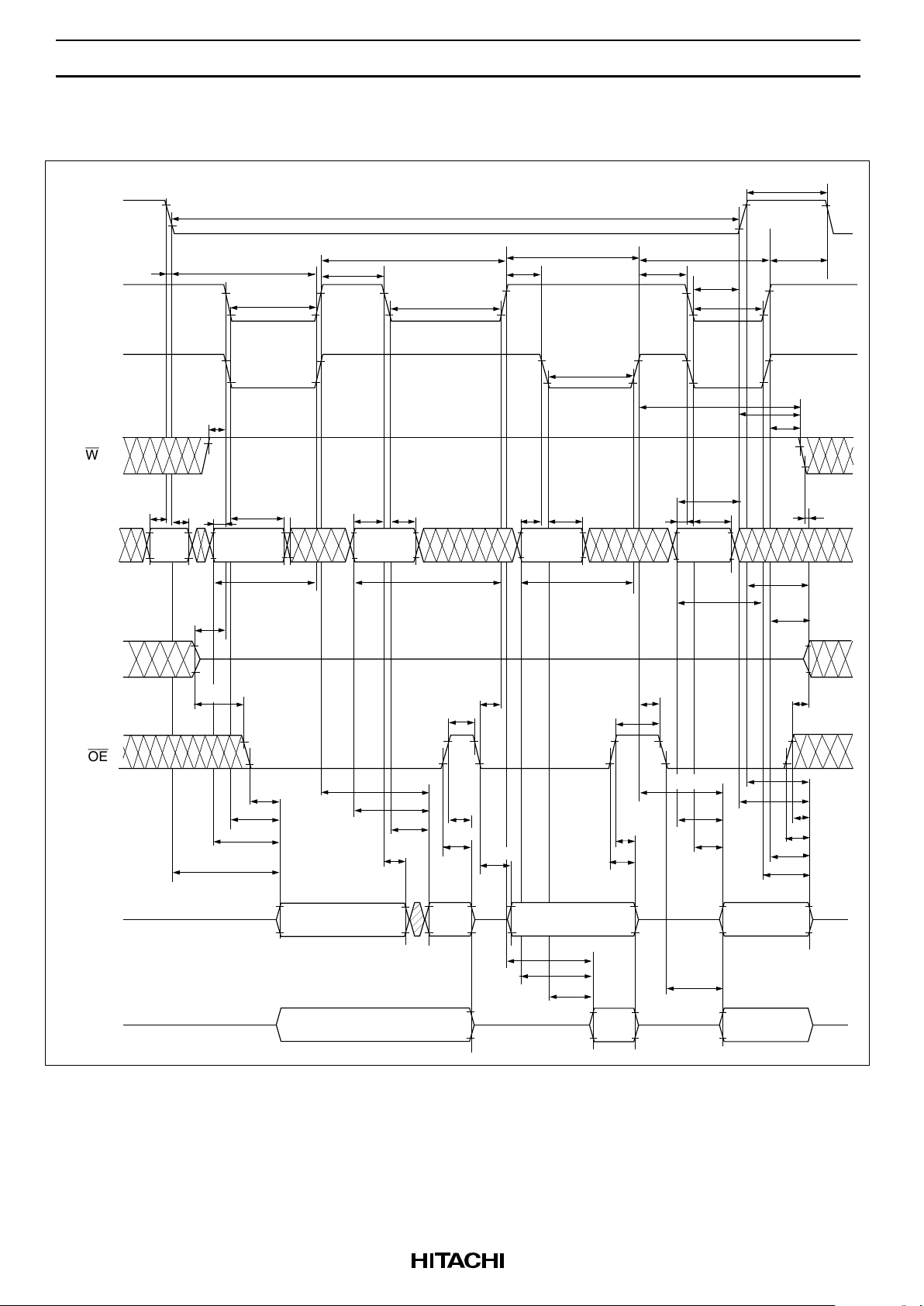
EDO Page Mode Delayed Write Cycle*
18
WE
Din
OE
Dout
Address
RAS
t
RASP
t
RP
t
CRP
t
RSH
t
CAS
t
HPC
t
CAS
t
CAS
t
CSH
t
RCD
t
T
t
CP
t
CP
t
ASC
t
CAH
t
ASC
t
CAH
t
ASC
t
CAH
t
RAD
t
ASR
t
RAH
t
RCS
t
RCS
t
RCS
t
RWL
t
CWL
t
CWL
t
CWL
t
WP
t
WP
t
WP
t
DZCtDS
t
DZCtDS
t
DSt
DZC
t
DH
t
DH
t
DH
t
DZO
t
OED
t
DZO
t
OED
t
DZO
t
OED
t
OEH
t
OEH
t
OEH
t
OEZ
t
CLZ
t
CLZ
t
OEZ
t
CLZ
t
OEZ
Invalid Dout Invalid Dout Invalid Dout
Din
1
Din
2
Din
N
Column NColumn 2Column 1Row
High-Z
UCAS
LCAS
t
OEP
t
OEP
t
OEP

HM5164165 Series, HM5165165 Series
30
EDO Page Mode Read-Modify-Write Cycle*
18
WE
Din
OE
Dout
Address
RAS
t
RASP
t
CRP
t
CP
t
HPRWC
t
T
t
RCD
t
CAS
t
CP
t
CAS
t
CAS
t
RAD
t
ASR
t
ASC
t
ASC
t
ASC
t
RAH
t
CAH
t
CAH
t
CAH
t
CWL
t
CPW
t
CWL
t
CPW
t
CWL
t
RWD
t
AWD
t
AWD
t
AWD
t
CWD
t
RCS
t
CWD
t
RCS
t
CWD
t
RCS
t
WP
t
WP
t
WP
t
DSt
DZC
t
DSt
DZC
t
DSt
DZC
t
DH
t
DH
t
DH
t
DZO
t
DZO
t
DZO
t
OEH
t
OEP
t
OEP
t
OEP
t
OEH
t
OEH
t
AA
t
RAC
t
OEZ
t
CLZ
Dout NDout 2Dout 1
Din
1
Din
2
Din
N
Column NColumn 2Column 1
t
RP
Row
t
RWL
t
OHO
t
OEA
t
CAC
t
OEZ
t
CLZ
t
OHO
t
OEA
t
CAC
t
CPA
t
OEZ
t
CLZ
t
OHO
t
OEA
t
CAC
t
CPA
High-Z
t
OED
t
OED
t
OED
AA
t
AA
t
t
RSH
UCAS
LCAS

HM5164165 Series, HM5165165 Series
31
EDO Page Mode Mix Cycle (1) *
20
OE
Dout
WE
Address
RAS
UCAS
LCAS
t
CP
t
CP
t
CP
t
T
t
RCH
t
RRH
t
CDD
t
RDD
High-Z
t
OFR
t
OEZ
t
OHO
t
OFF
t
OH
t
CPA
t
AA
t
CAC
t
AA
t
CAC
t
CPA
t
OEZ
t
AA
t
OEA
t
t
RASP
t
RP
t
CAS
t
CAS
t
CAS
CRP
t
t
ASR
t
RAH
Column 1 Column 2 Column 3 Column 4
t
ASC
t
CAH
t
ASC
t
CAH
t
CAH
t
CAH
t
RAL
t
CAL
Row
Dout 2 Dout 4
CPA
t
CAS
t
WCS
Dout 3
t
t
t
WP
t
WCH
t
WED
t
WEZ
t
DS
t
DH
t
DS
t
DH
Din 3Din 1
t
OEA
t
OED
t
OEP
t
CAC
t
ASC
t
CPW
t
AWD
OHO
t
CAL
t
RCS
t
RCS
t
CSH
t
RCD
t
RSH
DOH
ASC
t
Din

HM5164165 Series, HM5165165 Series
32
EDO Page Mode Mix Cycle (2)*
20
Din
OE
Dout
WE
Address
RAS
UCAS
LCAS
t
CP
t
CP
t
CP
t
T
t
RCH
t
RRH
t
CDD
t
RDD
High-Z
t
OFR
t
OEZ
t
OHO
t
OFF
t
OH
t
CPA
t
AA
t
CAC
t
AA
t
CAC
t
OEZ
t
t
OEA
t
t
RASP
t
RP
t
CAS
t
CAS
t
CAS
t
CSH
CRP
t
t
ASR
t
RAH
Column 1 Column 2 Column 3 Column 4
t
ASC
t
CAH
t
ASC
t
CAH
t
CAH
t
ASC
t
CAH
t
RAL
t
RCS
Row
Dout 1 Dout 4
CPA
t
CAS
Dout 3
t
OHO
t
WED
t
WEZ
t
DS
t
DH
t
DS
t
Din 3Din 2
t
OEA
t
t
CAC
t
CPW
t
RCH
t
RCS
t
WCH
t
RAC
t
OED
t
COL
t
OEA
t
OHO
t
OEZ
t
DH
OED
t
RCS
t
CAL
t
CAL
t
CAL
t
OEP
t
OEP
t
RCD
t
RCHR
t
WCS
t
RSH
t
WP
t
ASC
AA
COP

HM5164165 Series, HM5165165 Series
33
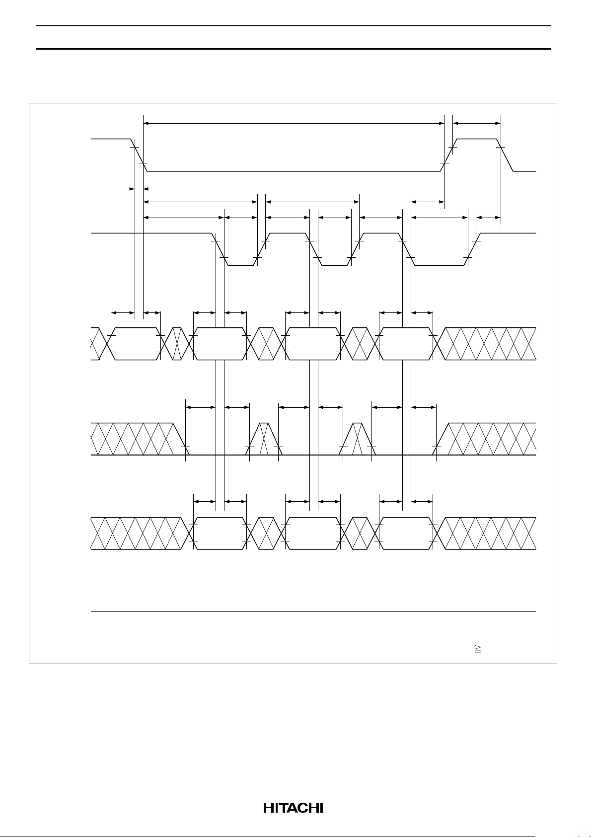
Self Refresh Cycle (L-version)*
23, 24, 25, 26
RAS
Dout
t
RP
t
RASS
t
RPS
t
RPC
t
T
t
CP
t
CSR
t
CHS
t
CRP
t
OFF
t
OFR
High-Z
UCAS
LCAS
t
WRP
t
WRH
WE

HM5164165 Series, HM5165165 Series
34
Package Dimensions
HM5164165J/LJ Series
HM5165165J/LJ Series (CP-50DA)
TBD
HM5164165TT/LTT Series
HM5165165TT/LTT Series (TTP-50DB)
0.13
M
0.10
0.80
50 26
125
20.95
21.35 Max
0.30 ± 0.10
1.20 Max
10.16
0.13 ± 0.05
11.76 ± 0.20
0° – 5°
1.15 Max
0.145 ± 0.05
Hitachi Code
JEDEC
EIAJ
Weight
(reference value)
TTP-50DB
—
—
0.51 g
0.28 ± 0.08
0.125 ± 0.04
Unit: mm
0.50 ± 0.10
0.68
0.80
Dimension including the plating thickness
Base material dimension

HM5164165 Series, HM5165165 Series
35
When using this document, keep the following in mind:
1. This document may, wholly or partially, be subject to change without notice.
2. All rights are reserved: No one is permitted to reproduce or duplicate, in any form, the whole or part of
this document without Hitachi’s permission.
3. Hitachi will not be held responsible for any damage to the user that may result from accidents or any other
reasons during operation of the user’s unit according to this document.
4. Circuitry and other examples described herein are meant merely to indicate the characteristics and
performance of Hitachi’s semiconductor products. Hitachi assumes no responsibility for any intellectual
property claims or other problems that may result from applications based on the examples described
herein.
5. No license is granted by implication or otherwise under any patents or other rights of any third party or
Hitachi, Ltd.
6. MEDICAL APPLICATIONS: Hitachi’s products are not authorized for use in MEDICAL
APPLICATIONS without the written consent of the appropriate officer of Hitachi’s sales company. Such
use includes, but is not limited to, use in life support systems. Buyers of Hitachi’s products are requested
to notify the relevant Hitachi sales offices when planning to use the products in MEDICAL
APPLICATIONS.
Hitachi, Ltd.
Semiconductor & IC Div.
Nippon Bldg., 2-6-2, Ohte-machi, Chiyoda-ku, Tokyo 100, Japan
Tel: Tokyo (03) 3270-2111
Fax: (03) 3270-5109
For further information write to:
Hitachi America, Ltd.
Semiconductor & IC Div.
2000 Sierra Point Parkway
Brisbane, CA. 94005-1835
U S A
Tel: 415-589-8300
Fax: 415-583-4207
Hitachi Europe GmbH
Continental Europe
Dornacher Straße 3
D-85622 Feldkirchen
München
Tel: 089-9 91 80-0
Fax: 089-9 29 30-00
Hitachi Europe Ltd.
Electronic Components Div.
Northern Europe Headquarters
Whitebrook Park
Lower Cookham Road
Maidenhead
Berkshire SL6 8YA
United Kingdom
Tel: 01628-585000
Fax: 01628-585160
Hitachi Asia Pte. Ltd.
16 Collyer Quay #20-00
Hitachi Tower
Singapore 049318
Tel: 535-2100
Fax: 535-1533
Hitachi Asia (Hong Kong) Ltd.
Unit 706, North Tower,
World Finance Centre,
Harbour City, Canton Road
Tsim Sha Tsui, Kowloon
Hong Kong
Tel: 27359218
Fax: 27306071
Cop
yrig
ht © Hitachi, Ltd., 1997. All rights reserved. Printed in Japan.

HM5164165 Series, HM5165165 Series
36
Revision Record
Rev. Date Contents of Modification Drawn by Approved by
0.0 Jul. 23, 1997 Initial issue J. Miyake M. Saeki
0.1 Oct. 24, 1997 AC Characteristics
Change order of notes
Change note numbers of tables
Correct errors
EDO page mode read cycke
 Loading...