Preliminary: The Specifications of this device are subject to change without notice. Please contact to your
nearest Hitachi’s sales Dept. regarding specifications
HM5164165 Series
HM5165165 Series
64M EDO DRAM (4-Mword × 16-bit)
8k refresh/4k refresh
ADE-203-802A(Z)
Preliminary
Rev. 0.1
Oct. 24, 1997
Description
The Hitachi HM5164165 Series, HM5165165 Series are 64M-bit dynamic RAMs organized as 4,194,304word × 16-bit. They have realized high performance and low power by employing CMOS process technology.
HM5164165 Series, HM5165165 Series offer Extended Data Out (EDO) Page Mode as a high speed access
mode. They have the package variations of standard 50-pin plastic SOJ and standerd 50-pin plastic TSOPII
Features
• Single 3.3 V supply: 3.3 V ± 0.3 V
• Access time: 50 ns/60 ns (max)
• Power dissipation
Active: 432 mW/396 mW (max) (HM5164165 Series)
: 504 mW/432 mW (max) (HM5165165 Series)
Standby : 1.8 mW (max) (CMOS interface)
: 0.54 mW (max) (L-version)
• EDO page mode capability
• Refresh cycles
RAS-only refresh
8192 cycles/64 ms (HM5164165)
/128 ms (HM5164165L) (L-version)
4096 cycles/64 ms (HM5165165)
/128 ms (HM5165165L) (L-version)
CBR/Hidden refresh
4096 cycles/64 ms (HM5164165, HM5165165)
/128 ms (HM5164165L, HM5165165L) (L-version)

HM5164165 Series, HM5165165 Series
2
• 4 variations of refresh
RAS-only refresh
CAS-before-RAS refresh
Hidden refresh
Self refresh (L-version)
• 2CAS-byte control
• Battery backup operation (L-version)
Ordering Information
Type No. Access time Package
HM5164165J-5*
HM5164165J-6*
50 ns
60 ns
400-mil 50-pin plastic SOJ (CP-50DA)
HM5164165LJ-5*
HM5164165LJ-6*
50 ns
60 ns
HM5165165J-5*
HM5165165J-6*
50 ns
60 ns
HM5165165LJ-5*
HM5165165LJ-6*
50 ns
60 ns
HM5164165TT-5
HM5164165TT-6
50 ns
60 ns
400-mil 50-pin plastic TSOP II (TTP-50DB)
HM5164165LTT-5
HM5164165LTT-6
50 ns
60 ns
HM5165165TT-5
HM5165165TT-6
50 ns
60 ns
HM5165165LTT-5
HM5165165LTT-6
50 ns
60 ns
Note: Under development.

HM5164165 Series, HM5165165 Series
3
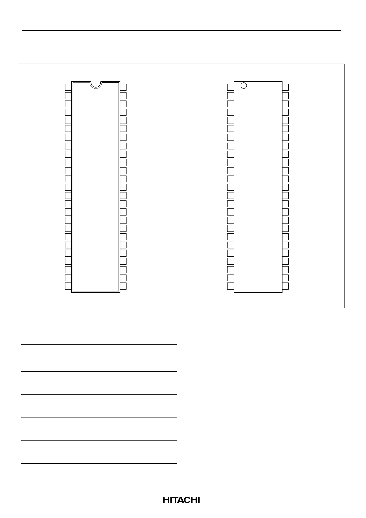
Pin Arrangement (HM5164165 Series)
V
SS
I/O15
I/O14
I/O13
I/O12
V
SS
I/O11
I/O10
I/O9
I/O8
NC
V
SS
LCAS
UCAS
OE
NC
NC
A12
A11
A10
A9
A8
A7
A6
V
SS
1
2
3
4
5
6
7
8
9
10
11
12
13
14
15
16
17
18
19
20
21
22
23
24
25
50
49
48
47
46
45
44
43
42
41
40
39
38
37
36
35
34
33
32
31
30
29
28
27
26
V
CC
I/O0
I/O1
I/O2
I/O3
V
CC
I/O4
I/O5
I/O6
I/O7
NC
V
CC
WE
RAS
NC
NC
NC
NC
A0
A1
A2
A3
A4
A5
V
CC
50-pin TSOP
(Top view)
V
SS
I/O15
I/O14
I/O13
I/O12
V
SS
I/O11
I/O10
I/O9
I/O8
NC
V
SS
LCAS
UCAS
OE
NC
NC
A12
A11
A10
A9
A8
A7
A6
V
SS
VCC
I/O0
I/O1
I/O2
I/O3
V
CC
I/O4
I/O5
I/O6
I/O7
NC
V
CC
WE
RAS
NC
NC
NC
NC
A0
A1
A2
A3
A4
A5
V
CC
50-pin SOJ
(Top view)
50
49
48
47
46
45
44
43
42
41
40
39
38
37
36
35
34
33
32
31
30
29
28
27
26
1
2
3
4
5
6
7
8
9
10
11
12
13
14
15
16
17
18
19
20
21
22
23
24
25
Pin Description
Pin name Function
A0 to A12 Address input
— Row/Refresh address A0 to A12
— Column address A0 to A8
I/O0 to I/O15 Data input/output
RAS Row address strobe
UCAS, LCAS Column address strobe
WE Write enable
OE Output enable
V
CC
Power supply
V
SS
Ground
NC No connection

HM5164165 Series, HM5165165 Series
4
Pin Arrangement (HM5165165 Series)
V
SS
I/O15
I/O14
I/O13
I/O12
V
SS
I/O11
I/O10
I/O9
I/O8
NC
V
SS
LCAS
UCAS
OE
NC
NC
NC
A11
A10
A9
A8
A7
A6
V
SS
1
2
3
4
5
6
7
8
9
10
11
12
13
14
15
16
17
18
19
20
21
22
23
24
25
50
49
48
47
46
45
44
43
42
41
40
39
38
37
36
35
34
33
32
31
30
29
28
27
26
V
CC
I/O0
I/O1
I/O2
I/O3
V
CC
I/O4
I/O5
I/O6
I/O7
NC
V
CC
WE
RAS
NC
NC
NC
NC
A0
A1
A2
A3
A4
A5
V
CC
50-pin TSOP
(Top view)
V
SS
I/O15
I/O14
I/O13
I/O12
V
SS
I/O11
I/O10
I/O9
I/O8
NC
V
SS
LCAS
UCAS
OE
NC
NC
NC
A11
A10
A9
A8
A7
A6
V
SS
VCC
I/O0
I/O1
I/O2
I/O3
V
CC
I/O4
I/O5
I/O6
I/O7
NC
V
CC
WE
RAS
NC
NC
NC
NC
A0
A1
A2
A3
A4
A5
V
CC
50-pin SOJ
(Top view)
50
49
48
47
46
45
44
43
42
41
40
39
38
37
36
35
34
33
32
31
30
29
28
27
26
1
2
3
4
5
6
7
8
9
10
11
12
13
14
15
16
17
18
19
20
21
22
23
24
25
Pin Description
Pin name Function
A0 to A11 Address input
— Row/Refresh address A0 to A11
— Column address A0 to A9
I/O0 to I/O15 Data input/output
RAS Row address strobe
UCAS, LCAS Column address strobe
WE Write enable
OE Output enable
V
CC
Power supply
V
SS
Ground
NC No connection

HM5164165 Series, HM5165165 Series
5
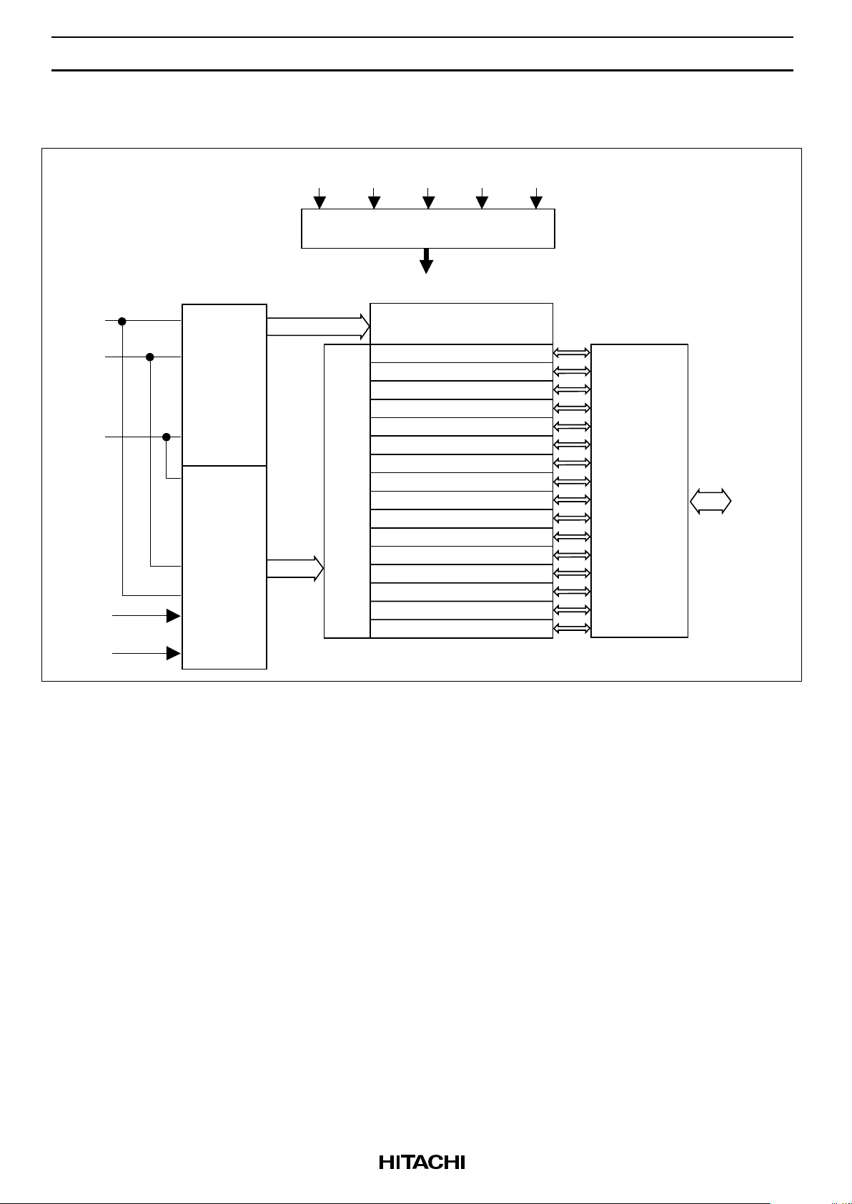
Block Diagram (HM5164165 Series)
•
•
•
•
•
•
A0
A1
to
A8
A9
to
A12
Timing and control
RAS UCAS LCAS WE OE
Column
address
buffers
Row
address
buffers
I/O buffers
I/O0
to
I/O15
Column decoder
Row decoder
4M array
4M array
4M array
4M array
4M array
4M array
4M array
4M array
4M array
4M array
4M array
4M array
4M array
4M array
4M array
4M array

HM5164165 Series, HM5165165 Series
6
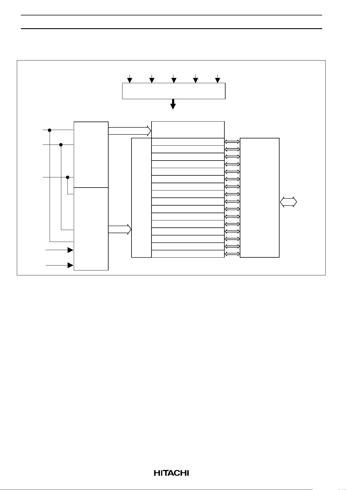
Block Diagram (HM5165165 Series)
•
•
•
•
•
•
A0
A1
to
A9
Timing and control
RAS UCAS LCAS WE OE
Column
address
buffers
Row
address
buffers
I/O buffers
I/O0
to
I/O15
Column decoder
Row decoder
4M array
4M array
4M array
4M array
4M array
4M array
4M array
4M array
4M array
4M array
4M array
4M array
4M array
4M array
4M array
4M array
A10
A11

HM5164165 Series, HM5165165 Series
7
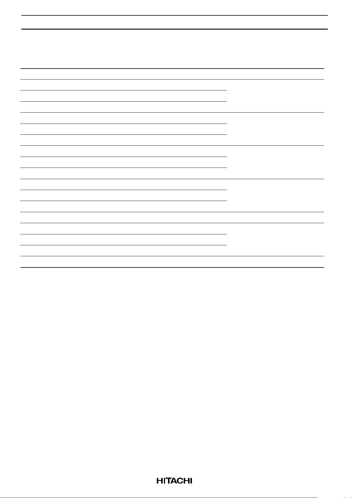
Operation Table
RAS LCAS UCAS WE OE I/O 0 to I/O 7 I/O 8 to I/O 15 Operation
H ××××High-Z High-Z Standby
L L H H L Dout High-Z Read cycle
L H L H L High-Z Dout
LLLHLDout Dout
LLHL*
2
×Din × Early write cycle
LHLL*
2
×× Din
LLLL*
2
×Din Din
LLHL*
2
H Din × Delayed write cycle
LHLL*
2
H× Din
LLLL*
2
H Din Din
L L H H to L L to H Dout/Din High-Z Read-modify-write cycle
L H L H to L L to H High-Z Dout/Din
LLLH to LL to HDout/Din Dout/Din
LHH××High-Z High-Z RAS-only refresh cycle
H to L H L H × High-Z High-Z CAS-before-RAS refresh cycle or
H to L L H H × High-Z High-Z Self refresh cycle (L-version)
H to L L L H × High-Z High-Z
L L L H H High-Z High-Z Read cycle (Output disabled)
Notes: 1. H: VIH (inactive) L: VIL (active) ×: VIH or V
IL
2. t
WCS
≥ 0 ns: Early write cycle
t
WCS
< 0 ns: Delayed write cycle
3. Mode is determined by the OR function of the UCAS and LCAS. (Mode is set by the earliest of
UCAS and LCAS active edge and reset by the latest of UCAS and LCAS inactive edge.) However
write operation and output High-Z control are done independently by each UCAS, LCAS.
ex. if RAS = H to L, LCAS = L, UCAS = H, then CAS-before-RAS refresh cycle is selected.

HM5164165 Series, HM5165165 Series
8
Absolute Maximum Ratings
Parameter Symbol Value Unit
Terminal voltage on any pin relative to V
SS
V
T
–0.5 to VCC + 0.5 ( 4.6 V (max)) V
Power supply voltage relative to V
SS
V
CC
–0.5 to +4.6 V
Short circuit output current Iout 50 mA
Power dissipation P
T
1.0 W
Storage temperature Tstg –55 to +125 °C
DC Operating Conditions
Parameter Symbol Min Typ Max Unit Notes
Supply voltage V
CC
3.0 3.3 3.6 V 1, 2
V
SS
000 V2
Input high voltage V
IH
2.0 — VCC + 0.3 V 1
Input low voltage V
IL
–0.3 — 0.8 V 1
Ambient temperature range Ta 0 — 70 ˚C
Notes: 1. All voltage referred to VSS.
2. The supply voltage with all V
CC
pins must be on the same level. The supply voltage with all VSS pins
must be on the same level.

HM5164165 Series, HM5165165 Series
9
DC Characteristics (HM5164165 Series)
HM5164165
-5 -6
Parameter Symbol Min Max Min Max Unit Test conditions
Operating current*
1, *2
I
CC1
— 120 — 110 mA tRC = min
Standby current I
CC2
— 2 — 2 mA TTL interface
RAS, UCAS, LCAS = V
IH
Dout = High-Z
— 0.5 — 0.5 mA CMOS interface
RAS, UCAS,
LCAS V
CC
– 0.2 V
Dout = High-Z
Standby current
(L-version)
I
CC2
— 150 — 150 µA CMOS interface
RAS, UCAS,
LCAS V
CC
– 0.2 V
Dout = High-Z
RAS-only refresh current*
2
I
CC3
— 120 — 110 mA tRC = min
Standby current*
1
I
CC5
—5 —5 mARAS = V
IH
UCAS, LCAS = V
IL
Dout = enable
CAS-before-RAS refresh
current
I
CC6
— 120 — 110 mA tRC = min
EDO page mode current*
1, *3
I
CC7
— 120 — 110 mA RAS = VIL , CAS cycle,
t
HPC
= t
HPC
min
Battery backup current*
4
(Standby with CBR refresh)
(L-version)
I
CC10
— 500 — 500 µA CMOS interface
Dout = High-Z
CBR refresh: t
RC
= 31.3 µs
t
RAS
0.3 µs
Self refresh mode current
(L-version)
I
CC11
— 400 — 400 µA CMOS interface
RAS, UCAS, LCAS 0.2 V
Dout = High-Z
Input leakage current I
LI
–5 5 –5 5 µA 0 V Vin VCC + 0.3 V
Output leakage current I
LO
–5 5 –5 5 µA 0 V Vout V
CC
Dout = disable
Output high voltage V
OH
2.4 V
CC
2.4 V
CC
V High Iout = –2 mA
Output low voltage V
OL
0 0.4 0 0.4 V Low Iout = 2 mA
Notes: 1. ICC depends on output load condition when the device is selected. ICC max is specified at the output
open condition.
2. Address can be changed once or less while RAS = V
IL
.
3. Measured with one sequential address change per EDO cycle, t
HPC
.
4. V
IH
VCC – 0.2 V, 0 V VIL 0.2 V.

HM5164165 Series, HM5165165 Series
10
DC Characteristics (HM5165165 Series)
HM5165165
-5 -6
Parameter Symbol Min Max Min Max Unit Test conditions
Operating current*
1, *2
I
CC1
— 140 — 120 mA tRC = min
Standby current I
CC2
— 2 — 2 mA TTL interface
RAS, UCAS, LCAS = V
IH
Dout = High-Z
— 0.5 — 0.5 mA CMOS interface
RAS, UCAS,
LCAS V
CC
– 0.2 V
Dout = High-Z
Standby current
(L-version)
I
CC2
— 150 — 150 µA CMOS interface
RAS, UCAS,
LCAS V
CC
– 0.2 V
Dout = High-Z
RAS-only refresh current*
2
I
CC3
— 140 — 120 mA tRC = min
Standby current*
1
I
CC5
—5 —5 mARAS = V
IH
UCAS, LCAS = V
IL
Dout = enable
CAS-before-RAS refresh
current
I
CC6
— 140 — 120 mA tRC = min
EDO page mode current*
1, *3
I
CC7
— 120 — 110 mA RAS = VIL , CAS cycle,
t
HPC
= t
HPC
min
Battery backup current*
4
(Standby with CBR refresh)
(L-version)
I
CC10
— 500 — 500 µA CMOS interface
Dout = High-Z
CBR refresh: t
RC
= 31.3 µs
t
RAS
0.3 µs
Self refresh mode current
(L-version)
I
CC11
— 400 — 400 µA CMOS interface
RAS, UCAS, LCAS 0.2 V
Dout = High-Z
Input leakage current I
LI
–5 5 –5 5 µA 0 V Vin VCC + 0.3 V
Output leakage current I
LO
–5 5 –5 5 µA 0 V Vout V
CC
Dout = disable
Output high voltage V
OH
2.4 V
CC
2.4 V
CC
V High Iout = –2 mA
Output low voltage V
OL
0 0.4 0 0.4 V Low Iout = 2 mA
Notes: 1. ICC depends on output load condition when the device is selected. ICC max is specified at the output
open condition.
2. Address can be changed once or less while RAS = V
IL
.
3. Measured with one sequential address change per EDO cycle, t
HPC
.
4. V
IH
VCC – 0.2 V, 0 V VIL 0.2 V.

HM5164165 Series, HM5165165 Series
11
Capacitance (Ta = 25°C, VCC = 3.3 V ± 0.3 V)
Parameter Symbol Min Typ Max Unit Notes
Input capacitance (Address) C
I1
——5 pF1
Input capacitance (Clocks) C
I2
——7 pF1
Output capacitance (Data-in, Data-out) C
I/O
— — 7 pF 1, 2
Notes : 1. Capacitance measured with Boonton Meter or effective capacitance measuring method.
2. RAS, UCAS and LCAS = V
IH
to disable Dout.
 Loading...