

HIT HD74LVCR2245A Datasheet

HD74LVCR2245A
Octal Bidirectional Transceivers with 3–state Outputs
ADE-205-235A (Z)
Preliminary
2nd. Edition
January 1999
Description
The HD74LVCR2245A has eight buffers with three state outputs in a 20 pin package. When (T / R) is
high, data flows from the A inputs to the B outputs, and when (T / R) is low, data flows from the B inputs
to the A outputs. A and B bus are separated by making enable input (OE) high level.
All outputs, which are designed to sink up to 12 mA, include equivalent 26 Ω resistors to reduce overshoot
and undreshoot.
When VCC is between 0 and 1.5 V, the device is in the high impedance state during power up or power
down.
Low voltage and high speed operation is suitable at battery drive product (note type personal computer) and
low power consumption extends the life of a battery for long time operation.
Features
• VCC = 1.65 to 5.5 V
• All inputs VIH (Max) = 5.5 V (@VCC = 0 to 5.5 V)
• All inputs / outputs V
• Typical VOL ground bounce < 0.8 V (@VCC = 3.3 V, Ta = 25°C)
• Typical VOH undershoot > 2.0 V (@VCC = 3.3 V, Ta = 25°C)
• High output current ±12 mA (@VCC = 3.0 to 5.5 V)
• All outputs have equivalent 26 Ω series resistors, so no external resistors are required
(Max) = 5.5 V (@VCC = 0 V or output off state)
I / O
HD74LVCR2245A
Function Table
Inputs Operation
OE T / R
L L B data to A bus
L H A data to B bus
HX Z
H : High level
L : Low level
X : Immaterial
Z : High impedance
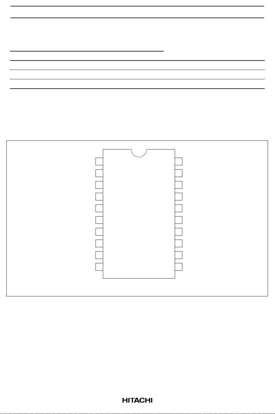
Pin Arrangement
V
T / R
1
20
CC
A0
A1
A2
A3
A4
A5
A6
A7
GND
10
2
3
4
5
6
7
8
9
(Top view)
19
18
17
16
15
14
13
12
11
OE
B0
B1
B2
B3
B4
B5
B6
B7
2
HD74LVCR2245A
Absolute Maximum Ratings
Item Symbol Ratings Unit Conditions
Supply voltage V
Input voltage V
Output voltage V
Input diode current I
Output diode current I
Output current I
VCC, GND current ICC or I
CC
I
O
IK
OK
O
GND
Storage temperature Tstg –65 to 150 °C
Note: The absolute maximum ratings are values which must not individually be exceeded, and furthermore
no two of which may be realized at the same time.
Recommended Operating Conditions
–0.5 to 7.0 V
–0.5 to 7.0 V
–0.5 to 7.0 V Output “Z” or VCC : OFF
–0.5 to VCC+0.5 Output “H” or “L”
–50 mA VI < 0
–50 mA VO < 0
±50 mA
±100 mA
Item Symbol Ratings Unit Conditions
Supply voltage V
CC
1.65 to 5.5 V At operation
1.5 to 5.5 Data retention only
Input voltage V
Output voltage V
Output current I
I
O
OH
0 to 5.5 V
0 to 5.5 V Output “Z” or VCC : OFF
0 to V
CC
Output “H” or “L”
–2 mA VCC = 1.65 V
–4 VCC = 2.3 V
–8 VCC = 2.7 V
–12 VCC = 3.0 to 5.5 V
I
OL
2V
4V
8V
= 1.65 V
CC
= 2.3 V
CC
= 2.7 V
CC
12 VCC = 3.0 to 5.5 V
Input rise / fall time tr, t
f
0 to 6 ns / V
Operating temperature Ta –40 to +85 °C
3
HD74LVCR2245A
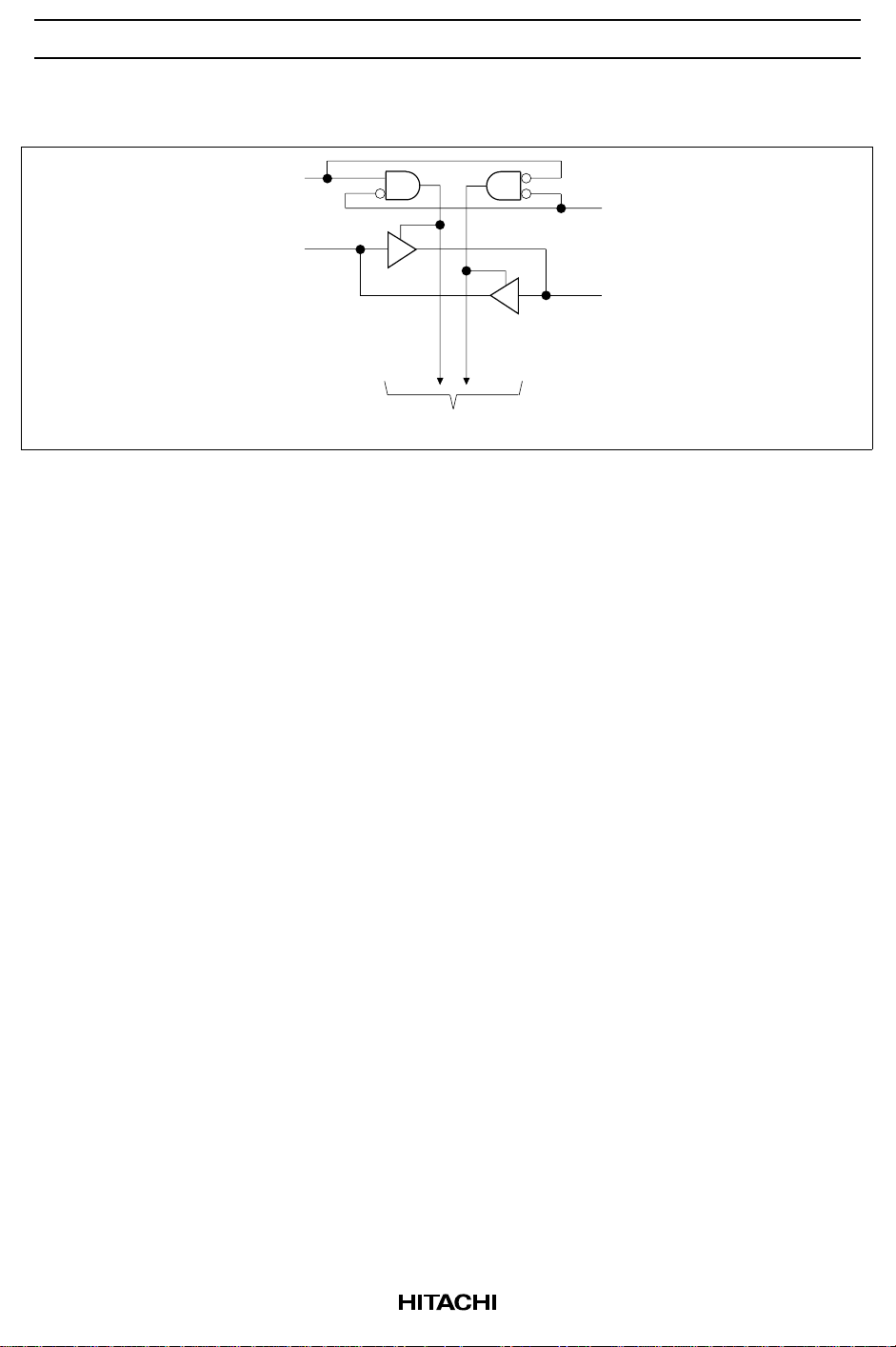
E
Logic Diagram
T / R
A0
1
19
O
2
18
B0
To seven other channels
4
 Loading...