

HIT HD74LVC533 Datasheet
HD74LVC533
Octal D-type Transparent Latches with 3-state Outputs
ADE-205-070B(Z)
Rev.2
September 1995
Description
The HD74LVC533 has eight D type latches with three state outputs in a 20 pin package. When the latch
enable input is high, the Q outputs will follow the D inputs. When the latch enable goes low, data at the D
inputs will be retained at the outputs until latch enable returns high again. When a high logic level is
applied to the output control input, all outputs go to a high impedance state, regardless of what signals are
present at the other inputs and the state of the storage elements. Low voltage and high speed operation is
suitable at the battery drive product (note type personal computer) and low power consumption extends the
life of a battery for long time operation.
Features
• VCC = 2.0 V to 5.5 V
• All inputs VIH (Max.) = 5.5 V (@VCC = 0 V to 5.5 V)
• Typical VOL ground bounce < 0.8 V (@VCC = 3.3 V, Ta = 25°C)
• Typical VOH undershoot > 2.0 V (@VCC = 3.3 V, Ta = 25°C)
• High output current ±24 mA (@VCC = 3.0 V to 5.5 V)
Function Table
Inputs
G LE D Output Q
HXXZ
LHLH
LHHL
LLXQ
H : High level
L : Low level
X : Immaterial
Z : High impedance
Q
: Level of Q before the indicated steady input conditions were established.
0
0
HD74LVC533
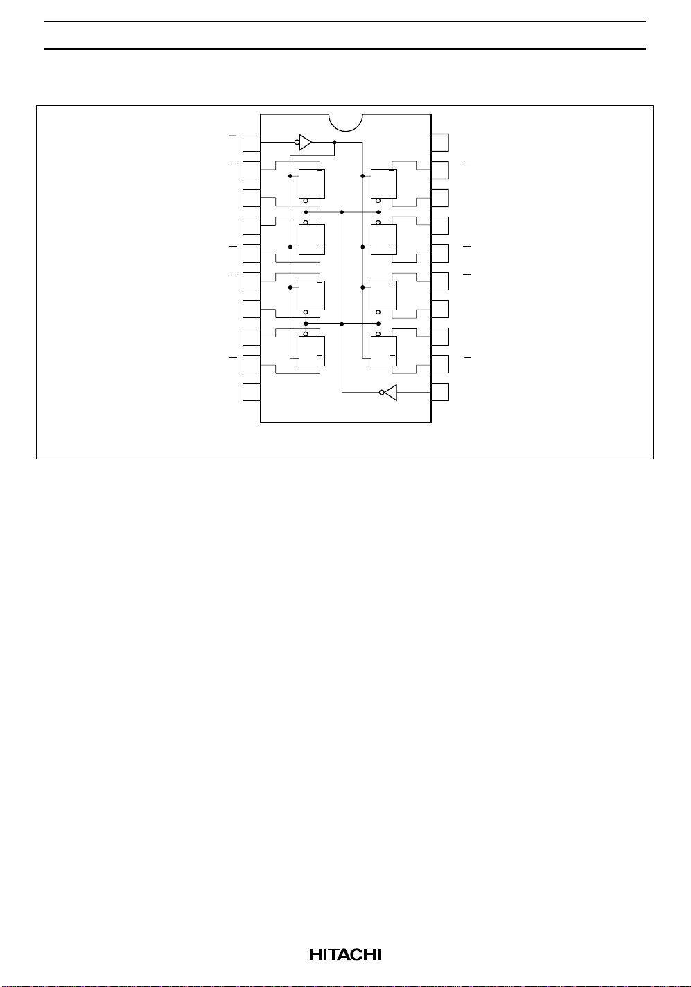
Pin Arrangement
V
1
G
20
CC
1Q
1D
2D
2Q
3Q
3D
4D
4Q
GND
10
2
3
4
5
6
7
8
9
Q Q
G
D
D
G
Q Q
Q
G
D
D
G
Q Q
G
D
D
G
G
Q
D
D
G
19
18
17
16
15
14
13
12
11
8Q
8D
7D
7Q
6Q
6D
5D
5Q
LE
(Top view)
2
HD74LVC533
Absolute Maximum Ratings
Item Symbol Ratings Unit Conditions
Supply voltage V
Input diode current I
Input voltage V
Output diode current I
Output voltage V
Output current I
VCC, GND current / pin ICC or I
CC
IK
I
OK
O
O
GND
Storage temperature Tstg –65 to +150 °C
Note: The absolute maximum ratings are values which must not individually be exceeded, and furthermore,
no two of which may be realized at the same time.
Recommended Operating Conditions
–0.5 to 6.0 V
–50 mA VI = –0.5 V
–0.5 to 6.0 V
–50 mA VO = –0.5 V
50 mA VO = VCC+0.5 V
–0.5 to VCC +0.5 V
±50 mA
100 mA
Item Symbol Ratings Unit Conditions
Supply voltage V
CC
1.5 to 5.5 V Data retention
2.0 to 5.5 V At operation
Input / output voltage V
I
V
O
0 to 5.5 V G, LE, D
0 to V
CC
V Q
Operating temperature Ta –40 to 85 °C
Output current I
Input rise / fall time
*1
OH
I
OL
tr, t
f
–12 mA VCC = 2.7 V
*2
–24
mA VCC = 3.0 V to 5.5 V
12 mA VCC = 2.7 V
*2
24
mA VCC = 3.0 V to 5.5 V
10 ns/V
Notes: 1. This item guarantees maximum limit when one input switches.
Waveform : Refer to test circuit of switching characteristics.
2. duty cycle ≤ 50%
3
 Loading...