

HIT HD74LVC244A Datasheet
HD74LVC244A
Octal Buffers / Line Drivers with 3-state Outputs
ADE-205-110B(Z)
3rd Edition
December 1996
Description
The HD74LVC244A has eight line drivers with three state outputs in a 20 pin package. This device is a
non inverting buffer and has two active low enables (1G and 2G). Each enable independently controls four
buffers. Low voltage and high speed operation is suitable at the battery drive product (note type personal
computer) and low power consumption extends the life of a battery for long time operation.
Features
• VCC = 2.0 V to 5.5 V
• All inputs VIH (Max.) = 5.5 V (@VCC = 0 V to 5.5 V)
• All outputs V
• Typical VOL ground bounce < 0.8 V (@VCC = 3.3 V, Ta = 25°C)
• Typical VOH undershoot > 2.0 V (@VCC = 3.3 V, Ta = 25°C)
• High output current ±24 mA (@VCC = 3.0 V to 5.5 V)
(Max.) = 5.5 V (@VCC = 0 V or output off state)
OUT
Function Table
Inputs
G A Output Y
HX Z
LHH
LL L
H : High level
L : Low level
X : Immaterial
Z : High impedance
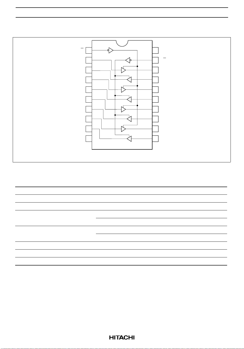
HD74LVC244A
Pin Arrangement
1G
1A1
2Y4
1A2
2Y3
1A3
2Y2
V
1
2
3
4
5
6
7
20
19
18
17
16
15
14
CC
2G
1Y1
2A4
1Y2
2A3
1Y3
1A4
2Y1
GND
8
9
10
13
12
11
2A2
1Y4
2A1
(Top view)
Absolute Maximum Ratings
Item Symbol Ratings Unit Conditions
Supply voltage V
Input diode current I
Input voltage V
Output diode current I
Output voltage V
Output current I
VCC, GND current / pin I
IK
OK
O
CC
CC
I
O
or I
GND
Storage temperature Tstg –65 to 150 °C
Note: The absolute maximum ratings are values which must not individually be exceeded, and furthermore,
no two of which may be realized at the same time.
–0.5 to 6.0 V
–50 mA VI = –0.5 V
–0.5 to 6.0 V
–50 mA VO = –0.5 V
50 mA VO = V
+0.5 V
CC
–0.5 to VCC +0.5 V Output "H" or "L"
–0.5 to 6.0 V Output "Z" VCC:OFF
±50 mA
100 mA
2
HD74LVC244A
Recommended Operating Conditions
Item Symbol Ratings Unit Conditions
Supply voltage V
Input / output voltage V
CC
I
V
O
Operating temperature Ta –40 to 85 °C
Output current I
Input rise / fall time
*1
OH
I
OL
tr, t
f
Notes: 1. This item guarantees maximum limit when one input switches.
Waveform : Refer to test circuit of switching characteristics.
2. duty cycle ≤ 50%
1.5 to 5.5 V Data retention
2.0 to 5.5 V At operation
0 to 5.5 V G, A
0 to V
CC
V Output "H" or "L"
0 to 5.5 V Output "Z" or VCC:OFF
–12 mA VCC = 2.7 V
*2
–24
mA VCC = 3.0 V to 5.5 V
12 mA VCC = 2.7 V
*2
24
mA VCC = 3.0 V to 5.5 V
10 ns/V
3
 Loading...