

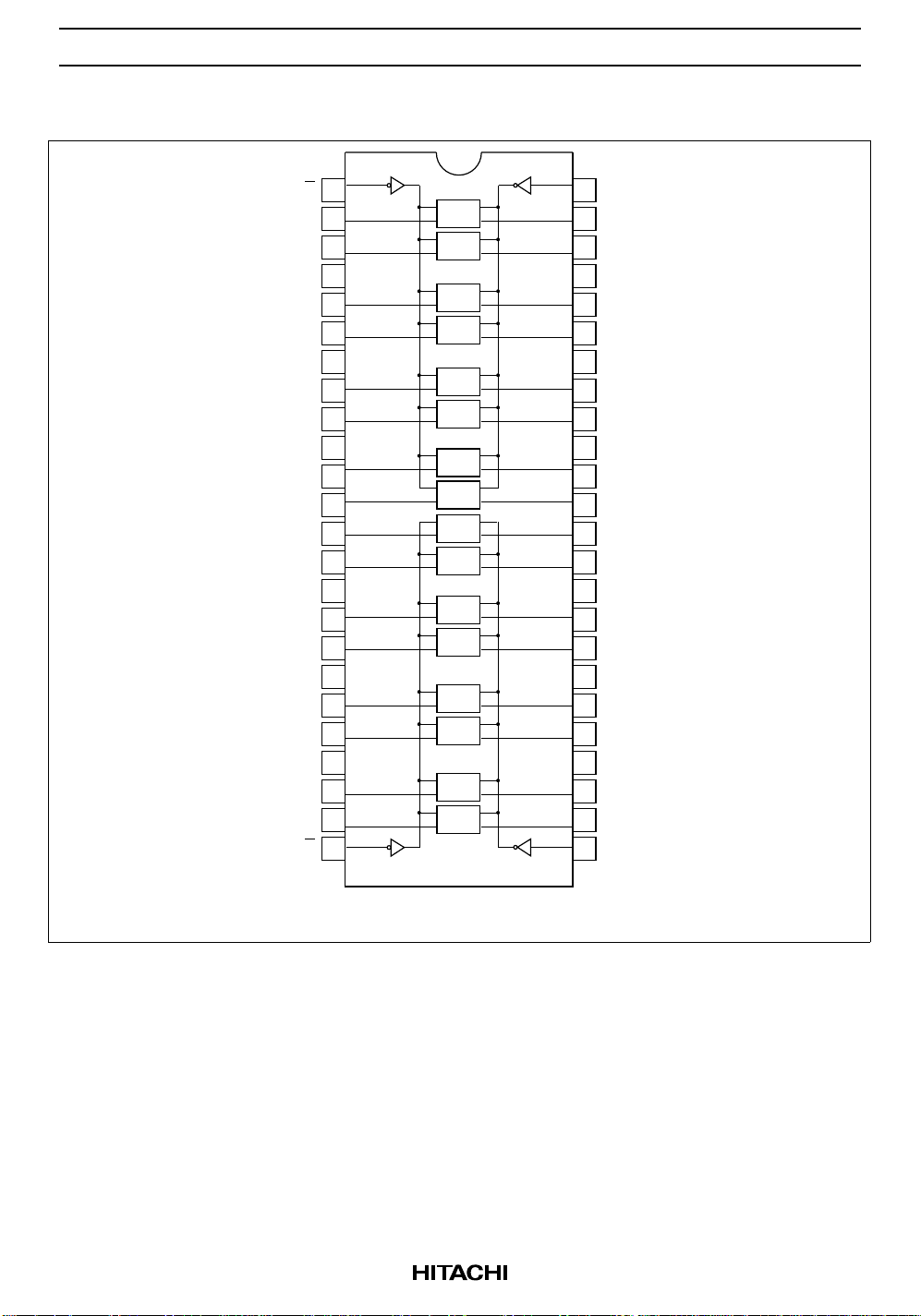
HD74LVC16373A
16-bit D-type Transparent Latches with 3-state Outputs
ADE-205-121B(Z)
3rd Edition
December 1996
Description
The HD74LVC16373A has sixteen D type latches with three state outputs in a 48 pin package. When the
latch enable input is high, the Q outputs will follow the D inputs. When the latch enable goes low, data at
the D inputs will be retained at the outputs until latch enable returns high again. When a high logic level is
applied to the output control input (1G, 2G), all outputs go to a high impedance state, regardless of what
signals are present at the other inputs and the state of the storage elements. Low voltage and high speed
operation is suitable at the battery drive product (note type personal computer) and low power consumption
extends the life of a battery for long time operation.
Features
• VCC = 2.0 V to 5.5 V
• All inputs VIH (Max.) = 5.5 V (@VCC = 0 V to 5.5 V)
• All outputs V
• Typical VOL ground bounce < 0.8 V (@VCC = 3.3 V, Ta = 25°C)
• Typical VOH undershoot > 2.0 V (@VCC = 3.3 V, Ta = 25°C)
• High output current ±24 mA (@VCC = 3.0 V to 5.5 V)
(Max.) = 5.5 V (@VCC = 0 V or output off state)
OUT
Function Table
Inputs
G LE D Output Q
HXXZ
LHLL
LHHH
LLXQ
H: High level
L: Low level
X: Immaterial
Z: High impedance
Q
: Level of Q before the indicated steady input conditions were established.
0
0
HD74LVC16373A
Pin Arrangement
1G
1Q1
1Q2
GND
1Q3
1Q4
V
CC
1Q5
1Q6
GND
1Q7
1Q8
2Q1
2Q2
GND
2Q3
2Q4
V
CC
2Q5
2Q6
GND
2Q7
2Q8
2G
10
11
12
13
14
15
16
17
18
19
20
21
22
23
24
1LE
1
2
3
4
5
6
7
8
9
G
Q
D
G
Q
D
G
Q
D
G
Q
D
G
Q
D
G
Q
D
G
Q
D
G
Q
D
G
Q
D
G
Q
D
G
Q
D
G
Q
D
G
Q
D
G
Q
D
G
Q
D
G
Q
D
48
47
46
45
44
43
42
41
40
39
38
37
36
35
34
33
32
31
30
29
28
27
26
25
1D1
1D2
GND
1D3
1D4
V
CC
1D5
1D6
GND
1D7
1D8
2D1
2D2
GND
2D3
2D4
V
CC
2D5
2D6
GND
2D7
2D8
2LE
(Top view)
2
HD74LVC16373A
Absolute Maximum Ratings
Item Symbol Ratings Unit Conditions
Supply voltage V
Input diode current I
Input voltage V
Output diode current I
Output voltage V
Output current I
VCC, GND current / pin ICC or I
CC
IK
I
OK
O
O
GND
Storage temperature Tstg –65 to +150 °C
Note: The absolute maximum ratings are values which must not individually be exceeded, and furthermore,
no two of which may be realized at the same time.
Recommended Operating Conditons
–0.5 to 6.0 V
–50 mA VI = –0.5 V
–0.5 to 6.0 V
–50 mA VO = –0.5 V
50 mA VO = VCC+0.5 V
–0.5 to VCC +0.5 V Output "H" or "L"
–0.5 to 6.0 V Output "Z" or VCC:OFF
±50 mA
100 mA
Item Symbol Ratings Unit Conditions
Supply voltage V
CC
1.5 to 5.5 V Data hold
2.0 to 5.5 V At operation
Input / output voltage V
I
V
O
0 to 5.5 V G, LE, D
0 to V
CC
V Output "H" or "L"
0 to 5.5 V Output "Z" or VCC:OFF
Operating temperature Ta –40 to 85 °C
Output current I
Input rise / fall time
*1
OH
I
OL
tr, t
f
–12 mA VCC = 2.7 V
*2
–24
mA VCC = 3.0 V to 5.5 V
12 mA VCC = 2.7 V
*2
24
mA VCC = 3.0 V to 5.5 V
10 ns/V
Notes: 1. This item guarantees maximum limit when one input switches.
Waveform : Refer to test circuit of switching characteristics.
2. duty cycle ≤ 50%
3

HD74LVC16373A
Electrical Characteristics
Item Symbol V
Input voltage V
Output voltage V
Input current I
Off state output current I
Output leak current I
Quiescent supply current I
V
V
∆I
IH
IL
OH
OL
IN
OZ
OFF
CC
CC
Ta = –40 to 85°C
(V) Min Max Unit Test Conditions
CC
2.7 to 3.6 2.0 — V
4.5 to 5.5 VCC×0.7 — V
2.7 to 3.6 — 0.8 V
4.5 to 5.5 — VCC×0.3 V
2.7 to 5.5 VCC–0.2 — V IOH = –100 µA
2.7 2.2 — V IOH = –12 mA
3.0 2.4 — V
3.0 2.2 — V IOH = –24 mA
4.5 3.8 — V
2.7 to 5.5 — 0.2 V IOL = 100 µA
2.7 — 0.4 V IOL = 12 mA
3.0 — 0.55 V IOL = 24 mA
4.5 — 0.55 V
0 to 5.5 — ±5.0 µAVIN = 5.5 V or GND
2.7 to 5.5 — ±5.0 µAVIN = VCC, GND
V
= 5.5 V or GND
OUT
0—20µAVIN / V
2.7 to 3.6 — ±20 µAVIN / V
= 5.5 V
OUT
= 3.6 to 5.5 V
OUT
2.7 to 5.5 — 20 µAVIN = VCC or GND
3.0 to 3.6 — 500 µAVIN = one input at(VCC–0.6)V,
other inputs at V
or GND
CC
4

Switching Characteristics
Ta = –40 to 85°C
Item Symbol V
Propagation delay time t
Output enable time t
PLH
t
PHL
t
PLH
t
PHL
ZH
tZL3.3±0.3 1.5 — 7.0 ns
Output disable time t
HZ
tLZ3.3±0.3 1.5 — 7.0 ns
Setup time t
Hold time t
Pulse width t
Between output pins skew *1t
Input capacitance C
Output capacitance C
t
su
h
w
OSLH
OSHL
IN
O
Note: 1. This parameter is characterized but not tested.
tos
LH
= | t
PLHm
– t
|, tosHL = | t
PLHn
(V) Min Typ Max Unit From (Input) To (Output)
CC
2.7 — — 7.7 ns D Q
3.3±0.3 1.5 — 7.0 ns
5.0±0.5 — — 5.5 ns
2.7 — — 8.0 ns LE Q
3.3±0.3 2.0 — 7.0 ns
5.0±0.5 — — 5.5 ns
2.7 — — 8.0 ns GQ
5.0±0.5 — — 6.0 ns
2.7 — — 8.0 ns GQ
5.0±0.5 — — 6.0 ns
2.7 2.0 — — ns
3.3±0.3 2.0 — — ns
5.0±0.5 2.0 — — ns
2.7 1.5 — — ns
3.3±0.3 1.5 — — ns
5.0±0.5 1.5 — — ns
2.7 3.0 — — ns
3.3±0.3 3.0 — — ns
5.0±0.5 3.0 — — ns
2.7 — — — ns
3.3±0.3 — — 1.0 ns
5.0±0.5 — — 1.0 ns
2.7 — 3.0 — pF
2.7 — 15.0 — pF
– t
PHLn
|
PHLm
HD74LVC16373A
5
HD74LVC16373A
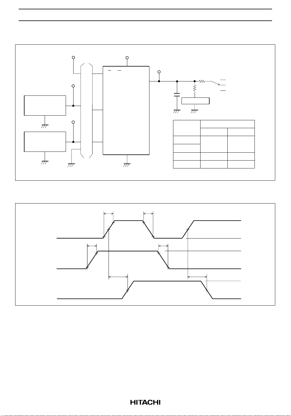
Test Circuit
V
CC
V
CC
1G, 2G
Input
1Q1 to 2Q8
Pulse Generator
Z = 50
out
Ω
1D1 to 2D8
Input
See Fuction Table
Pulse Generator
Z = 50
out
Ω
1LE, 2LE
Note: 1. CL includes probe and jig capacitance.
Waveforms – 1
t
r
90 %
90 %
V
90 %
ref
Input LE
Input D
10 %
t
r
t
f
90 %
Output
10 %
t
C =
L
50 pF
f
Ω
50 Scope
Symbol
t / t
PLH PHL
t / t / t
su h w
t / t
ZH HZ
t / t
ZL LZ
V
500
450
ref
Ω
S1
Ω
Vcc=2.7V,
3.3±0.3V
OPEN
GND
6 V
OPEN
*1
See under table
GND
S1
Vcc=5.0±0.5V
OPEN
GND
2×Vcc
V
GND
V
IH
IH
6
Output Q
10 %
t
PLH
10 %
t
PHL
V
ref
V
ref
GND
V
OH
V
OL

Waveforms – 2
Input LE
Input D
Output Q
Waveforms – 3
t
r
10 %
10 %
90 %
t
HD74LVC16373A
V
IH
r
V
t
90 %
ref
PLH
V
ref
90 %
t
f
V
ref
10 %
t
PHL
V
ref
GND
V
IH
GND
V
OH
V
OL
Input LE
10 %
Input D
Notes: 1. tr = 2.5 ns, tf = 2.5 ns
2. Input waveform : PRR = 10 MHz, duty cycle 50%
t
r
V
V
ref
90 % 90 %
ref
V
t
w
t
su
ref
t
f
V
IH
10 %
t
h
V
ref
GND
V
IH
GND
7

HD74LVC16373A
Waveforms – 4
t
f
Input G
90 %
V
ref
10 %
Waveform - A
Waveform - B
Notes: 1. tr = 2.5 ns, tf = 2.5 ns
2. Input waveform : PRR = 10 MHz, duty cycle 50%
3. Waveform – A shows input conditions such that the output is "L" level when enable by the
output control.
4. Waveform – B shows input conditions such that the output is "H" level when enable by the
output control.
t
r
V
GND
≈V
V
V
≈V
50%Vcc
Vcc
GND
IH
OH1
OL
OH
OL1
90 %
V
ref
10 %
t
ZL
V
ref
t
ZH
V
ref
t
t
HZ
LZ
TEST
V
IH
V
ref
V
OH1
V
OL1
V + 0.3 V
OL
V – 0.3 V
OH
Vcc=2.7V,
3.3±0.3V
2.7 V Vcc
1.5 V
3 V
GND
Vcc=5.0±0.5V
8
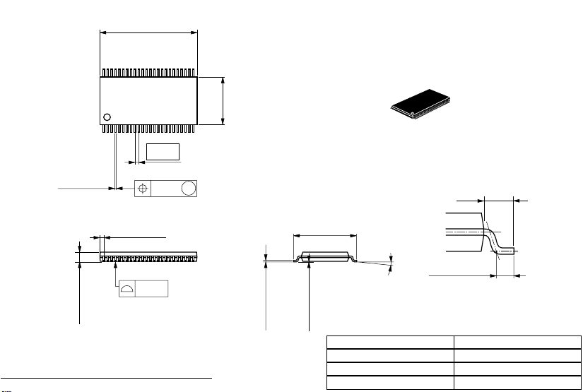
12.5
12.7 Max
Unit: mm
2548
6.10
*0.21
0.19
124
+0.04
–0.05
+0.03
–0.05
0.50
0.08
M
0.65 Max
0.10
1.20 Max
*Dimension including the plating thickness
Base material dimension
0.15 ± 0.04
*0.17 ± 0.05
8.10 ± 0.20
0.13 ± 0.05
Hitachi Code
JEDEC
EIAJ
Weight
0° – 8°
0.50 ± 0.1
(reference value)
1.0
TTP-48DB
—
—
0.20 g

Cautions
1. Hitachi neither warrants nor grants licenses of any rights of Hitachi’s or any third party’s patent,
copyright, trademark, or other intellectual property rights for information contained in this document.
Hitachi bears no responsibility for problems that may arise with third party’s rights, including
intellectual property rights, in connection with use of the information contained in this document.
2. Products and product specifications may be subject to change without notice. Confirm that you have
received the latest product standards or specifications before final design, purchase or use.
3. Hitachi makes every attempt to ensure that its products are of high quality and reliability. However,
contact Hitachi’s sales office before using the product in an application that demands especially high
quality and reliability or where its failure or malfunction may directly threaten human life or cause risk
of bodily injury, such as aerospace, aeronautics, nuclear power, combustion control, transportation,
traffic, safety equipment or medical equipment for life support.
4. Design your application so that the product is used within the ranges guaranteed by Hitachi particularly
for maximum rating, operating supply voltage range, heat radiation characteristics, installation
conditions and other characteristics. Hitachi bears no responsibility for failure or damage when used
beyond the guaranteed ranges. Even within the guaranteed ranges, consider normally foreseeable
failure rates or failure modes in semiconductor devices and employ systemic measures such as failsafes, so that the equipment incorporating Hitachi product does not cause bodily injury, fire or other
consequential damage due to operation of the Hitachi product.
5. This product is not designed to be radiation resistant.
6. No one is permitted to reproduce or duplicate, in any form, the whole or part of this document without
written approval from Hitachi.
7. Contact Hitachi’s sales office for any questions regarding this document or Hitachi semiconductor
products.
Hitachi, Ltd.
Semiconductor & Integrated Circuits.
Nippon Bldg., 2-6-2, Ohte-machi, Chiyoda-ku, Tokyo 100-0004, Japan
Tel: Tokyo (03) 3270-2111 Fax: (03) 3270-5109
URL NorthAmerica : http:semiconductor.hitachi.com/
For further information write to:
Hitachi Semiconductor
(America) Inc.
179 East Tasman Drive,
San Jose,CA 95134
Tel: <1> (408) 433-1990
Fax: <1>(408) 433-0223
Europe : http://www.hitachi-eu.com/hel/ecg
Asia (Singapore) : http://www.has.hitachi.com.sg/grp3/sicd/index.htm
Asia (Taiwan) : http://www.hitachi.com.tw/E/Product/SICD_Frame.htm
Asia (HongKong) : http://www.hitachi.com.hk/eng/bo/grp3/index.htm
Japan : http://www.hitachi.co.jp/Sicd/indx.htm
Hitachi Europe GmbH
Electronic components Group
Dornacher Stra§e 3
D-85622 Feldkirchen, Munich
Germany
Tel: <49> (89) 9 9180-0
Fax: <49> (89) 9 29 30 00
Hitachi Europe Ltd.
Electronic Components Group.
Whitebrook Park
Lower Cookham Road
Maidenhead
Berkshire SL6 8YA, United Kingdom
Tel: <44> (1628) 585000
Fax: <44> (1628) 778322
Hitachi Asia Pte. Ltd.
16 Collyer Quay #20-00
Hitachi Tower
Singapore 049318
Tel: 535-2100
Fax: 535-1533
Hitachi Asia Ltd.
Taipei Branch Office
3F, Hung Kuo Building. No.167,
Tun-Hwa North Road, Taipei (105)
Tel: <886> (2) 2718-3666
Fax: <886> (2) 2718-8180
Copyright ' Hitachi, Ltd., 1999. All rights reserved. Printed in Japan.
Hitachi Asia (Hong Kong) Ltd.
Group III (Electronic Components)
7/F., North Tower, World Finance Centre,
Harbour City, Canton Road, Tsim Sha Tsui,
Kowloon, Hong Kong
Tel: <852> (2) 735 9218
Fax: <852> (2) 730 0281
Telex: 40815 HITEC HX
 Loading...