

HIT HD74LVC14 Datasheet
HD74LVC14
Hex Schmitt-trigger Inverters
ADE-205-064B(Z)
Rev.2
September 1995
Description
The HD74LVC14 has six schmitt trigger inverters in a 14 pin package. Low voltage and high speed
operation is suitable at the battery drive product (note type personal computer) and low power consumption
extends the life of a battery for long time operation.
Features
• VCC = 2.0 V to 5.5 V
• All inputs VIH (Max.) = 5.5 V (@VCC = 0 V to 5.5 V)
• Typical VOL ground bounce < 0.8 V (@VCC = 3.3 V, Ta = 25°C)
• Typical VOH undershoot > 2.0 V (@VCC = 3.3 V, Ta = 25°C)
• High output current ±24 mA (@VCC = 3.0 V to 5.5 V)
Function Table
Input A Output Y
LH
HL
H : High level
L : Low level
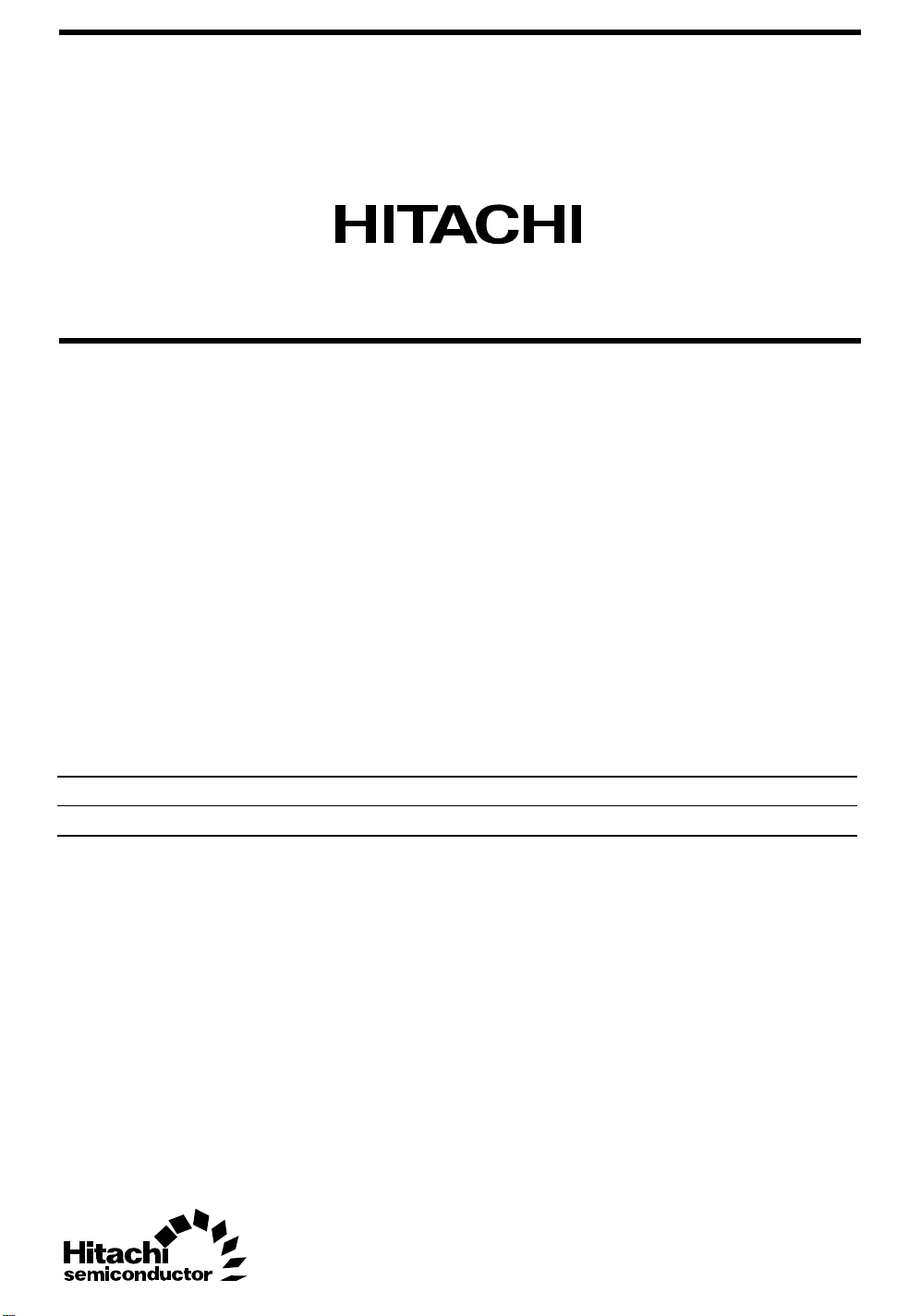
HD74LVC14
Pin Arrangement
1A
1Y
2A
2Y
3A
3Y
GND
1
2
3
4
5
6
7
14
13
12
11
10
V
CC
6A
6Y
5A
5Y
4A
9
8
4Y
(Top view)
Absolute Maximum Ratings
Item Symbol Ratings Unit Conditions
Supply voltage range V
Input diode current I
Input voltage V
Output diode current I
Output voltage V
Output current I
VCC, GND current / pin ICC or I
CC
IK
I
OK
O
O
GND
Storage temperature Tstg –65 to +150 °C
Note: The absolute maximum ratings are values which must not individually be exceeded, and furthermore,
no two of which may be realized at the same time.
–0.5 to 6.0 V
–50 mA VI = –0.5 V
–0.5 to 6.0 V
–50 mA VO = –0.5 V
50 mA VO = VCC+0.5 V
–0.5 to VCC+0.5 V
±50 mA
100 mA
2
HD74LVC14
Recommended Operating Conditions
Item Symbol Ratings Unit Conditions
Supply voltage V
Input / Output voltage V
CC
I
V
O
Operating temperature Ta –40 to 85 °C
Output current I
Input rise / fall time
*1
OH
I
OL
tr, t
f
Notes: 1. This item guarantees maximum limit when one input switches.
Waveform : Refer to test circuit of switching characteristics.
2. duty cycle ≤ 50%
1.5 to 5.5 V Data retention
2.0 to 5.5 V At operation
0 to 5.5 V A
0 to V
CC
VY
–12 mA VCC = 2.7 V
*2
–24
mA VCC = 3.0 V to 5.5 V
12 mA VCC = 2.7 V
*2
24
mA VCC = 3.0 V to 5.5 V
10 ns/V
3
 Loading...