

HIT HD74LVC139 Datasheet
HD74LVC139
Dual 2-to-4-line Decoders / Demultiplexers
ADE-205-069B(Z)
Rev.2
September 1995
Description
The HD74LVC139 has two independent two-to-four-line decoders each with a single active low enable
input in a 16 pin package. Data on the select inputs cause one of the four normally high outputs to go low.
Low voltage and high speed operation is suitable at the battery drive product (note type personal computer)
and low power consumption extends the life of a battery for long time operation.
Features
• VCC = 2.0 V to 5.5 V
• All inputs VIH (Max.) = 5.5 V (@VCC = 0 V to 5.5 V)
• Typical VOL ground bounce < 0.8 V (@VCC = 3.3 V, Ta = 25°C)
• Typical VOH undershoot > 2.0 V (@VCC = 3.3 V, Ta = 25°C)
• High output current ±24 mA (@VCC = 3.0 V to 5.5 V)
Function Table
Input
Enable Select Outputs
GB AY
H X X HHHH
LLLLHHH
LLHHLHH
LHLHHLH
L H H HHHL
H : High level
L : Low level
X : Immaterial
0
Y
1
Y
2
Y
3
HD74LVC139
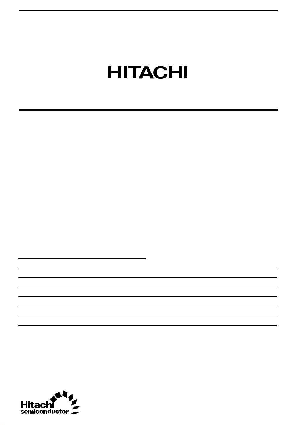
Pin Arrangement
1G
1A
1B
1Y
1Y
1Y
1Y
GND
1
2
3
4
0
5
1
6
2
7
3
G
A
B
Y
0
Y
1
Y
2
Y
3
G
A
B
Y
0
Y
1
Y
2
Y
3
8
16
15
14
13
12
11
10
V
CC
2G
2A
2B
2Y
0
2Y
1
2Y
2
9
2Y
3
(Top view)
Absolute Maximum Ratings
Item Symbol Ratings Unit Conditions
Supply voltage V
Input diode current I
Input voltage V
Output diode current I
Output voltage V
Output current I
VCC, GND current / pin I
IK
OK
O
CC
CC
I
O
or I
Storage temperature Tstg –65 to 150 °C
Note: The absolute maximum ratings are values which must not individually be exceeded, and furthermore,
no two of which may be realized at the same time.
–0.5 to 6.0 V
–50 mA VI = –0.5 V
–0.5 to 6.0 V
–50 mA VO = –0.5 V
50 mA VO = V
–0.5 to V
+0.5 V
CC
±50 mA
100 mA
GND
+0.5 V
CC
2
HD74LVC139
Recommended Operating Conditions
Item Symbol Ratings Unit Conditions
Supply voltage V
Input / output voltage V
CC
I
V
O
Operating temperature Ta –40 to 85 °C
Output current I
Input rise / fall time
*1
OH
I
OL
tr, t
f
Notes: 1. This item guarantees maximum limit when one input switches.
Waveform : Refer to test circuit of switching characteristics.
2. duty cycle ≤ 50%
1.5 to 5.5 V Data retention
2.0 to 5.5 V At operation
0 to 5.5 V G, A, B
0 to V
CC
VY
to Y
0
3
–12 mA VCC = 2.7 V
*2
–24
mA VCC = 3.0 V to 5.5 V
12 mA VCC = 2.7 V
*2
24
mA VCC = 3.0 V to 5.5 V
10 ns/V
Electrical Characteristics
Item Symbol V
Input voltage V
Output voltage V
Input current I
Quiescent supply current I
V
V
∆I
IH
IL
OH
OL
IN
CC
CC
Ta = –40 to 85°C
(V) Min Max Unit Test Conditions
CC
2.7 to 3.6 2.0 — V
4.5 to 5.5 VCC×0.7 — V
2.7 to 3.6 — 0.8 V
4.5 to 5.5 — VCC×0.3 V
2.7 to 5.5 V
–0.2 — V IOH = –100 µA
CC
2.7 2.2 — V IOH = –12 mA
3.0 2.4 — V
3.0 2.0 — V IOH = –24 mA
4.5 3.8 — V
2.7 to 5.5 — 0.2 V IOL = 100 µA
2.7 — 0.4 V IOL = 12 mA
3.0 — 0.55 V IOL = 24 mA
4.5 — 0.55 V
0 to 5.5 — ±5.0 µAVIN = 5.5 V or GND
5.5 — 20 µAVIN = VCC or GND
3.0 to 3.6 — 500 µAVIN = one input at (V
other inputs at V
CC
–0.6)V,
CC
or GND
3
 Loading...