

HIT HD74LVC138 Datasheet

HD74LVC138
3-to-8-line Decoder / Demultiplexer
ADE-205-068B(Z)
Rev.2
September 1995
Description
The HD74LVC138 has three binary select inputs in a 16 pin package. If the device is enabled these inputs
determine which one of the eight normally high outputs will go low. Two active low and one active high
enables are provided to ease the cascading of decoders. Low voltage and high speed operation is suitable at
the battery drive product (note type personal computer) and low power consumption extends the life of a
battery for long time operation.
Features
• VCC = 2.0 V to 5.5 V
• All inputs VIH (Max.) = 5.5 V (@VCC = 0 V to 5.5 V)
• Typical VOL ground bounce < 0.8 V (@VCC = 3.3 V, Ta = 25°C)
• Typical VOH undershoot > 2.0 V (@VCC = 3.3 V, Ta = 25°C)
• High output current ±24 mA (@VCC = 3.0 V to 5.5 V)
HD74LVC138
Function Table
Inputs
Enable Select Outputs
G
XXHXXXHHHHHHHH
XHXXXXHHH HH HH H
L XXXXXHHHHHHHH
HLLLLLLHHHHHHH
HLLLLHHLHHHHHH
HLLLHLHHL HHHHH
HLLLHHHHHL HHHH
HLLHLLHHHHLHHH
HLLHLHHHHHHLHH
HLLHHLHHHHHHLH
HLLHHHHHHHHHHL
H : High level
L : Low level
X : Immaterial
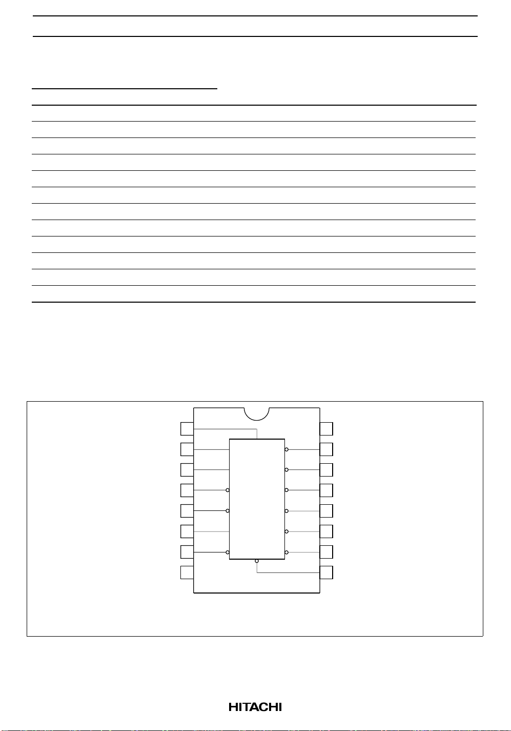
G
1
G
2A
CBAY0Y1Y2Y3Y4Y5Y6Y
2B
7
Pin Arrangement
G
2A
G
2B
G
Y
GND
1
A
2
B
3
C
4
5
6
1
7
7
A
B
C
G
2A
G
2B
G
1
Y
7
Y
0
Y
1
Y
2
Y
3
Y
4
Y
Y
6
5
8
16
15
14
13
12
11
10
V
CC
Y
0
Y
1
Y
2
Y
3
Y
4
Y
5
Y
9
6
(Top view)
2
HD74LVC138
Absolute Maximum Ratings
Item Symbol Ratings Unit Conditions
Supply voltage V
Input diode current I
Input voltage V
Output diode current I
Output voltage V
Output current I
VCC, GND current / pin I
IK
OK
O
CC
CC
I
O
or I
GND
Storage temperature Tstg –65 to +150 °C
Note: The absolute maximum ratings are values which must not individually be exceeded, and furthermore,
no two of which may be realized at the same time.
Recommended Operating Conditions
–0.5 to 6.0 V
–50 mA VI = –0.5 V
–0.5 to 6.0 V
–50 mA VO = –0.5 V
50 mA VO = V
+0.5 V
CC
–0.5 to VCC +0.5 V
±50 mA
100 mA
Item Symbol Ratings Unit Conditions
Supply voltage V
CC
1.5 to 5.5 V Data retention
2.0 to 5.5 V At operation
Input / output voltage V
I
V
O
0 to 5.5 V G, A, B, C
0 to V
CC
VY
0 to Y7
Operating temperature Ta –40 to 85 °C
Output current I
Input rise / fall time
*1
OH
I
OL
tr, t
f
–12 mA VCC = 2.7 V
*2
–24
mA VCC = 3.0 V to 5.5 V
12 mA VCC = 2.7 V
*2
24
mA VCC = 3.0 V to 5.5 V
10 ns/V
Notes: 1. This item guarantees maximum limit when one input switches.
Waveform : Refer to test circuit of switching characteristics.
2. duty cycle ≤ 50%
3
 Loading...