


HD74LV595A
8-bit Shift Registers with 3-state Outputs
ADE-205-281 (Z)
1st Edition
April 1999
Description
This device each contains an 8-bit serial-in, parallel-out shift registers that feeds an 8-bit D-type storage
register. The storage register has parallel 3-state outputs. Separate clocks are provided for both the shift
register anf the storage register. The shift register has a direct-overriding clear, serial input, and serial
output pins for cascading.
Both the shift register anf the storage register clocks are positive-edge triggered. If the user wishes to
connect both clocks together, the shift register state will always be one clock pulse ahead of the storage
register. Low-voltage and high-speed operation is suitable for the battery-powered products (e.g., notebook
computers), and the low-power consumption extends the battery life.
Features
• VCC = 2.0 V to 5.5 V operation
• All inputs VIH (Max.) = 5.5 V (@VCC = 0 V to 5.5 V)
• All outputs VO (Max.) = 5.5 V (@VCC = 0 V)
• Typical VOL ground bounce < 0.8 V (@VCC = 3.3 V, Ta = 25°C)
• Typical VOH undershoot > 2.3 V (@VCC = 3.3 V, Ta = 25°C)
• Output current ±6 mA (@VCC = 3.0 V to 3.6 V), ±12 mA (@VCC = 4.5 V to 5.5 V)

HD74LV595A
Function Table
Inputs
SER SRCLK SRCLR RCLK G Function
X XXXHForce outputs into high-impedance state
X XXXLEnable paralle output
X X L X X Reset shift register
L ↑ H X X Shift data into shift register
H ↑ H X X Shift data into shift register
X ↓ H X X Shift register remains unchanged
XXX↑ X Transfer shift register contents to latch
register
XXX↓ X Latch register remains unchanged
Note: H: High level
L: Low level
X: Immaterial
↑: Low to high transition
↓: High to low transition
2
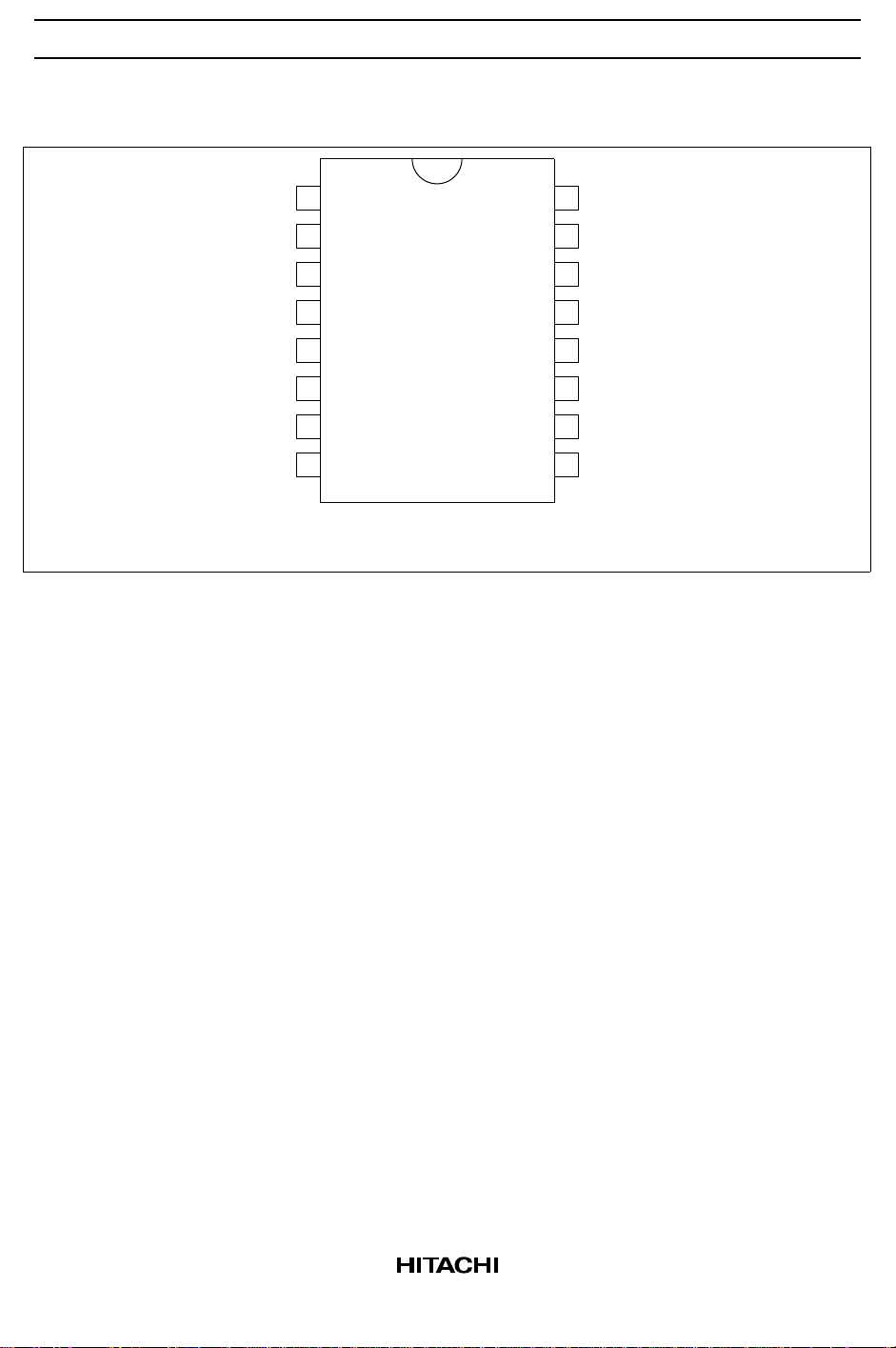
Pin Arrangement
HD74LV595A
V
1
Q
B
16
CC
Q
Q
Q
Q
Q
Q
GND
2
C
3
D
4
E
5
F
6
G
7
H
8
15
14
13
12
11
10
9
Q
A
SER
G
RCLK
SRCLK
SRCLR
Q
H'
(Top view)
3
HD74LV595A
Absolute Maximum Ratings
Item Symbol Ratings Unit Conditions
Supply voltage range V
Input voltage range*
Output voltage range*
1
1, 2
Input clamp current I
Output clamp current I
Continuous output current I
Continuous current through
V
or GND
CC
Maximum power dissipation
at Ta = 25°C (in still air)*
3
CC
V
I
V
O
IK
OK
O
or I
I
CC
GND
P
T
Storage temperature Tstg –65 to 150 °C
Notes: The absolute maximum ratings are values which must not individually be exceeded, and furthermore,
no two of which may be realized at the same time.
1. The input and output voltage ratings may be exceeded if the input and output clamp-current
ratings are observed.
2. This value is limited to 5.5 V maximum.
3. The maximum package power dissipation was calculated using a junction temperature of 150°C.
–0.5 to 7.0 V
–0.5 to 7.0 V
–0.5 to VCC + 0.5 V Output: H or L
–0.5 to 7.0 Output: Z or VCC: OFF
–20 mA VI < 0
±50 mA VO < 0 or VO > V
±25 mA VO = 0 to V
CC
CC
±70 mA
785 mW SOP
500 TSSOP
4
HD74LV595A
Recommended Operating Conditions
Item Symbol Min Max Unit Conditions
Supply voltage range V
Input voltage range V
Output voltage range V
Output current I
CC
I
O
OH
I
OL
Input transition rise or fall rate ∆t /∆v 0 200 ns/V VCC = 2.3 to 2.7 V
Operating free-air temperature Ta –40 85 °C
Note: Unused or floating inputs must be held high or low.
2.0 5.5 V
0 5.5 V
0VCCV H or L
0 5.5 High impedance state
— –50 µAV
—–2 mAV
—–6 V
= 2.0 V
CC
= 2.3 to 2.7 V
CC
= 3.0 to 3.6 V
CC
— –12 VCC = 4.5 to 5.5 V
—50 µAV
= 2.0 V
CC
— 2 mA VCC = 2.3 to 2.7 V
—6 V
—12 V
= 3.0 to 3.6 V
CC
= 4.5 to 5.5 V
CC
0 100 VCC = 3.0 to 3.6 V
020 V
= 4.5 to 5.5 V
CC
5
HD74LV595A
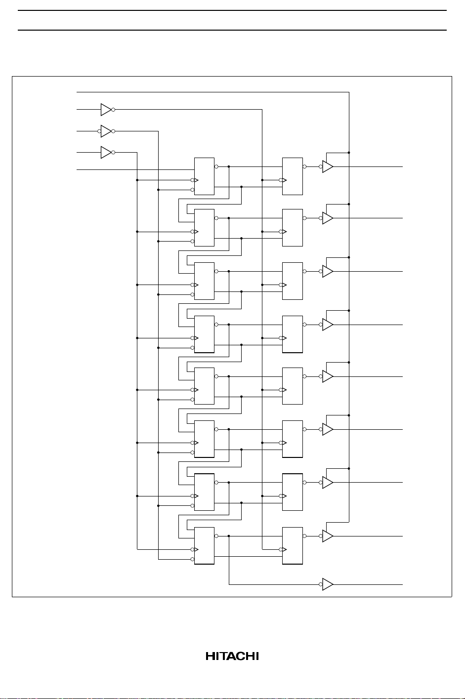
Logic Diagram
(13)
G
(12)
RCLK
SER
(10)
(11)
(14)
SRCLR
SRCLK
1D
R
C1
3R
3S
C3
(15)
Q
A
2S
2R
R
2S
2R
R
2S
2R
R
2S
2R
R
2S
2R
R
2S
2R
R
C2
C2
C2
C2
C2
C2
3R
3S
3R
3S
3R
3S
3R
3S
3R
3S
3R
3S
C3
C3
C3
C3
C3
C3
(1)
(2)
(3)
(4)
(5)
(6)
Q
B
Q
C
Q
D
Q
E
Q
F
Q
G
2S
2R
R
C2
3R
3S
C3
(7)
(9)
Q
H
Q
'
H
6

Timing Diagram
SRCLK
SER
RCLK
SRCLR
G
Q
A
Q
B
Q
C
Q
D
Q
E
Q
F
Q
G
Q
H
Q
H'
HD74LV595A
SHIFT
HIGH IMPEDANCE CLEAR
7

HD74LV595A
DC Electrical Characteristics
• Ta = –40 to 85°C
Item Symbol VCC (V)* Min Typ Max Unit Test Conditions
Input voltage V
Output voltage V
Input current I
Off-state
IH
V
IL
OH
V
OL
IN
I
OZ
output current
Quiescent
I
CC
supply current
Output leakage
I
OFF
current
Input
C
IN
capacitance
Note: For conditions shown as Min or Max, use the appropriate values under recommended operating
conditions.
2.0 1.5 — — V
2.3 to 2.7 VCC × 0.7 — —
3.0 to 3.6 VCC × 0.7 — —
4.5 to 5.5 VCC × 0.7 — —
2.0 — — 0.5
2.3 to 2.7 — — VCC × 0.3
3.0 to 3.6 — — VCC × 0.3
4.5 to 5.5 — — VCC × 0.3
Min to
VCC – 0.1 — — V IOH = –50 µA
Max
2.3 2.0 — — IOH = –2 mA
3.0 2.48 — — IOH = –6 mA
4.5 3.8 — — IOH = –12 mA
Min to
— — 0.1 IOL = 50 µA
Max
2.3 — — 0.4 IOL = 2 mA
3.0 — — 0.44 IOL = 6 mA
4.5 — — 0.55 IOL = 12 mA
0 to 5.5 — — ±1 µAVIN = 5.5 V or GND
5.5 — — ±5 µAVO = VCC or GND
5.5 — — 20 µAVIN = VCC or GND, IO = 0
0——5 µAVI or VO = 0 to 5.5 V
3.3 — 3.5 — pF VI = VCC or GND
8

Switching Characteristics
• VCC = 2.5 ± 0.2 V
Ta = 25°C Ta = –40 to 85°C
Test
Item Symbol Min Typ Max Min Max Unit
Maximum f
clock
max
65 80 — 45 — MHz CL = 15 pF
60 70 — 40 — CL = 50 pF
frequency
Propagation t
PLH/tPHL
— 11.6 16.4 1.0 19.5 ns CL = 15 pF SRCLK QH'
delay time — 14.8 19.4 1.0 22.5 CL = 50 pF
— 10.5 15.3 1.0 18.0 CL = 15 pF RCLK QA – Q
— 13.7 18.3 1.0 21.0 CL = 50 pF
t
PHL
— 11.2 16.2 1.0 18.2 CL = 15 pF SRCLK QH'
— 14.4 19.2 1.0 21.2 CL = 50 pF
Enable time t
Disable time t
Setup time t
ZH
t
ZL
HZ
t
LZ
SU
— 10.3 14.8 1.0 17.5 ns CL = 15 pF G QA – Q
— 12.2 17.7 1.0 20.5 CL = 50 pF
— 7.6 11.5 1.0 13.5 ns CL = 15 pF
— 14.4 18.2 1.0 19.2 CL = 50 pF
5.5 — — 5.5 — ns SER before SRCLK ↑
10.0 — — 10.5 — SRCLK ↑ before
10.0 — — 11.0 — SRCLR low before
5.0 — — 5.0 — SRCLR high
Hold time t
h
2.0 — — 2.0 — ns SER after SRCLK ↑
0.5 — — 0.5 — SRCLK ↑ after
0.5 — — 0.5 — SRCLR low after
Pulse width t
w
7.0 — — 7.5 — ns RCLK high or low
7.0 — — 7.5 — SRCLK high or low
6.0 — — 6.5 — SRCLR low
Conditions
HD74LV595A
FROM
(Input)TO(Output)
H
H
RCLK ↑
RCLK ↑
(inactive) before
SRCLK ↑
RCLK ↑
RCLK ↑
9

HD74LV595A
• VCC = 3.3 ± 0.3 V
Ta = 25°C Ta = –40 to 85°C
Test
Item Symbol Min Typ Max Min Max Unit
Maximum f
clock
max
80 150 — 70 — MHz CL = 15 pF
55 130 — 50 — CL = 50 pF
frequency
Propagation t
PLH/tPHL
— 8.8 13.0 1.0 15.0 ns CL = 15 pF SRCLK QH'
delay time — 11.3 16.5 1.0 18.5 CL = 50 pF
— 7.7 11.9 1.0 13.5 CL = 15 pF RCLK QA – Q
— 10.2 15.4 1.0 17.0 CL = 50 pF
t
PHL
— 8.4 12.8 1.0 13.7 CL = 15 pF SRCLK QH'
— 10.9 16.3 1.0 17.2 CL = 50 pF
Enable time t
Disable time t
Setup time t
ZH
t
ZL
HZ
t
LZ
SU
— 7.5 11.5 1.0 13.5 ns CL = 15 pF G QA – Q
— 9.0 15.0 1.0 17.0 CL = 50 pF
— 5.9 11.7 1.0 13.5 ns CL = 15 pF
— 12.1 15.7 1.0 16.2 CL = 50 pF
3.5 — — 3.5 — ns SER before SRCLK ↑
8.0 — — 8.5 — SRCLK ↑ before RCLK ↑
8.0 — — 9.0 — SRCLR low before RCLK
3.0 — — 3.0 — SRCLR high (inactive)
Hold time t
h
1.5 — — 1.5 — ns SER after SRCLK ↑
0.0 — — 0.0 — SRCLK ↑ after RCLK ↑
0.0 — — 0.0 — SRCLR low after RCLK ↑
Pulse width t
w
5.0 — — 5.0 — ns RCLK high or low
5.0 — — 5.0 — SRCLK high or low
5.0 — — 5.0 — SRCLR low
Conditions
FROM
(Input)
↑
before SRCLK ↑
TO
(Output)
H
H
10

Switching Characteristics (cont)
• VCC = 5.0 ± 0.5 V
Ta = 25°C Ta = –40 to 85°C
Test
Item Symbol Min Typ Max Min Max Unit
Maximum f
clock
max
135 185 — 115 — MHz CL = 15 pF
95 155 — 85 — CL = 50 pF
frequency
Propagation t
PLH/tPHL
— 6.2 8.2 1.0 9.4 ns CL = 15 pF SRCLK QH'
delay time — 7.7 10.2 1.0 11.4 CL = 50 pF
— 5.4 7.4 1.0 8.5 CL = 15 pF RCLK QA – Q
— 6.9 9.4 1.0 10.5 CL = 50 pF
t
PHL
— 5.9 8.0 1.0 9.1 CL = 15 pF SRCLK QH'
— 7.4 10.0 1.0 11.1 CL = 50 pF
Enable time t
Disable time t
Setup time t
ZH
t
ZL
HZ
t
LZ
SU
— 4.8 8.6 1.0 10.0 ns CL = 15 pF G QA – Q
— 8.3 10.6 1.0 12.0 CL = 50 pF
— 4.8 8.6 1.0 10.0 ns CL = 15 pF
— 7.6 11.0 1.0 11.0 CL = 50 pF
3.0 — — 3.0 — ns SER before SRCLK ↑
5.0 — — 5.0 — SRCLK ↑ before RCLK ↑
5.0 — — 5.0 — SRCLR low before RCLK ↑
2.5 — — 2.5 — SRCLR high (inactive)
Hold time t
h
2.0 — — 2.0 — ns SER after SRCLK ↑
0.0 — — 0.0 — SRCLK ↑ after RCLK ↑
0.0 — — 0.0 — SRCLR low after RCLK ↑
Pulse width t
w
5.0 — — 5.0 — ns RCLK high or low
5.0 — — 5.0 — SRCLK high or low
5.0 — — 5.0 — SRCLR low
Conditions
HD74LV595A
FROM
(Input)
before SRCLK ↑
TO
(Output)
H
H
11

HD74LV595A
Output-skew Characteristics
• CL = 50 pF
Ta = 25°C Ta = –40 to 85°C
Item Symbol V
Output skew t
sk (O)
Note: Skew between any outputs of the same package switching in the same direction. This parameter is
warranted but not production tested.
Operating Characteristics
• CL = 50 pF
Item Symbol V
Power
dissipation
capacitance
C
PD
= (V) Min Max Min Max Unit
CC
2.3 to 2.7 — 2.0 — 2.0 ns
3.0 to 3.6 — 1.5 — 1.5
4.5 to 5.5 — 1.0 — 1.0
Ta = 25°C
= (V) Min Typ Max Unit Test Conditions
CC
3.3 — 32.7 — pF f = 10 MHz
5.0 — 33.1 —
Noise Characteristics
• CL = 50 pF
Item Symbol V
Quiet output,
maximum
dynamic V
Quiet output,
minimum
dynamic V
Quiet output,
minimum
dynamic V
High-level
dynamic
input voltage
Low-level
dynamic
inout voltage
V
OL (P)
OL
V
OL (V)
OL
V
OH (V)
OH
V
IH (D)
V
IL (D)
Ta = 25°C
= (V) Min Typ Max Unit Test Conditions
CC
3.3 — 0.65 0.8 V
3.3 — –0.59 –0.8
3.3 — 2.84 —
3.3 2.31 — —
3.3 — — 0.99
12

Test Circuit
Output
C
HD74LV595A
Ω
1 K
S2
L
OPEN
GND
V
CC
TEST
t / t
PLH PHL
t / t
ZH HZ
t / t
ZL LZ
Note: C includes the probe and jig capacitance.
L
S2
OPEN
GND
V
CC
13

HD74LV595A
Waveform – 1
SRCLK
Waveform – 2
SRCLR
Q
H'
Q
50% V
H'
90%
10%
10%
CC
t
90%
50% V
t
PHL
r
CC
t
f
V
CC
GND
t
w
1/f
max
t
PLH
t
TLH
50% V
t
PHL
t
THL
t
w
V
CC
CC
GND
50% V
CC
SRCLK
Waveform – 3
RCLK
Q
A-QH
50% V
CC
t
PLH/tPHL
50% V
CC
t
su
50% V
CC
V
CC
GND
V
CC
GND
14

Waveform – 4
G
Waveform – A
Waveform – B
Waveform – 5
SRCLK
SER
t
f
t
r
90 % 90 %
50 % V
CC
50 % V
10 % 10 %
t
ZL
50 % V
CC
t
ZH
50 % V
CC
t
LZ
t
HZ
Valid
50% V
CC
t
su
t
h
50% V
CC
CC
V + 0.3 V
V – 0.3 V
V
GND
V
GND
CC
CC
OL
OH
HD74LV595A
V
CC
0 V
V
CC
V
OL
V
OH
0 V
Waveform – 6
SRCLK
Notes:
1. Input waveform: PRR ≤ 1 MHz, Zo = 50 Ω, t ≤ 3 ns, t ≤ 3 ns
2. Waveform-A is for an output with internal conditions such that the output is low except when disabled
by the output control.
3. Waveform-B is for an output with internal conditions such that the output is high except when disabled
by the output control.
4. The output are measured one at a time with one transition per measurement.
RCLK
V
CC
50% V
CC
GND
t
su
50%
V
CC
t
w
V
CC
GND
15

HD74LV595A
Package Dimensions
16
10.06
10.5 Max
9
5.5
1
0.80 Max
1.27
0.42 ± 0.08
± 0.06
0.40
Dimension including the plating thickness
Base material dimension
8
0.12
0.10 ± 0.10
0.15
M
2.20 Max
7.80
0.22 ± 0.05
0.20 ± 0.04
0.70 ± 0.20
Hitachi Code
JEDEC
EIAJ
Weight
(reference value)
+ 0.20
– 0.30
1.15
0
° – 8°
FP-16DA
—
Conforms
0.24 g
16

16
HD74LV595A
Unit: mm
9.9
10.3 Max
9
1
1.27
0.635 Max
*0.42 ± 0.08
0.40 ± 0.06
*Dimension including the plating thickness
Base material dimension
8
0.25
+ 0.11
– 0.04
0.14
0.15
3.95
1.75 Max
M
6.10
1.08
0.20 ± 0.03
*0.22 ± 0.03
+ 0.67
0.60
– 0.20
Hitachi Code
JEDEC
EIAJ
Weight
+ 0.10
– 0.30
0° – 8°
(reference value)
FP-16DN
Conforms
Conforms
0.15 g
17

HD74LV595A
0.22
0.20 ± 0.06
5.0
5.3 Max
16 9
4.40
18
0.65
+ 0.08
– 0.07
0.13
0.65 Max
1.0
M
6.40 ± 0.20
0.10
1.10 Max
Dimension including the plating thickness
Base material dimension
0.17 ± 0.05
0.15 ± 0.04
+0.03
–0.04
0.07
0° – 8°
Hitachi Code
JEDEC
EIAJ
Weight
(reference value)
0.50 ± 0.10
TTP-16DA
—
—
0.05 g
18

Cautions
1. Hitachi neither warrants nor grants licenses of any rights of Hitachi’s or any third party’s patent,
copyright, trademark, or other intellectual property rights for information contained in this document.
Hitachi bears no responsibility for problems that may arise with third party’s rights, including
intellectual property rights, in connection with use of the information contained in this document.
2. Products and product specifications may be subject to change without notice. Confirm that you have
received the latest product standards or specifications before final design, purchase or use.
3. Hitachi makes every attempt to ensure that its products are of high quality and reliability. However,
contact Hitachi’s sales office before using the product in an application that demands especially high
quality and reliability or where its failure or malfunction may directly threaten human life or cause risk
of bodily injury, such as aerospace, aeronautics, nuclear power, combustion control, transportation,
traffic, safety equipment or medical equipment for life support.
4. Design your application so that the product is used within the ranges guaranteed by Hitachi particularly
for maximum rating, operating supply voltage range, heat radiation characteristics, installation
conditions and other characteristics. Hitachi bears no responsibility for failure or damage when used
beyond the guaranteed ranges. Even within the guaranteed ranges, consider normally foreseeable
failure rates or failure modes in semiconductor devices and employ systemic measures such as failsafes, so that the equipment incorporating Hitachi product does not cause bodily injury, fire or other
consequential damage due to operation of the Hitachi product.
5. This product is not designed to be radiation resistant.
6. No one is permitted to reproduce or duplicate, in any form, the whole or part of this document without
written approval from Hitachi.
7. Contact Hitachi’s sales office for any questions regarding this document or Hitachi semiconductor
products.
Hitachi, Ltd.
Semiconductor & Integrated Circuits.
Nippon Bldg., 2-6-2, Ohte-machi, Chiyoda-ku, Tokyo 100-0004, Japan
Tel: Tokyo (03) 3270-2111 Fax: (03) 3270-5109
URL NorthAmerica : http:semiconductor.hitachi.com/
For further information write to:
Hitachi Semiconductor
(America) Inc.
179 East Tasman Drive,
San Jose,CA 95134
Tel: <1> (408) 433-1990
Fax: <1>(408) 433-0223
Europe : http://www.hitachi-eu.com/hel/ecg
Asia (Singapore) : http://www.has.hitachi.com.sg/grp3/sicd/index.htm
Asia (Taiwan) : http://www.hitachi.com.tw/E/Product/SICD_Frame.htm
Asia (HongKong) : http://www.hitachi.com.hk/eng/bo/grp3/index.htm
Japan : http://www.hitachi.co.jp/Sicd/indx.htm
Hitachi Europe GmbH
Electronic components Group
Dornacher Stra§e 3
D-85622 Feldkirchen, Munich
Germany
Tel: <49> (89) 9 9180-0
Fax: <49> (89) 9 29 30 00
Hitachi Europe Ltd.
Electronic Components Group.
Whitebrook Park
Lower Cookham Road
Maidenhead
Berkshire SL6 8YA, United Kingdom
Tel: <44> (1628) 585000
Fax: <44> (1628) 778322
Hitachi Asia Pte. Ltd.
16 Collyer Quay #20-00
Hitachi Tower
Singapore 049318
Tel: 535-2100
Fax: 535-1533
Hitachi Asia Ltd.
Taipei Branch Office
3F, Hung Kuo Building. No.167,
Tun-Hwa North Road, Taipei (105)
Tel: <886> (2) 2718-3666
Fax: <886> (2) 2718-8180
Copyright ' Hitachi, Ltd., 1999. All rights reserved. Printed in Japan.
Hitachi Asia (Hong Kong) Ltd.
Group III (Electronic Components)
7/F., North Tower, World Finance Centre,
Harbour City, Canton Road, Tsim Sha Tsui,
Kowloon, Hong Kong
Tel: <852> (2) 735 9218
Fax: <852> (2) 730 0281
Telex: 40815 HITEC HX
 Loading...