

HIT HD74LV4066A Datasheet

HD74LV4066A
Quad. Analog Switches / Quad. Multiplexers
ADE-205-285 (Z)
1st Edition
April 1999
Description
The HD74LV4066A handles both analog and digital signals, and enables signals of either type with
amplitudes of up to 5.5 V (peak) to be transmitted in either direction (at VCC = 0 V to 5.5 V).
Each switch section has its own enable input control (C). A high-level voltage applied to C turns on the
associated switch section.
Applications include signal gating, chopping, modulation or demodulation (modem), and signal
multiplexing for analog-to-digital and digital-to-analog conversion systems.
Features
• VCC = 2.0 V to 5.5 V operation
• All inputs VIH (Max.) = 5.5 V (@VCC = 0 V to 5.5 V)
Function Table
Control Switch
L OFF
HON
Note: H: High level
L: Low level
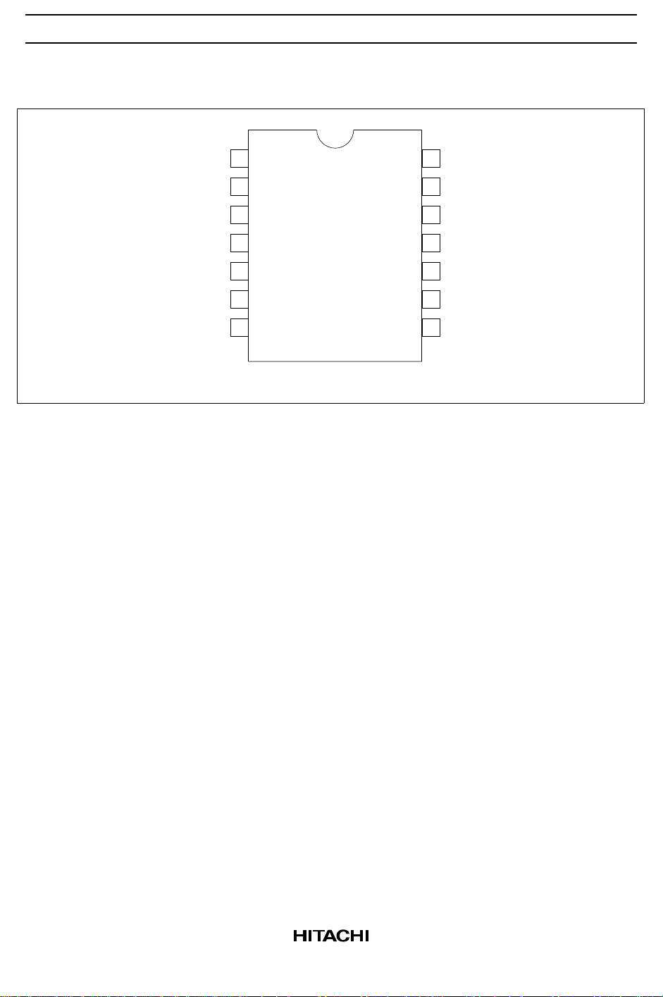
HD74LV4066A
Pin Arrangement
1A
1B
2B
2A
2C
3C
GND
1
2
3
4
5
6
7
(Top view)
14
13
12
11
10
V
CC
1C
4C
4A
4B
9
3B
3A
8
2
HD74LV4066A
Absolute Maximum Ratings
Item Symbol Ratings Unit Conditions
Supply voltage range V
Input voltage range*
Output voltage range*
1
1, 2
Input clamp current I
Output clamp current I
Continuous output current I
Continuous current through
V
or GND
CC
Maximum power dissipation
at Ta = 25°C (in still air)*
3
CC
V
I
V
O
IK
OK
O
or I
I
CC
GND
P
T
Storage temperature Tstg –65 to 150 °C
Notes: The absolute maximum ratings are values which must not individually be exceeded, and furthermore,
no two of which may be realized at the same time..
1. The input and output voltage ratings may be exceeded even if the input and output clamp-current
ratings are observed.
2. This value is limited to 5.5 V maximum.
3. The maximum package power dissipation was calculated using a junction temperature of 150°C.
–0.5 to 7.0 V
–0.5 to 7.0 V
–0.5 to VCC + 0.5 V Output: H or L
–20 mA VI < 0
±50 mA VO < 0 or VO > V
±25 mA VO = 0 to V
CC
±50 mA
785 mW SOP
500 TSSOP
CC
Recommended Operating Conditions
Item Symbol Min Max Unit Conditions
1
Supply voltage range V
Input voltage range V
Output voltage range V
CC
I
I/O
2.0*
0 5.5 V
0VCCV
Input transition rise or fall rate ∆t/∆v 0 200 ns/V VCC = 2.3 to 2.7 V
0 100 VCC = 3.0 to 3.6 V
020 V
Operating free-air temperature Ta –40 85 °C
Notes: Unused or floating inputs must be held high or low.
1. With the supply voltage at or around 2 V, the analog switch on-state resistance loses linearity
significantly. It is recommended that only digital signals be transmitted at these low supply
voltages.
5.5 V
= 4.5 to 5.5 V
CC
3
HD74LV4066A
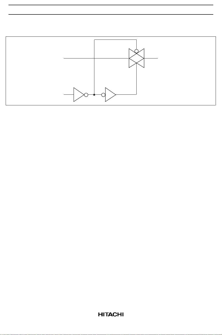
Logic Diagram
A
C
B
4

HD74LV4066A
OU
DC Electrical Characteristics
Ta = 25°C Ta = –40 to 85°C
Item Symbol VCC (V) Min Typ Max Min Max Unit Test Conditions
Input voltage V
On-state
IH
V
IL
R
ON
switch
resistance
Peak on
R
ON (P)
resistance
Difference of
∆R
ON
on-state
resistance
between
switches
Off-state
Is (OFF) 5.5 — — ±0.1 — ±1.0 µAVIN = VCC, V
switch leakage
current
On-state
Is (ON) 5.5 — — ±0.1 — ±1.0 µAVIN = VCC or GND
switch leakage
current
Input current I
Quiescent
IN
I
CC
supply current
Note: For conditions shown as Min or Max use the appropriate values under recommended operating
conditions.
2.0 — — — 1.5 — V
2.3 to 2.7 — — — V
3.0 to 3.6 — — — V
4.5 to 5.5 — — — V
× 0.7 —
CC
× 0.7 —
CC
× 0.7 —
CC
2.0 — — — — 0.5
2.3 to 2.7 — — — — V
3.0 to 3.6 — — — — V
4.5 to 5.5 — — — — V
CC
CC
CC
× 0.3
× 0.3
× 0.3
2.3 — 60 180 — 225 Ω VIN = VCC or GND
VC = V
IH
IT = 1 mA
3.0 — 50 150 — 190
4.5 — 40 75 — 100
2.3 — 250 500 — 600 Ω VIN = VCC to GND
VC = V
IH
IT = 1 mA
3.0 — 100 180 — 225
4.5 — 50 100 — 125
2.3 — 20 30 — 40 Ω VIN = VCC to GND
VC = V
IH
IT = 1 mA
3.0 — 10 20 — 30
4.5 — 7 15 — 20
=
T
GND or VIN = GND,
VO = VCC, VC = V
VC = V
IH
0 to 5.5 — — ±0.1 — ±1.0 µAVIN = 5.5 V or GND
5.5 — — — — 20 µAVIN = VCC or GND
IL
5
HD74LV4066A
Switching Characteristics
• VCC = 2.5 ± 0.2 V
Ta = 25°C Ta = –40 to 85°C
Item Symbol Min Typ Max Min Max Unit Test Conditions
Propagation
delay time
Enable time t
Disable
time
• VCC = 3.3 ± 0.3 V
Item Symbol Min Typ Max Min Max Unit Test Conditions
Propagation
delay time
Enable time t
Disable
time
t
PLH
t
PHL
— 2.0 10.0 — 16.0 ns CL = 15 pF A or B B or A
— 5.0 12.0 — 18.0 CL = 50 pF
ZH
t
ZL
— 6.0 15.0 — 20.0 ns RL = 1 kΩ CL = 15 pF C A or B
— 8.0 25.0 — 32.0 CL = 50 pF
t
HZ
t
LZ
— 7.0 15.0 — 23.0 ns RL = 1 kΩ CL = 15 pF C A or B
— 11.0 25.0 — 32.0 CL = 50 pF
Ta = 25°C Ta = –40 to 85°C
t
PLH
t
PHL
— 1.5 6.0 — 10.0 ns CL = 15 pF A or B B or A
— 4.0 9.0 — 12.0 CL = 50 pF
ZH
t
ZL
— 4.0 11.0 — 15.0 ns RL = 1 kΩ CL = 15 pF C A or B
— 6.0 18.0 — 22.0 CL = 50 pF
t
HZ
t
LZ
— 5.0 11.0 — 15.0 ns RL = 1 kΩ CL = 15 pF C A or B
— 8.0 18.0 — 22.0 CL = 50 pF
FROM
(Input)TO(Output)
FROM
(Input)TO(Output)
6
 Loading...