

HIT HD74LV393A Datasheet
HD74LV393A
Dual 4-bit Binary Counters
ADE-205-276 (Z)
1st Edition
April 1999
Description
The HD74LV393A contain two 4-bit ripple carry binary counters, which can be cascaded to create a single
divide-by-256 counter.
The HD74LV393A is incremented on the high to low transition (negative edge) of the clock input, and
each has an independent clear input. When clear is set high all four bits of each counter are set to a low
level. This enables count trucation and allows the implementation of divide-by-N counter configurations.
Low-voltage and high-speed operation is suitable for the battery-powered products (e.g., notebook
computers), and the low-power consumption extends the battery life.
Features
• VCC = 2.0 V to 5.5 V operation
• All inputs VIH (Max.) = 5.5 V (@VCC = 0 V to 5.5 V)
• All outputs VO (Max.) = 5.5 V (@VCC = 0 V)
• Typical VOL ground bounce < 0.8 V (@VCC = 3.3 V, Ta = 25°C)
• Typical VOH undershoot > 2.3 V (@VCC = 3.3 V, Ta = 25°C)
• Output current ±6 mA (@VCC = 3.0 V to 3.6 V), ±12 mA (@VCC = 4.5 V to 5.5 V)
HD74LV393A
Function Table
Inputs
CLK CLR Output
XHL
H L No change
L L No change
↑ L No change
↓ L Count up
Note: H: High level
L: Low level
X: Immaterial
↑: Low to high transition
↓: High to low transition
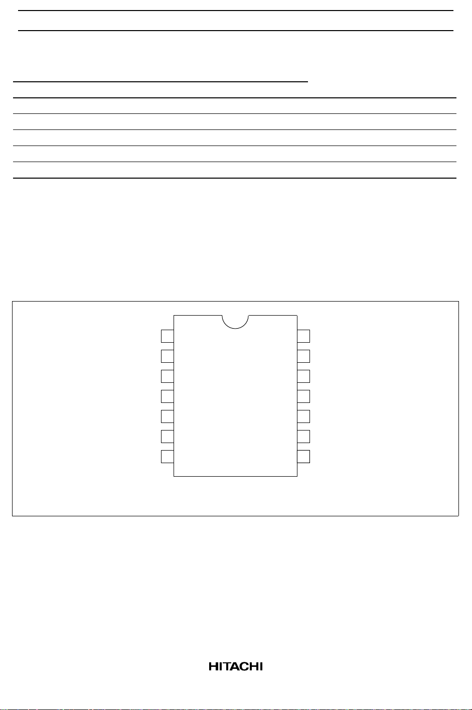
Pin Arrangement
1CLK
1CLR
1QA
1QB
1QC
1QD
GND
V
1
2
3
4
5
6
7
(Top view)
14
13
12
11
10
9
8
CC
2CLK
2CLR
2QA
2QB
2QC
2QD
2
HD74LV393A
Absolute Maximum Ratings
Item Symbol Ratings Unit Conditions
Supply voltage range V
Input voltage range*
Output voltage range*
1
1, 2
Input clamp current I
Output clamp current I
Continuous output current I
Continuous current through
V
or GND
CC
Maximum power dissipation
at Ta = 25°C (in still air)*
3
CC
V
I
V
O
IK
OK
O
or I
I
CC
GND
P
T
Storage temperature Tstg –65 to 150 °C
Notes: The absolute maximum ratings are values which must not individually be exceeded, and furthermore,
no two of which may be realized at the same time.
1. The input and output voltage ratings may be exceeded if the input and output clamp-current
ratings are observed.
2. This value is limited to 5.5 V maximum.
3. The maximum package power dissipation was calculated using a junction temperature of 150°C.
–0.5 to 7.0 V
–0.5 to 7.0 V
–0.5 to VCC + 0.5 V Output: H or L
–0.5 to 7.0 VCC: OFF
–20 mA VI < 0
±50 mA VO < 0 or VO > V
±25 mA VO = 0 to V
CC
±70 mA
785 mW SOP
500 TSSOP
CC
3
HD74LV393A
Recommended Operating Conditions
Item Symbol Min Max Unit Conditions
Supply voltage range V
Input voltage range V
Output voltage range V
Output current I
CC
I
O
OH
I
OL
Input transition rise or fall rate ∆t /∆v 0 200 ns/V VCC = 2.3 to 2.7 V
Operating free-air temperature Ta –40 85 °C
Note: Unused or floating inputs must be held high or low.
2.0 5.5 V
0 5.5 V
0VCCV H or L
— –50 µAV
—–2 mAV
—–6 V
= 2.0 V
CC
= 2.3 to 2.7 V
CC
= 3.0 to 3.6 V
CC
— –12 VCC = 4.5 to 5.5 V
—50 µAV
= 2.0 V
CC
— 2 mA VCC = 2.3 to 2.7 V
—6 V
—12 V
= 3.0 to 3.6 V
CC
= 4.5 to 5.5 V
CC
0 100 VCC = 3.0 to 3.6 V
020 V
= 4.5 to 5.5 V
CC
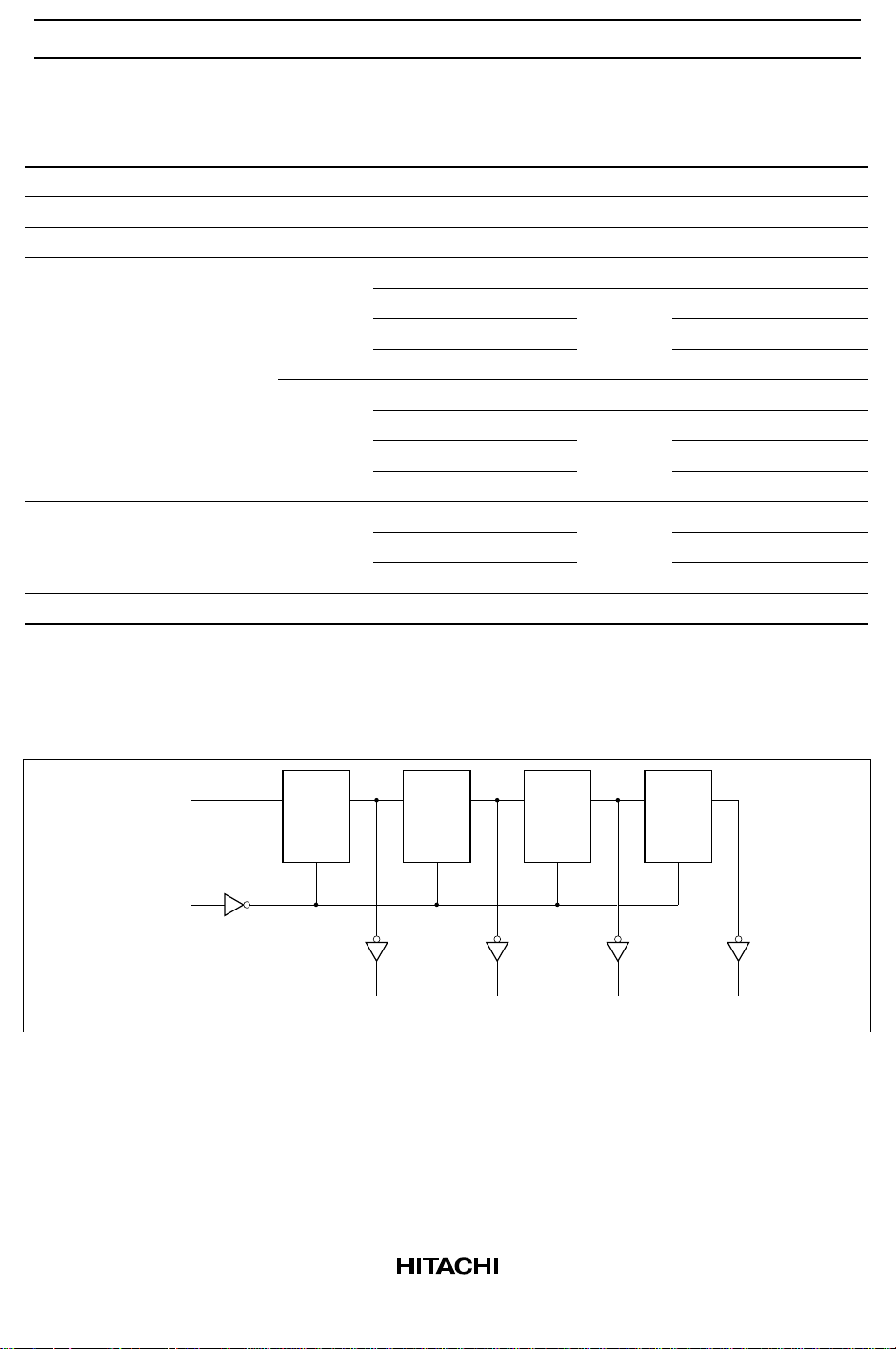
Logic Diagram
CLK
CLR
CK
QA
CK
Q
R
Q
R
QB
CK
QC
CK
Q
R
QD
Q
R
4
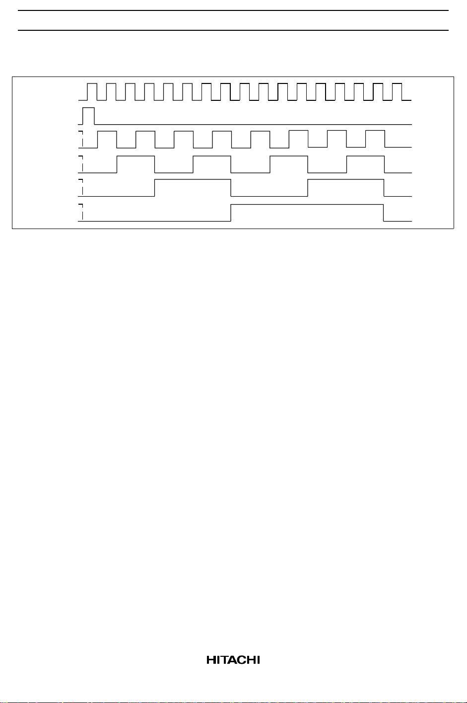
Timing Diagram
CLK
CLR
QA
QB
QC
QD
HD74LV393A
5
 Loading...