

HIT HD74LV166A Datasheet
HD74LV166A
Parallel-Load 8-bit Shift Register
ADE-205-268 (Z)
1st Edition
March 1999
Description
The HD74LV166A is 8-bit shift register with an output from the last stage. Data may be loaded into the
register either in parallel or in serial form. When the Shift/Load input is low, the data is loaded
asynchronously in parallel. When the Shift/Load input is high, the data is loaded serially on the rising edge
of either clock inhibit or Clock. Clear is asynchronous and active-low.
The 2-input NOR clock may be used either by combining two independent clock sources or by designating
one of the clock inputs to act as a clock inhibit.
Low-voltage and high-speed operation is suitable for the battery-powered products (e.g., notebook
computers), and the low-power consumption extends the battery life.
Features
• VCC = 2.0 V to 5.5 V operation
• All inputs VIH (Max.) = 5.5 V (@VCC = 0 V to 5.5 V)
• All outputs VO (Max.) = 5.5 V (@VCC = 0 V)
• Typical VOL ground bounce < 0.8 V (@VCC = 3.3 V, Ta = 25°C)
• Typical VOH undershoot > 2.3 V (@VCC = 3.3 V, Ta = 25°C)
• Output current ±6 mA (@VCC = 3.0 V to 3.6 V), ±12 mA (@VCC = 4.5 V to 5.5 V)
HD74LV166A
Function Table
Inputs Internal outputs Output
CLR SH/LD CLK INH CLK SER A ... H QA QB QH
LXXXXXLL L
HXLLXXQA0Q
B0
HLL ↑ X a ... h a b h
HHL ↑ HXHQAnQ
HHL ↑ LXLQAnQ
HXH↑ XXQA0Q
B0
Note: H: High level
L: Low level
↑: Low to high transition
X: Immaterial
a ... h: Parallel data
... QH0: Outputs remain unchanged.
Q
A0
Q
... QGn: Data shifted from the previous stage on a positive edge at the clock input.
An
Q
H0
Gn
Gn
Q
H0
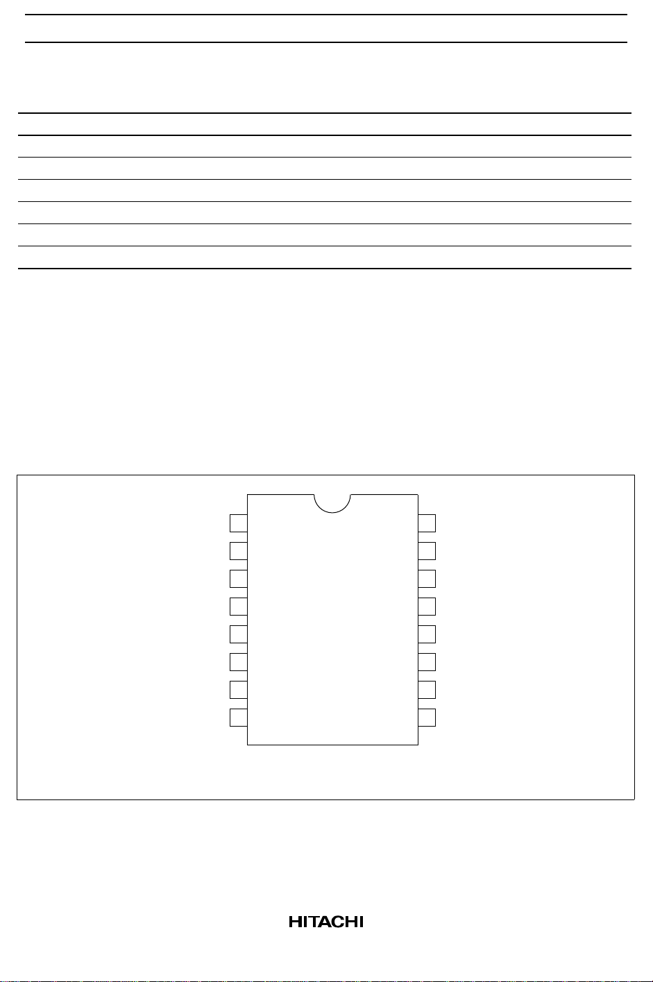
Pin Arrangement
SER
CLK INH
CLK
GND
V
1
2
A
3
B
4
C
5
D
6
7
8
16
15
14
13
12
11
10
9
CC
SH/LD
H
QH
G
F
E
CLR
(Top view)
2
HD74LV166A
Absolute Maximum Ratings
Item Symbol Ratings Unit Conditions
Supply voltage range V
Input voltage range*
Output voltage range*
1
1, 2
Input clamp current I
Output clamp current I
Continuous output current I
Continuous current through
V
or GND
CC
Maximum power dissipation
at Ta = 25°C (in still air)*
3
CC
V
I
V
O
IK
OK
O
or I
I
CC
GND
P
T
Storage temperature Tstg –65 to 150 °C
Notes: The absolute maximum ratings are values which must not individually be exceeded, and furthermore,
no two of which may be realized at the same time.
1. The input and output voltage ratings may be exceeded if the input and output clamp-current
ratings are observed.
2. This value is limited to 5.5 V maximum.
3. The maximum package power dissipation was calculated using a junction temperature of 150°C.
–0.5 to 7.0 V
–0.5 to 7.0 V
–0.5 to VCC + 0.5 V Output: H or L
–0.5 to 7.0 VCC: OFF
–20 mA VI < 0
±50 mA VO < 0 or VO > V
±25 mA VO = 0 to V
CC
±50 mA
785 mW SOP
500 TSSOP
CC
3
HD74LV166A
Recommended Operating Conditions
Item Symbol Min Max Unit Conditions
Supply voltage range V
Input voltage range V
Output voltage range V
Output current I
CC
I
O
OH
I
OL
Input transition rise or fall rate ∆t /∆v 0 200 ns/V VCC = 2.3 to 2.7 V
Operating free-air temperature Ta –40 85 °C
Note: Unused or floating inputs must be held high or low.
2.0 5.5 V
0 5.5 V
0VCCV H or L
— –50 µAV
—–2 mAV
—–6 V
= 2.0 V
CC
= 2.3 to 2.7 V
CC
= 3.0 to 3.6 V
CC
— –12 VCC = 4.5 to 5.5 V
—50 µAV
= 2.0 V
CC
— 2 mA VCC = 2.3 to 2.7 V
—6 V
—12 V
= 3.0 to 3.6 V
CC
= 4.5 to 5.5 V
CC
0 100 VCC = 3.0 to 3.6 V
020 V
= 4.5 to 5.5 V
CC
4
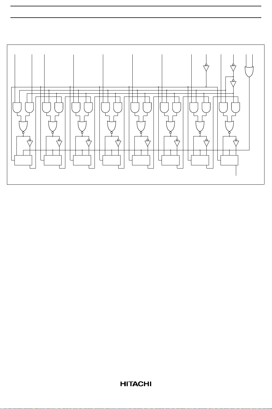
Logic Diagram
HD74LV166A
ACBDEFCLR SH/LDGH
SER
RCPS
CDQ
RCPS
D
C
CLK CLK INH
Q
QH
5
 Loading...