

HIT HD74LV164A Datasheet

HD74LV164A
8-bit Parallel-out Serial-in Shift Register
ADE-205-266 (Z)
1st Edition
March 1999
Description
The HD74LV164A is 8-bit shift register has gated serial inputs and clear. Each register bit is a D-type
master/slave flip-flop. Inputs A & B permit complete control over the incoming data. A low at either or
both inputs inhibits entry of new data and resets the first flip-flop to the low level at the next clock pulse. A
high level on one input enables the other input which will then determine the state of the first flip-flop.
Data at the serial inputs may be changed while the clock is high or low, but only information meeting the
setup and hold time but only information meeting the setup and hold time requirements will be entered.
Data is serially shifted in and out of the 8-bit register during the positive going transition of the clock pulse.
Clear is independent of the clock and accomplished by low level at the clear input.
Low-voltage and high-speed operation is suitable for the battery-powered products (e.g., notebook
computers), and the low-power consumption extends the battery life.
Features
• VCC = 2.0 V to 5.5 V operation
• All inputs VIH (Max.) = 5.5 V (@VCC = 0 V to 5.5 V)
• All outputs VO (Max.) = 5.5 V (@VCC = 0 V)
• Typical VOL ground bounce < 0.8 V (@VCC = 3.3 V, Ta = 25°C)
• Typical VOH undershoot > 2.3 V (@VCC = 3.3 V, Ta = 25°C)
• Output current ±6 mA (@VCC = 3.0 V to 3.6 V), ±12 mA (@VCC = 4.5 V to 5.5 V)
HD74LV164A
2
Function Table
Inputs Outputs
CLR CLK A B QA QB ... QD
L X X X L L ... L
H ↓ XXQA0Q
B0
... Q
H0
H ↑ HHHQAn... Q
Gn
H ↑ LXLQAn... Q
Gn
H ↑ XLLQAn... Q
Gn
Note: H: High level
L: Low level
X: Immaterial
↑: Low to high transition
↓: High to low transition
Q
AD
, QB0...QH0: Outputs remain unchanged.
Q
An
, QBn...QGn: Data shifted from the previous stage on a positive edge at the clock input.
Pin Arrangement
11
12
9
10
13
14
8
V
CC
Q
H
Q
G
Q
F
Q
E
CLR
1
2
3
4
5
6
7
A
B
Q
A
Q
B
Q
C
Q
D
GND
CLK
(Top view)
HD74LV164A
3
Absolute Maximum Ratings
Item Symbol Ratings Unit Conditions
Supply voltage range V
CC
–0.5 to 7.0 V
Input voltage range*
1
V
I
–0.5 to 7.0 V
Output voltage range*
1, 2
V
O
–0.5 to VCC + 0.5 V Output: H or L
–0.5 to 7.0 VCC: OFF
Input clamp current I
IK
–20 mA VI < 0
Output clamp current I
OK
±50 mA VO < 0 or VO > V
CC
Continuous output current I
O
±25 mA VO = 0 to V
CC
Continuous current through
V
CC
or GND
I
CC
or I
GND
±50 mA
Maximum power dissipation
at Ta = 25°C (in still air)*
3
P
T
785 mW SOP
500 TSSOP
Storage temperature Tstg –65 to 150 °C
Notes: The absolute maximum ratings are values which must not individually be exceeded, and furthermore,
no two of which may be realized at the same time.
1. The input and output voltage ratings may be exceeded if the input and output clamp-current
ratings are observed.
2. This value is limited to 5.5 V maximum.
3. The maximum package power dissipation was calculated using a junction temperature of 150°C.
HD74LV164A
4
Recommended Operating Conditions
Item Symbol Min Max Unit Conditions
Supply voltage range V
CC
2.0 5.5 V
Input voltage range V
I
0 5.5 V
Output voltage range V
O
0VCCV H or L
Output current I
OH
— –50 µAV
CC
= 2.0 V
—–2 mAV
CC
= 2.3 to 2.7 V
—–6 V
CC
= 3.0 to 3.6 V
— –12 VCC = 4.5 to 5.5 V
I
OL
—50 µAV
CC
= 2.0 V
— 2 mA VCC = 2.3 to 2.7 V
—6 V
CC
= 3.0 to 3.6 V
—12 V
CC
= 4.5 to 5.5 V
Input transition rise or fall rate ∆t /∆v 0 200 ns/V VCC = 2.3 to 2.7 V
0 100 VCC = 3.0 to 3.6 V
020 V
CC
= 4.5 to 5.5 V
Operating free-air temperature Ta –40 85 °C
Note: Unused or floating inputs must be held high or low.
HD74LV164A
5
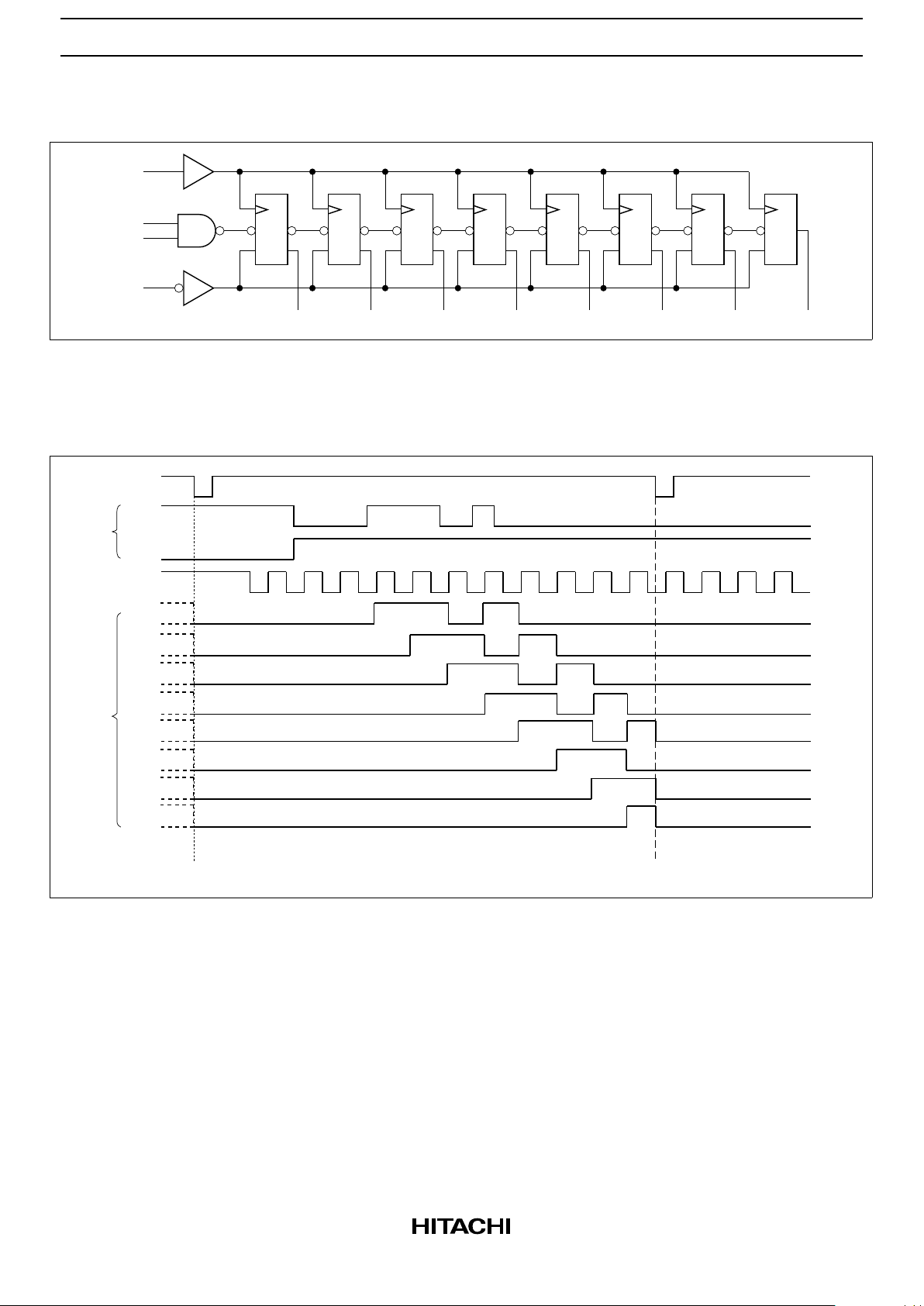
Logic Diagram
CLK
A
B
CLR
C1
1D
R
Q
A
3
C1
1D
R
Q
B
4
C1
1D
R
Q
C
5
C1
1D
R
Q
D
6
C1
1D
R
Q
E
10
C1
1D
R
Q
F
11
C1
1D
R
Q
G
12
C1
1D
R
Q
H
13
8
1
2
9
Timing Diagram
CLR
Clear Clear
CLK
Q
A
Q
B
Q
C
Q
D
Q
E
Q
F
Q
G
Q
H
A
B
 Loading...