

HIT HD74LV139A Datasheet
HD74LV139A
Dual 2-to-4 line Decoder / Demultiplexers
ADE-205-262 (Z)
1st Edition
March 1999
Description
The HD74LV139A is designed to be used in high-performance memory-decoding or data-routing
applications requiring very short propagation delay times. The active-low enable input can be used as a
data line in demultiplexing applications.
This decoder/demultiplexer features fully buffered inputs, each of which represents only one normalized
load to its driving circuit.
Low-voltage and high-speed operation is suitable for the battery-powered products (e.g., notebook
computers), and the low-power consumption extends the battery life.
Features
• VCC = 2.0 V to 5.5 V operation
• All inputs VIH (Max.) = 5.5 V (@VCC = 0 V to 5.5 V)
• All outputs VO (Max.) = 5.5 V (@VCC = 0 V)
• Typical VOL ground bounce < 0.8 V (@VCC = 3.3 V, Ta = 25°C)
• Typical VOH undershoot > 2.3 V (@VCC = 3.3 V, Ta = 25°C)
• Output current ±6 mA (@VCC = 3.0 V to 3.6 V), ±12 mA (@VCC = 4.5 V to 5.5 V)
Function Table
Inputs
Select Outputs
G1B A Y0Y1Y2Y3
HXXHHHH
LLLLHHH
LL HHL HH
LHLHHLH
LHHHHHL
Note: H: High level
L: Low level
X: Immaterial
HD74LV139A
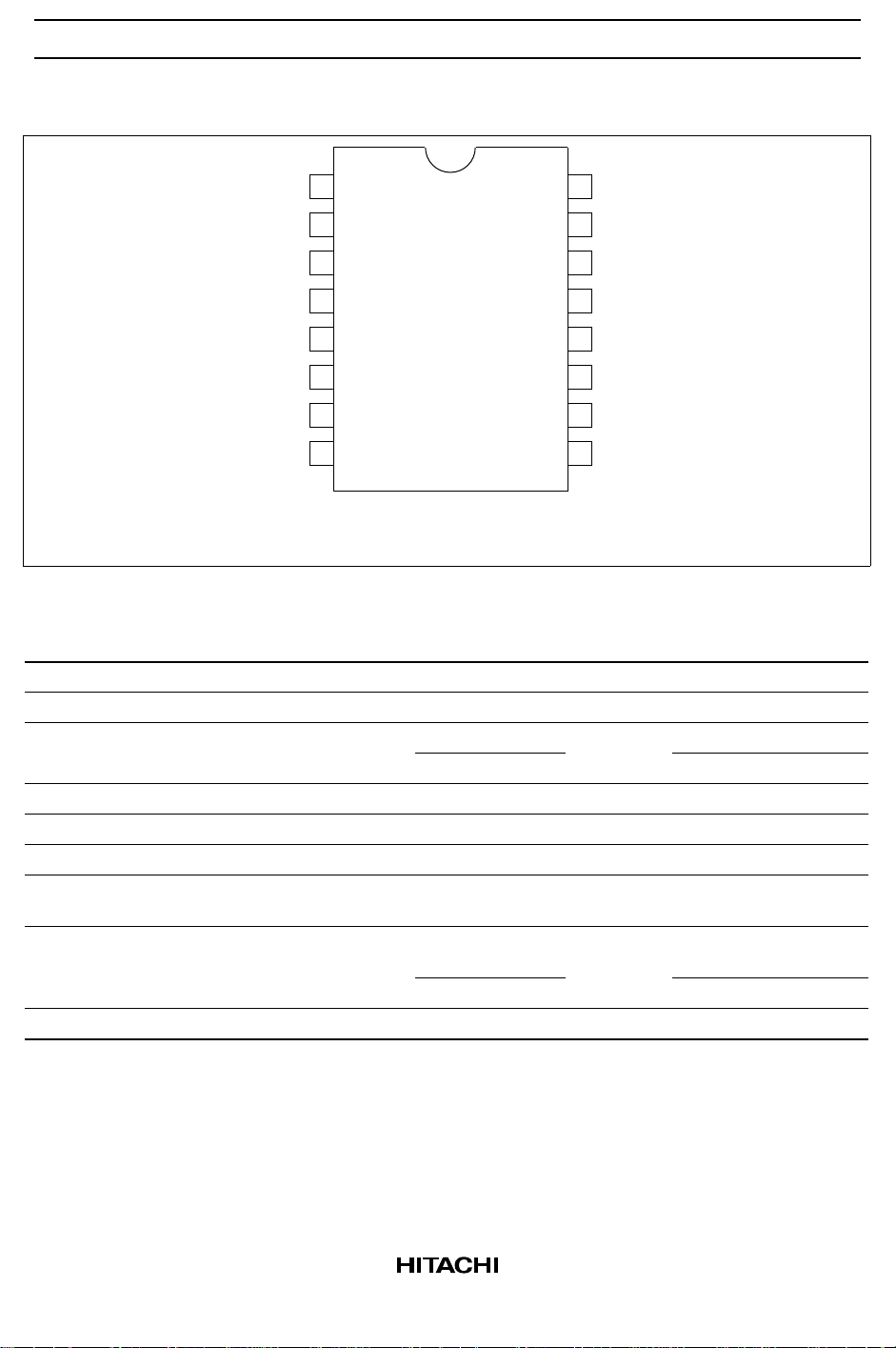
Pin Arrangement
1G
V
1
16
CC
1A
1B
1Y0
1Y1
1Y2
1Y3
GND
2
3
4
5
6
7
8
15
14
13
12
11
10
2G
2A
2B
2Y0
2Y1
2Y2
9
2Y3
(Top view)
Absolute Maximum Ratings
Item Symbol Ratings Unit Conditions
Supply voltage range V
Input voltage range*
Output voltage range*
1
1, 2
Input clamp current I
Output clamp current I
Continuous output current I
Continuous current through
V
or GND
CC
Maximum power dissipation
at Ta = 25°C (in still air)*
3
CC
V
I
V
O
IK
OK
O
or I
I
CC
GND
P
T
Storage temperature Tstg –65 to 150 °C
Notes: The absolute maximum ratings are values which must not individually be exceeded, and furthermore,
no two of which may be realized at the same time.
1. The input and output voltage ratings may be exceeded if the input and output clamp-current
ratings are observed.
2. This value is limited to 5.5 V maximum.
3. The maximum package power dissipation was calculated using a junction temperature of 150°C.
–0.5 to 7.0 V
–0.5 to 7.0 V
–0.5 to VCC + 0.5 V Output: H or L
–0.5 to 7.0 VCC: OFF
–20 mA VI < 0
±50 mA VO < 0 or VO > V
±25 mA VO = 0 to V
CC
±50 mA
785 mW SOP
500 TSSOP
CC
2
HD74LV139A
Recommended Operating Conditions
Item Symbol Min Max Unit Conditions
Supply voltage range V
Input voltage range V
Output voltage range V
Output current I
CC
I
O
OH
I
OL
Input transition rise or fall rate ∆t/∆v 0 200 ns/V VCC = 2.3 to 2.7 V
Operating free-air temperature Ta –40 85 °C
Note: Unused or floating inputs must be held high or low.
2.0 5.5 V
0 5.5 V
0VCCV H or L
— –50 µAV
—–2 mAV
—–6 V
= 2.0 V
CC
= 2.3 to 2.7 V
CC
= 3.0 to 3.6 V
CC
— –12 VCC = 4.5 to 5.5 V
—50 µAV
= 2.0 V
CC
— 2 mA VCC = 2.3 to 2.7 V
—6 V
—12 V
= 3.0 to 3.6 V
CC
= 4.5 to 5.5 V
CC
0 100 VCC = 3.0 to 3.6 V
020 V
= 4.5 to 5.5 V
CC
3
HD74LV139A
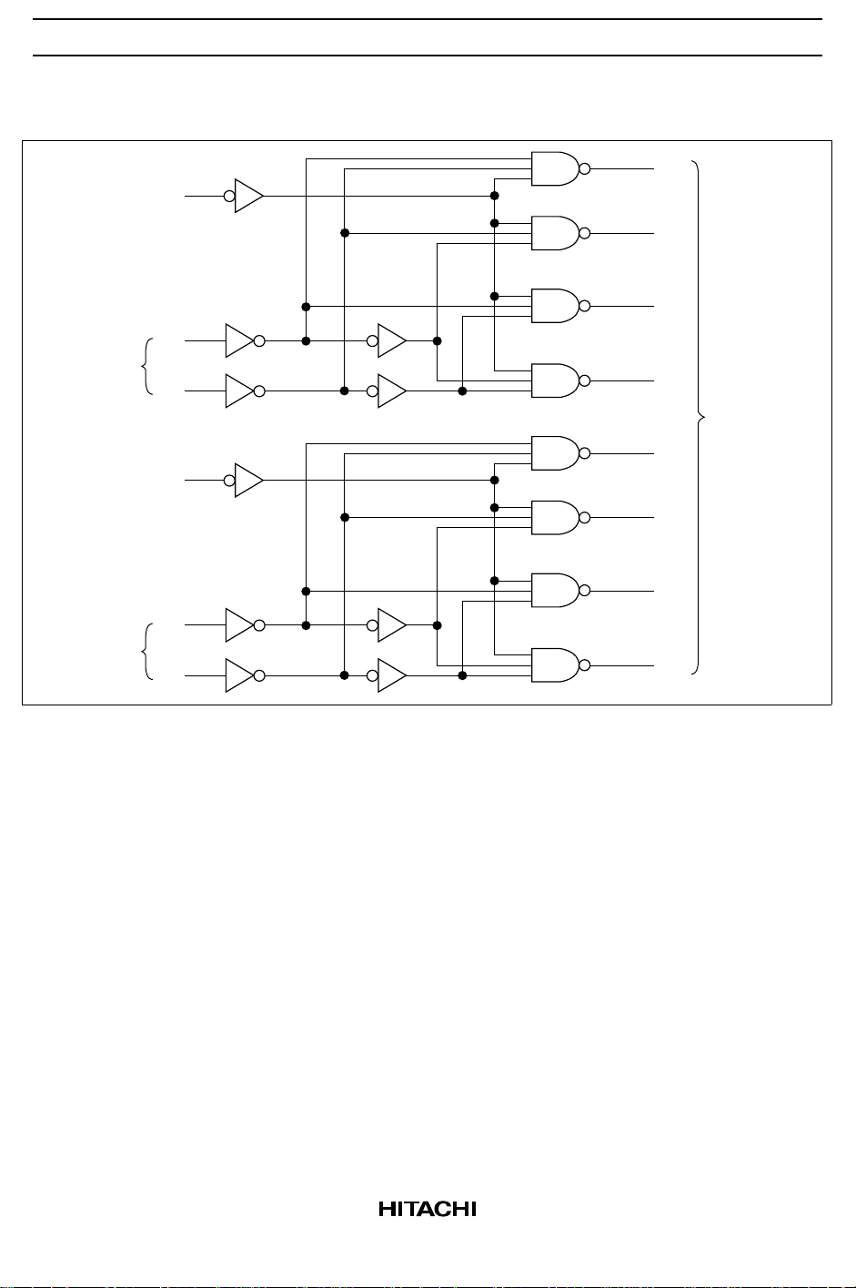
Logic Diagram
1G
Select
inputs
1A
1B
2G
4
1Y0
1
5
1Y1
6
1Y2
2
7
3
1Y3
Data
outputs
12
15
2Y0
11
2Y1
Select
inputs
2A
2B
10
2Y2
14
9
13
2Y3
4
 Loading...