

HIT HD74LV126A Datasheet
HD74LV126A
Quad. Bus Buffer Gates with 3-state Outputs
ADE-205-259 (Z)
1st Edition
March 1999
Description
The HD74LV126A features independent line drivers with three state outputs. Each output is disabled when
the associated output enable (OE) input is low. To ensure the high impedance state during power up or
power down, OE should be connected to GND through a pull-down resistor; the minimum value of the
resistor is determined by the current souring capability of the driver. Low-voltage and high-speed operation
is suitable for the battery-powered products (e.g., notebook computers), and the low-power consumption
extends the battery life.
Features
• VCC = 2.0 V to 5.5 V operation
• All inputs VIH (Max.) = 5.5 V (@VCC = 0 V to 5.5 V)
• All outputs VO (Max.) = 5.5 V (@VCC = 0 V)
• Typical VOL ground bounce < 0.8 V (@VCC = 3.3 V, Ta = 25°C)
• Typical VOH undershoot > 2.3 V (@VCC = 3.3 V, Ta = 25°C)
• Output current ±8 mA (@VCC = 3.0 V to 3.6 V), ±16 mA (@VCC = 4.5 V to 5.5 V)
Function Table
Inputs
OE A Output Y
HHH
HLL
LXZ
Note: H: High level
L: Low level
X: Immaterial
Z: High impedance
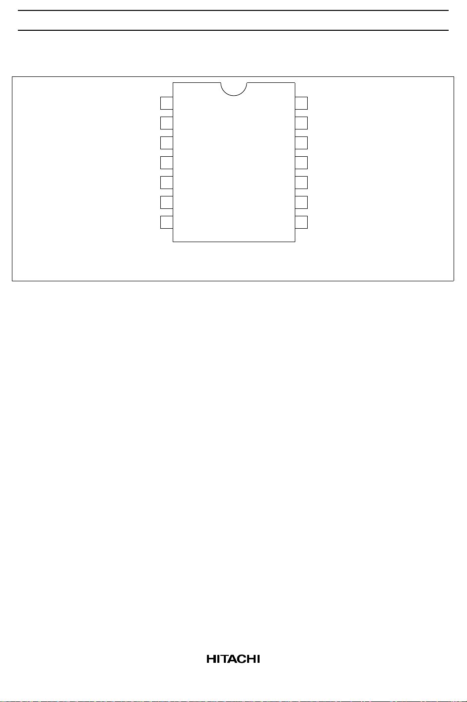
HD74LV126A
Pin Arrangement
1OE
V
1
14
CC
1A
1Y
2OE
2A
2Y
GND
2
3
4
5
6
7
(Top view)
13
12
11
10
4OE
4A
4Y
3OE
9
3A
8
3Y
2
HD74LV126A
Absolute Maximum Ratings
Item Symbol Ratings Unit Conditions
Supply voltage range V
Input voltage range*
Output voltage range*
1
1, 2
Input clamp current I
Output clamp current I
Continuous output current I
Continuous current through
V
or GND
CC
Maximum power dissipation
at Ta = 25°C (in still air)*
3
CC
V
I
V
O
IK
OK
O
or I
I
CC
GND
P
T
Storage temperature Tstg –65 to 150 °C
Notes: The absolute maximum ratings are values which must not individually be exceeded, and furthermore,
no two of which may be realized at the same time.
1. The input and output voltage ratings may be exceeded if the input and output clamp-current
ratings are observed.
2. This value is limited to 5.5 V maximum.
3. The maximum package power dissipation was calculated using a junction temperature of 150°C.
–0.5 to 7.0 V
–0.5 to 7.0 V
–0.5 to VCC + 0.5 V Output: H or L
–0.5 to 7.0 VCC: OFF or Output: Z
–20 mA VI < 0
±50 mA VO < 0 or VO > V
±35 mA VO = 0 to V
CC
CC
±70 mA
785 mW SOP
500 TSSOP
3
HD74LV126A
Recommended Operating Conditions
Item Symbol Min Max Unit Conditions
Supply voltage range V
Input voltage range V
Output voltage range V
Output current I
CC
I
O
OH
I
OL
Input transition rise or fall rate ∆t /∆v 0 200 ns/V VCC = 2.3 to 2.7 V
Operating free-air temperature Ta –40 85 °C
Note: Unused or floating inputs must be held high or low.
2.0 5.5 V
0 5.5 V
0VCCV H or L
0 5.5 High impedance state
— –50 µAV
—–2 mAV
—–8 V
= 2.0 V
CC
= 2.3 to 2.7 V
CC
= 3.0 to 3.6 V
CC
— –16 VCC = 4.5 to 5.5 V
—50 µAV
= 2.0 V
CC
— 2 mA VCC = 2.3 to 2.7 V
—8 V
—16 V
= 3.0 to 3.6 V
CC
= 4.5 to 5.5 V
CC
0 100 VCC = 3.0 to 3.6 V
020 V
= 4.5 to 5.5 V
CC
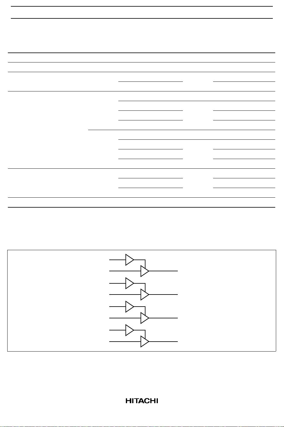
Logic Diagram
1OE
1A
2OE
2A
3OE
3A
4OE
1
2
4
5
10
9
13
12
3
1Y
6
2Y
8
3Y
11
4Y4A
4
HD74LV126A
DC Electrical Characteristics
• Ta = –40 to 85°C
Item Symbol VCC (V)* Min Typ Max Unit Test Conditions
Input voltage V
Output voltage V
Input current I
Off-state
IH
V
IL
OH
V
OL
IN
I
OZ
output current
Quiescent
I
CC
supply current
Output leakage
I
OFF
current
Input
C
IN
capacitance
Note: For conditions shown as Min or Max, use the appropriate values under recommended operating
conditions.
2.0 1.5 — — V
2.3 to 2.7 VCC × 0.7 — —
3.0 to 3.6 VCC × 0.7 — —
4.5 to 5.5 VCC × 0.7 — —
2.0 — — 0.5
2.3 to 2.7 — — VCC × 0.3
3.0 to 3.6 — — VCC × 0.3
4.5 to 5.5 — — VCC × 0.3
Min to
VCC – 0.1 — — V IOH = –50 µA
Max
2.3 2.0 — — IOH = –2 mA
3.0 2.48 — — IOH = –8 mA
4.5 3.8 — — IOH = –16 mA
Min to
— — 0.1 IOL = 50 µA
Max
2.3 — — 0.4 IOL = 2 mA
3.0 — — 0.44 IOL = 8 mA
4.5 — — 0.55 IOL = 16 mA
0 to 5.5 — — ±1 µAVI = 5.5 V or GND
5.5 — — ±5 µAVO = VCC or GND
5.5 — — 20 µAVI = VCC or GND, IO = 0
0——5 µAVI or VO = 0 V to 5.5 V
3.3 — 3 — pF VI = VCC or GND
5
 Loading...