HIT HD74HCT643, HD74HCT640 Datasheet

HD74HCT640/HD74HCT643
Octal Bus Transceivers (with 3-state outputs)
Description
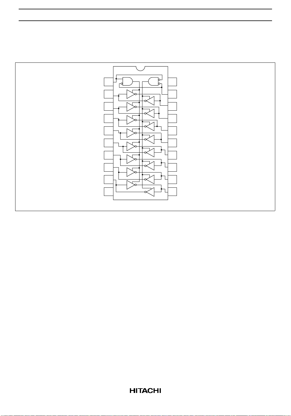
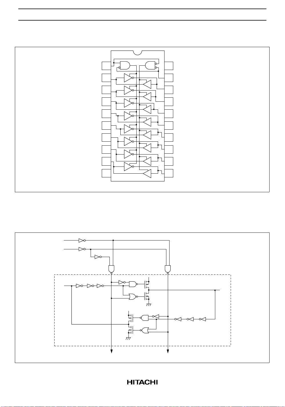
Both the HD74HCT640 and the HD74HCT643 have one active low enable input (G), and a direction
control (DIR). When the DIR input is high, data flows from the A inputs to the B outputs. When DIR is
low, data flows from B to A.
The HD74HCT640 transfers inverted data from one bus to the other. The HD74HCT643 transfers inverted
data from the A bus to the B bus and non-inverted data from the B bus to the A bus.
Features
• LSTTL Output Logic Level Compatibility as well as CMOS Output Compatibility
• High Speed Operation: tpd (A to B) = 14.5 ns typ (CL = 50 pF)
• High Output Current: Fanout of 15 LSTTL Loads
• Wide Operating Voltage: VCC = 4.5 to 5.5 V
• Low Input Current: 1 µA max
• Low Quiescent Supply Current: ICC (static) = 4 µA max (Ta = 25°C)
Function Table
Control Input Operation
G DIR HD74HCT640 HD74HCT643
LL B data to A bus B data to A bus
LH A data to B bus A data to B bus
H X Isolation Isolation

HD74HCT640/HD74HCT643
G
Pin Arrangement
HD74HCT640
DIR
1
A
2
1
20
19
V
CC
Enable
A2
A3
A4
A5
A6
A7
A8
GND
10
3
4
5
6
7
8
9
(Top view)
18
17
16
15
14
13
12
11
B1
B2
B3
B4
B5
B6
B7
B8
2

HD74HCT643
G
DIR
A
HD74HCT640/HD74HCT643
1
2
1
20
19
V
CC
Enable
Block Diagram
HD74HCT640
G
DIR
A2
A3
A4
A5
A6
A7
A8
GND
10
3
4
5
6
7
8
9
(Top view)
18
17
16
15
14
13
12
11
B1
B2
B3
B4
B5
B6
B7
B8
V
CC
A
V
CC
To 7 other inverters To 7 other inverters
B
3
 Loading...