HIT HD74HCT623, HD74HCT620 Datasheet

HD74HCT620/HD74HCT623
Octal Bus Transceivers (with inverted 3-state outputs)/
Octal Bus Transceivers (with 3-state outputs)
Description
This octal transceiver is designed for asynchronous two-way communication between data buses. The
control function implementation allows for maximum flexibility in timng.
This device allows data transmission from A bus to the B bus or from the B bus to the A bus depending
upon the logic levels at the enable inputs (GBA and GAB).
The enable inputs can be used to disable the device so that the buses are affectively isolated.
The dual-enable configuration gives these devices the capability to store data by simultaneous enabling of
GBA and GAB. Each output reinforces its input in this transceiver configuration. Thus, when both control
inputs are enabled and all other data sources to the two sets of bus lines are at high impedance, both sets of
bus lines (16 in all) will remain at their last states. The 8-bit codes appearing on the two sets of buses will
be identical for the HD74HCT623 or complementary for the HD74HCT620.
Features
• LSTTL Output Logic Level Compatibility as well as CMOS Output Compatibility
• High Speed Operation: tpd (Bus to Bus) = 15 ns typ (CL = 50 pF)
• High Output Current: Fanout of 15 LSTTL Loads
• Wide Operating Voltage: VCC = 4.5 to 5.5 V
• Low Input Current: 1 µA max
• Low Quiescent Supply Current: ICC (static) = 4 µA max (Ta = 25°C)

HD74HCT620/HD74HCT623
A
Function Table
Enable Input Operation
GBA GAB HD74HCT620 HD74HCT623
LL B data to A bus B data to A bus
HH A data to B bus A data to B bus
H L Isolation Isolation
LH B data to A bus,
A data to B bus
Pin Arrangement
B data to A bus,
A data to B bus
Enable GAB
A
A2
A3
A4
A5
A6
A7
A8
GND
1
2
1
3
4
5
6
7
8
9
10
(Top view)
V
20
19
Enable GB
18
B
17
B2
16
B3
15
B4
14
B5
13
B6
12
B7
11
B8
CC
1
2

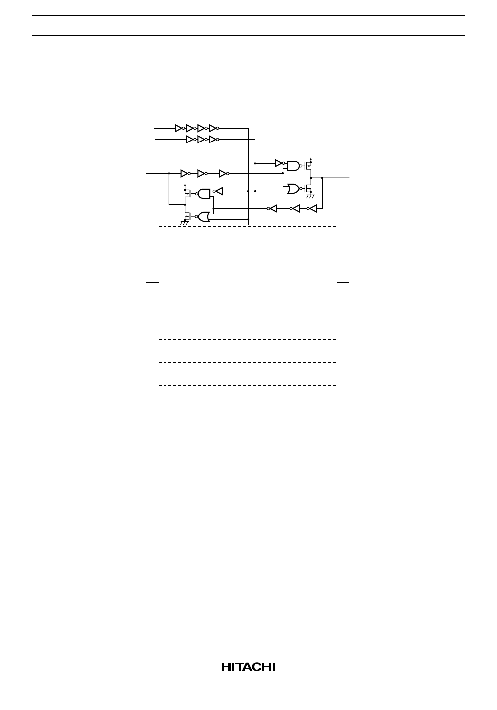
Block Diagram
HD74HCT620
GAB
GBA
HD74HCT620/HD74HCT623
V
CC
A1
V
CC
A2
A3
A4 B4
A5 B5
A6 B6
A7 B7
A8 B8
B2
B3
B
1
3
 Loading...