

HIT HD74HCT245 Datasheet

HD74HCT245
Octal Bus Transceivers (with 3-state outputs)
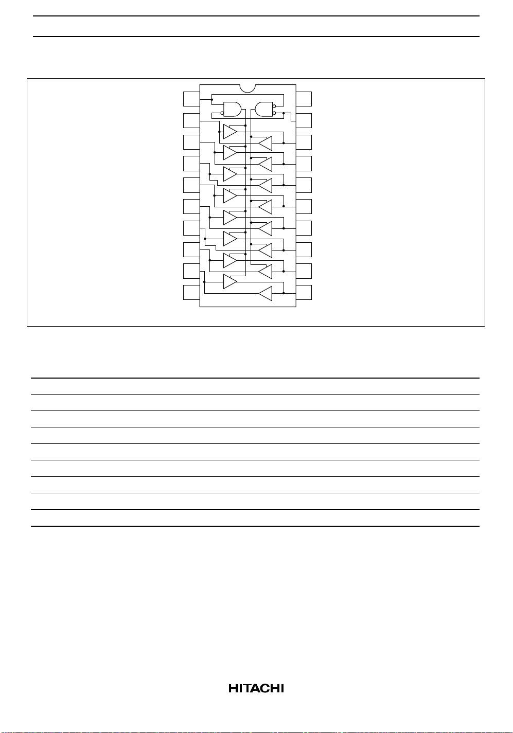
Description
This device has an active low enable input G and a direction control input (DIR). When DIR is high, data
flows from the A inputs to the B outputs. When DIR is low, data flows from the B inputs to the A outputs.
The HD74HCT245 transfers true data from one bus to the other.
This device does not have schmitt trigger inputs.
Features
• LSTTL Output Logic Level Compatibility as well as CMOS Output Compatibility
• High Speed Operation: tpd (A to Y) = 12 ns typ (CL = 50 pF)
• High Output Current: Fanout of 15 LSTTL Loads
• Wide Operating Voltage: VCC = 4.5 to 5.5 V
• Low Input Current: 1 µA max
• Low Quiescent Supply Current: ICC (static) = 4 µA max (Ta = 25°C)
Function Table
Enable G Direction Control DIR Operation
L L B data to A bus
L H A data to B bus
H X Isolation
H : High level
L : Low level
X : Irrelevant
HD74HCT245
Pin Arrangement
DIR
A
1
2
1
20
19
V
CC
Enable G
A2
A3
A4
A5
A6
A7
A8
GND
3
4
5
6
7
8
9
10
18
17
16
15
14
13
12
11
B
B2
B3
B4
B5
B6
B7
B8
1
(Top view)
Absolute Maximum Ratings
Item Symbol Rating Unit
Supply voltage range V
Input voltage V
Output voltage V
DC current drain per pin I
DC current drain per VCC, GND ICC, I
DC input diode current I
DC output diode current I
Power dissipation per package P
CC
IN
OUT
OUT
GND
IK
OK
T
Storage temperature Tstg –65 to +150 °C
–0.5 to +7.0 V
–0.5 to VCC + 0.5 V
–0.5 to VCC + 0.5 V
±35 mA
±75 mA
±20 mA
±20 mA
500 mW
2
HD74HCT245
DC Characteristics
Ta = –40 to
Ta = 25°C
Item Symbol Min Typ Max Min Max Unit V
Input voltage V
Output voltage V
IH
V
IL
OH
2.0 — — 2.0 — V 4.5 to
— — 0.8 — 0.8 V 4.5 to
4.4 — — 4.4 — V 4.5 Vin = VIH or VILIOH = –20 µA
4.18 — — 4.13 — 4.5 IOH = –6 mA
V
OL
— — 0.1 — 0.1 V 4.5 Vin = VIH or VILIOL = 20 µA
— — 0.26 — 0.33 4.5 IOL = 6 mA
Off-state output
I
OZ
——±0.5 — ±5.0 µA 5.5 Vin = VIH or VIL,
current
Input current Iin — — ±0.1 — ±1.0 µA 5.5 Vin = VCC or GND
Quiescent current I
CC
— — 4.0 — 40 µA 5.5 Vin = VCC or GND, Iout = 0 µA
+85°C Test Conditions
(V)
CC
5.5
5.5
Vout = V
or GND
CC
AC Characteristics (CL = 50 pF, Input tr = tf = 6 ns)
Ta = –40 to
Ta = 25°C
Item Symbol Min Typ Max Min Max Unit V
Propagation delay t
time t
Output enable t
time t
Output disable t
time t
Output rise/fall
time
PLH
PHL
ZL
ZH
LZ
HZ
t
TLH
t
THL
— 11 22 — 28 ns 4.5
— 13 22 — 28 4.5
— 17 30 — 38 ns 4.5
— 14 30 — 38 4.5
— 20 30 — 38 ns 4.5
— 22 30 — 38 4.5
— 4 12 — 15 ns 4.5
Input capacitance Cin — 5 10 — 10 pF —
+85°C Test Conditions
(V)
CC
3
 Loading...