

HIT HD74HCT240 Datasheet
HD74HCT240
Octal Buffers/Line Drivers/Line Receivers
(with inverted 3-state outputs)
Description
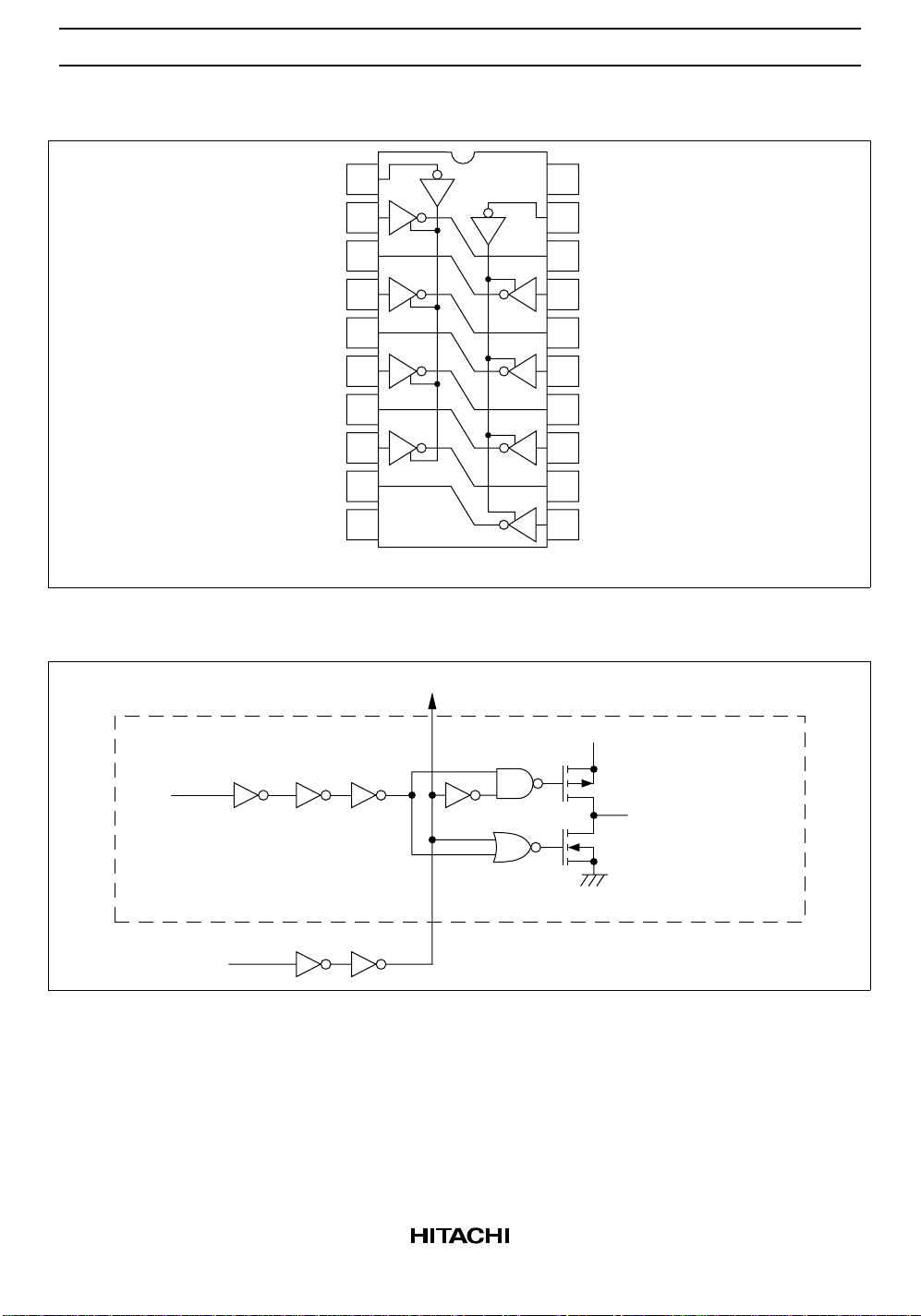
The HD74HCT240 is an inverting buffer and has two active low enables (1G and 2G). Each enable
independently controls 4 buffers. This device does not have schmitt trigger inputs.
Features
• LSTTL Output Logic Level Compatibility as well as CMOS Output Compatibility
• High Speed Operation: tpd (A to Y) = 11 ns typ (CL = 50 pF)
• High Output Current: Fanout of 15 LSTTL Loads
• Wide Operating Voltage: VCC = 4.5 to 5.5 V
• Low Input Current: 1 µA max
• Low Quiescent Supply Current: ICC (static) = 4 µA max (Ta = 25°C)
Function Table
Inputs Output
G AY
HX Z
LH L
LL H
H : High level
L : Low level
X : Irrelevant
Z : Off (high impedance) state of a 3-state output
HD74HCT240
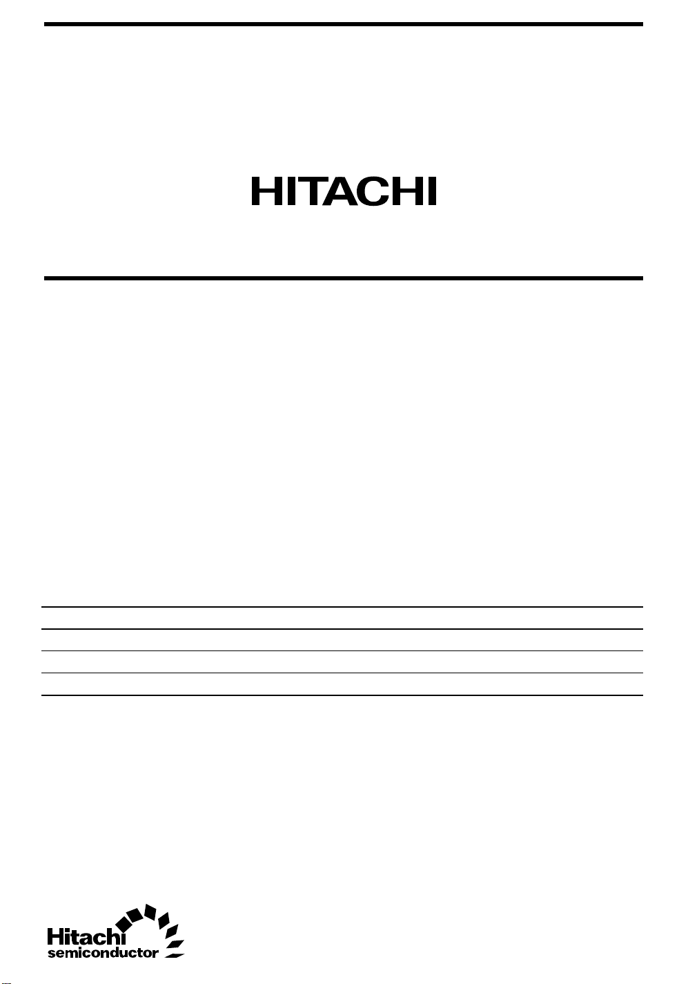
Pin Arrangement
1G
1A
1
2
1
20
19
V
2G
CC
Block Diagram
Input A
2Y
1A
2Y
1A
2Y
1A
2Y
GND
3
4
4
2
5
3
6
3
7
2
8
4
9
1
10
18
17
16
15
14
13
12
11
1Y
2A
1Y
2A
1Y
2A
1Y
2A
1
4
2
3
3
2
4
1
(Top view)
To three other
Inverters
V
CC
One of 8
Inverters
Y
Strobe G
2
HD74HCT240
Absolute Maximum Ratings
Item Symbol Rating Unit
Supply voltage range V
Input voltage V
Output voltage V
DC current drain per pin I
DC current drain per VCC, GND ICC, I
DC input diode current I
DC output diode current I
Power dissipation per package P
CC
IN
OUT
OUT
GND
IK
OK
T
Storage temperature Tstg –65 to +150 °C
DC Characteristics
Ta = –40 to
Ta = 25°C
Item Symbol Min Typ Max Min Max Unit V
Input voltage V
Output voltage V
IH
V
IL
OH
2.0 — — 2.0 — V 4.5 to
— — 0.8 — 0.8 V 4.5 to
4.4 — — 4.4 — V 4.5 Vin = VIH or VILIOH = –20 µA
4.18 — — 4.13 — 4.5 IOH = –6 mA
V
OL
— — 0.1 — 0.1 V 4.5 Vin = VIH or VILIOL = 20 µA
— — 0.26 — 0.33 4.5 IOL = 6 mA
Off-state output
I
OZ
——±0.5 — ±5.0 µA 5.5 Vin = VIH or VIL,
current
Input current Iin — — ±0.1 — ±1.0 µA 5.5 Vin = VCC or GND
Quiescent current I
CC
— — 4.0 — 40 µA 5.5 Vin = VCC or GND, Iout = 0 µA
+85°C Test Conditions
–0.5 to +7.0 V
–0.5 to VCC + 0.5 V
–0.5 to VCC + 0.5 V
±35 mA
±75 mA
±20 mA
±20 mA
500 mW
(V)
CC
5.5
5.5
Vout = V
or GND
CC
3
 Loading...