

HIT HD74HCT237 Datasheet

HD74HCT237
3-to-8-line Decoder/Demultiplexer with Address Latch
Description
The HD74HCT237 decodes a three-bit Address to one-of-eight active-high outputs. The device has a
transparent latch for storage of the Address. Two Chip Selects, one active-low and one active-high, are
provided to facilitate the demultiplexing, cascading, and chip-selecting functions.
The demultiplexing function is accomplished by using the Address inputs to select the desired device
output, and then by using one of the Chip Select as a data input while holding the other one active.
The HD74HCT237 is the noninverting version of the HD74HCT137.
Features
• LSTTL Output Logic Level Compatibility as well as CMOS Output Compatibility
• High Speed Operation: tpd (A, B, C to Y) = 23 ns typ (CL = 50 pF)
• High Output Current: Fanout of 10 LSTTL Loads
• Wide Operating Voltage: VCC = 4.5 to 5.5 V
• Low Input Current: 1 µA max
• Low Quiescent Supply Current: ICC (static) = 4 µA max (Ta = 25°C)
HD74HCT237
Function Table
Inputs
Enable Select Outputs
GL G
XXHXXXLLLLLLLL
XLXXXXLLLLLLLL
LHLLLLHLLLLLLL
LHLLLHLHLLLLLL
LHLLHLLLHLLLLL
LHLLHHLLLHLLLL
LHLHLLLLLLHLLL
LHLHLHLLLLLHLL
LHLHHLLLLLLLHL
LHLHHHLLLLLLLH
H H L X X X Output Corresponding to stored address L; all others H
G
1
CBAY0Y1Y2Y3Y4Y5Y6Y
2
7
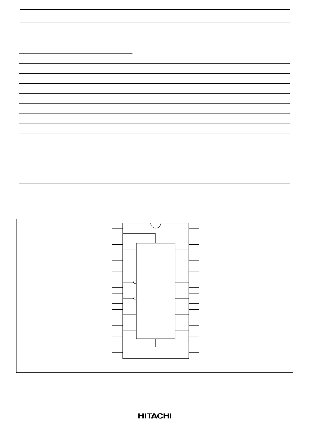
Pin Arrangement
A
GL
G
G
Y
GND
1
2
B
3
C
4
5
2
6
1
7
7
B
C
GL
G
G
Y
A
Y
0
Y
1
Y
2
2
1
7
Y
3
Y
4
Y
Y
5
6
8
16
15
14
13
12
11
10
V
CC
Y
0
Y
1
Y
2
Y
3
Y
4
Y
5
Y
9
6
(Top view)
2
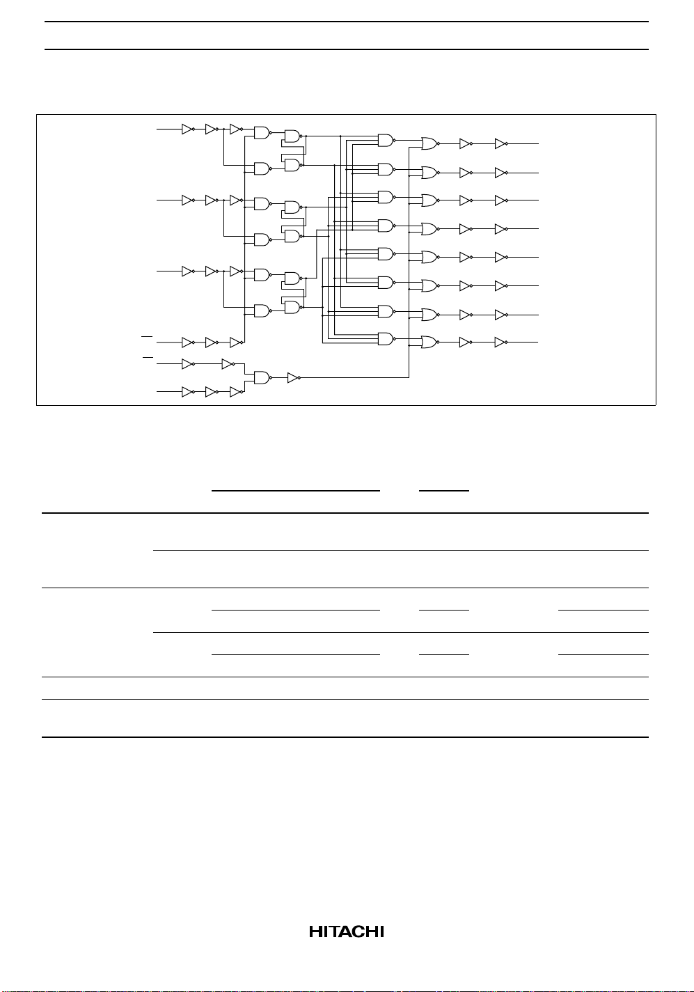
Logic Diagram
HD74HCT237
A
Y
0
Y
1
GL
G
G
B
C
2
1
Y
2
Y
3
Y
4
Y
5
Y
6
Y
7
DC Characteristics
Ta = –40 to
Ta = 25°C
Item Symbol Min Typ Max Min Max Unit V
Input voltage V
Output voltage V
IH
V
IL
OH
2.0 — — 2.0 — V 4.5 to
— — 0.8 — 0.8 V 4.5 to
4.4 — — 4.4 — V 4.5 Vin = VIH or VILIOH = –20 µA
4.18 — — 4.13 — 4.5 IOH = –4 mA
V
OL
— — 0.1 — 0.1 V 4.5 Vin = VIH or VILIOL = 20 µA
— — 0.26 — 0.33 4.5 IOL = 4 mA
Input current Iin — — ±0.1 — ±1.0 µA 5.5 Vin = VCC or GND
Quiescent supply
I
CC
— — 4.0 — 40 µA 5.5 Vin = VCC or GND, Iout = 0 µA
current
+85°C Test Conditions
(V)
CC
5.5
5.5
3
 Loading...