HIT HD74HC95 Datasheet

HD74HC95
4-bit Parallel Access Shift Register
Description
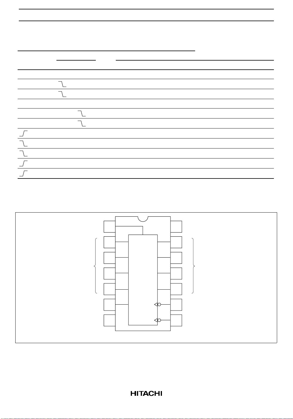
This 4-bit register features parallel and serial inputs, parallel outputs, mode control, and two clock inputs.
The register has three mode operation:
• Parallel (broadside) load
• Shift right (the direction QA toward QD)
• Shift left (the direction QD toward QA)
Parallel loading is accomplished by applying the four bits of data and taking the mode conrol input high.
The data is loaded into the associated flip-flops and appears at the outputs after the high-to-low transition of
the clock-2 input. During loading, the entry of serial data is inhibited. Shift right is accomplished on the
high-to-low transition of clock-1 when the mode control is low; shift left is accomplished on the high-tolow transition of clock-2 when the mode control is high by connecting the output of each flip-flop (QD to
input C, etc.) and serial data is entered at input D. The clock input may be applied commonly to clock-1
and clock-2 if both modes can be clocked from the same source. Changes at the mode control input should
normally be made while both clock inputs are low: however, conditions described in the last three lines of
the function table will also ensure that register contents are protected.
Features
• High Speed Operation: tpd (Clock to Q) = 17 ns typ (CL = 50 pF)
• High Output Current: Fanout of 10 LSTTL Loads
• Wide Operating Voltage: VCC = 2 to 6 V
• Low Input Current: 1 µA max
• Low Quiescent Supply Current: ICC (static) = 4 µA max (Ta = 25°C)

HD74HC95
Function Table
Inputs
Clocks Parallel Outputs
Mode Control 2 (L) 1 (R) Serial A B C D Q
H HXXXXXXQA0Q
H XXabcdabc d
H XXQB+Q
Q
C+
dQBnQ
D+
L LHXXXXXQA0Q
LXHXXXXHQAnQ
LXLXXXXLQAnQ
LLXXXXXQA0Q
LLXXXXXQA0Q
LHXXXXXQA0Q
HL XXXXXQA0Q
HHXXXXXQA0Q
Q
A
Q
B
Q
B0
Q
Cn
Q
B0
Q
B0
Q
B0
Q
B0
Q
B0
Q
B0
Q
C
C0
Dn
C0
Bn
Bn
C0
C0
C0
C0
C0
D
Q
D0
d
Q
D0
Q
Cn
Q
Cn
Q
D0
Q
D0
Q
D0
Q
D0
Q
D0
Pin Arrangement
Serial
Input
Inputs
Mode
Control
GND
1
Serial
Q
Input
A
QB
2
A
3
B
A
B
14
13
12
V
QA
QB
CC
Outputs
4
C
5
D
6
C
D
Mode
7
CK
CK
QC
QD
1
2
11
10
9
8
QC
QD
Clock1
R-Shift
Clock2
L-Shift
(Load)
(Top View)
2

HD74HC95
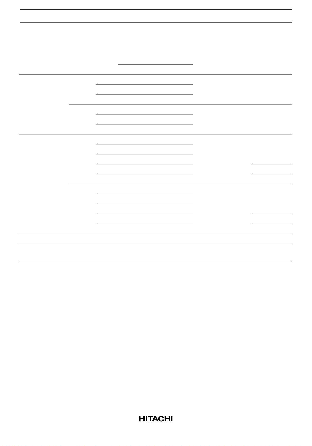
DC Characteristics
Ta = –40 to
Ta = 25°C
Item Symbol V
Input voltage V
IH
(V) Min Typ Max Min Max Unit Test Conditions
CC
2.0 1.5 — — 1.5 — V
4.5 3.15 — — 3.15 —
6.0 4.2 — — 4.2 —
V
IL
2.0 — — 0.5 — 0.5 V
4.5 — — 1.35 — 1.35
6.0 — — 1.8 — 1.8
Output voltage V
OH
2.0 1.9 2.0 — 1.9 — V Vin = VIH or VILIOH = –20 µA
4.5 4.4 4.5 — 4.4 —
6.0 5.9 6.0 — 5.9 —
4.5 4.18 — — 4.13 — IOH = –4 mA
6.0 5.68 — — 5.63 — IOH = –5.2 mA
V
OL
2.0 — 0.0 0.1 — 0.1 V Vin = VIH or VILIOL = 20 µA
4.5 — 0.0 0.1 — 0.1
6.0 — 0.0 0.1 — 0.1
4.5 — — 0.26 — 0.33 IOL = 4 mA
6.0 — — 0.26 — 0.33 IOL = 5.2 mA
Input current Iin 6.0 — — ±0.1 — ±1.0 µA Vin = VCC or GND
Quiescent supply
I
CC
6.0 — — 4.0 — 40 µA Vin = VCC or GND, Iout = 0 µA
current
+85°C
3
 Loading...