

HIT HD74HC77 Datasheet
HD74HC77
4-bit Bistable Latch
Description
The HD74HC77 is ideally suited for use as temporary storage for binary information between processing
units and input/output or indicator units. Information present at a data (D) input is transferred to the Q
output when the enable (G) is high and the Q output will follow the data input as long as the enable remains
high. When the enable goes low the information (that was present at the data input at the time the transition
occurred) is retained at the Q output until the enable is permitted to go high.
Features
• High Speed Operation: tpd (D to Q) = 12 ns typ (CL = 50 pF)
• High Output Current: Fanout of 10 LSTTL Loads
• Wide Operating Voltage: VCC = 2 to 6 V
• Low Input Current: 1 µA max
• Low Quiescent Supply Current: ICC (static) = 2 µA max (Ta = 25°C)
Function Table
Inputs Output
DG Q
LH L
HH H
X L No change
HD74HC77
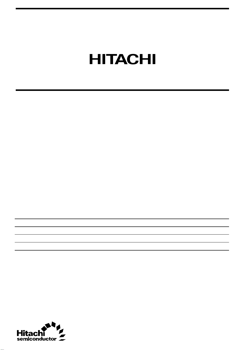
Pin Arrangement
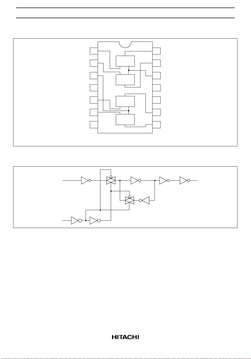
Block Diagram (1//4)
Data Q
1D
2D
Enable3-4
V
CC
3D
4D
NC
14
1
2
3
4
5
6
7
Q
DG
DG
Q
Q
DG
DG
Q
(Top view)
1Q
13
2Q
12
Enable1-2
11
GND
10
NC
9
3Q
8
4Q
Enable
2
HD74HC77
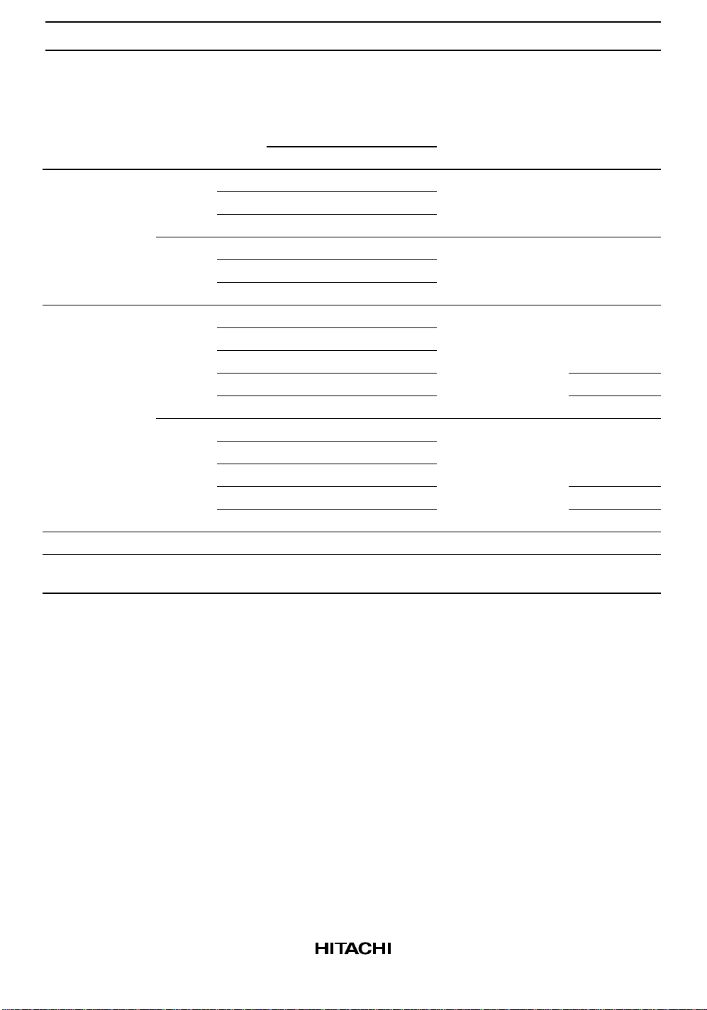
DC Characteristics
Ta = –40 to
Ta = 25°C
Item Symbol V
Input voltage V
IH
(V) Min Typ Max Min Max Unit Test Conditions
CC
2.0 1.5 — — 1.5 — V
4.5 3.15 — — 3.15 —
6.0 4.2 — — 4.2 —
V
IL
2.0 — — 0.5 — 0.5 V
4.5 — — 1.35 — 1.35
6.0 — — 1.8 — 1.8
Output voltage V
OH
2.0 1.9 2.0 — 1.9 — V Vin = VIH or VILIOH = –20 µA
4.5 4.4 4.5 — 4.4 —
6.0 5.9 6.0 — 5.9 —
4.5 4.18 — — 4.13 — IOH = –4 mA
6.0 5.68 — — 5.63 — IOH = –5.2 mA
V
OL
2.0 — 0.0 0.1 — 0.1 V Vin = VIH or VILIOL = 20 µA
4.5 — 0.0 0.1 — 0.1
6.0 — 0.0 0.1 — 0.1
4.5 — — 0.26 — 0.33 IOL = 4 mA
6.0 — — 0.26 — 0.33 IOL = 5.2 mA
Input current Iin 6.0 — — ±0.1 — ±1.0 µA Vin = VCC or GND
Quiescent supply
I
CC
6.0 — — 2.0 — 20 µA Vin = VCC or GND, Iout = 0 µA
current
+85°C
3
 Loading...