

HIT HD74HC74 Datasheet
HD74HC74
Dual D-type Flip-Flops (with Preset and Clear)
Description
The flip-flop has independent data, preset, clear, and clock inputs and Q and Q outputs. The logic level
present at thte data input is transferred to the output during the positive going transition to the clock pulse.
Preset and clear are independent of the clock and accomplished by a low level at the appropriate input.
Features
• High Speed Operation: tpd (Clock to Q or Q) = 14 ns typ (CL = 50 pF)
• High Output Current: Fanout of 10 LSTTL Loads
• Wide Operating Voltage: VCC = 2 to 6 V
• Low Input Current: 1 µA max
• Low Quiescent Supply Current: ICC (static) = 2 µA max (Ta = 25°C)
Function Table
Inputs Outputs
Preset Clear Clock Data Q Q
LH X X H L
HL X X L H
LL X X H*
HH HHL
HH LLH
H H L X no change no change
H H H X no change no change
HH X no change no change
Note: 1. Q and Q will remain HIGH as long as Preset and Clear are Low, but Q and Q are unpredictable,
if Preset and Clear go HIGH simultaneously.
1
H*
1
HD74HC74
(
)
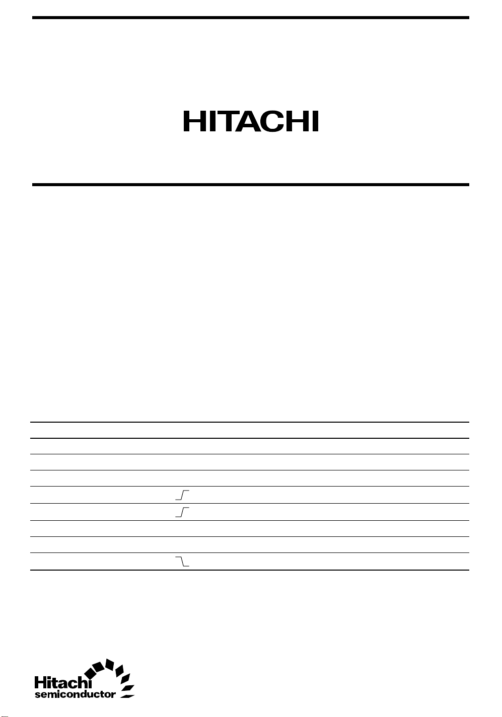
Pin Arrangement
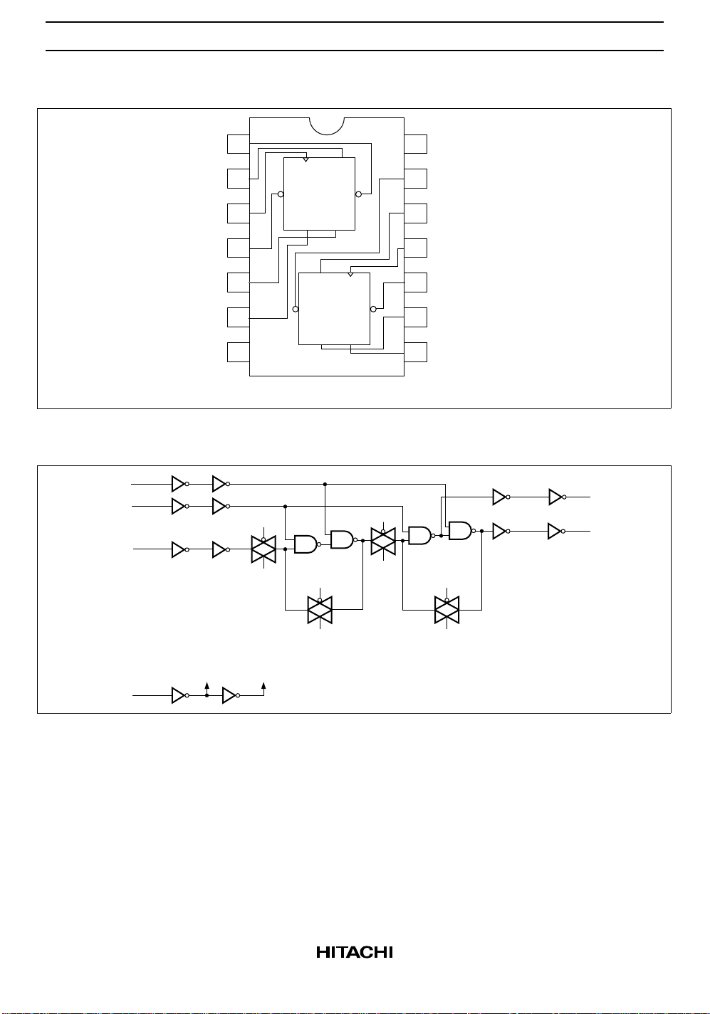
Logic Diagram (1/2)
PR
CLR
D
1CLR
1D
1CK
1PR
1Q
1Q
GND
V
CK
CK
14
13
12
11
10
9
8
CC
2CLR
2D
2CK
2PR
2Q
2Q
Q
Q
CK
1
2
3
4
5
6
7
CK
#
CK
CK D
PR CLR
Q Q
DCK
CLR PR
Q Q
Top view
#
CK
#
CK
#
CK
2
CK
CK
#
CK
HD74HC74
DC Characteristics
Ta = –40 to
Ta = 25°C
Item Symbol V
Input voltage V
IH
(V) Min Typ Max Min Max Unit Test Conditions
CC
2.0 1.5 — — 1.5 — V
4.5 3.15 — — 3.15 —
6.0 4.2 — — 4.2 —
V
IL
2.0 — — 0.5 — 0.5 V
4.5 — — 1.35 — 1.35
6.0 — — 1.8 — 1.8
Output voltage V
OH
2.0 1.9 2.0 — 1.9 — V Vin = VIH or VILIOH = –20 µA
4.5 4.4 4.5 — 4.4 —
6.0 5.9 6.0 — 5.9 —
4.5 4.18 — — 4.13 — IOH = –4 mA
6.0 5.68 — — 5.63 — IOH = –5.2 mA
V
OL
2.0 — 0.0 0.1 — 0.1 V Vin = VIH or VILIOL = 20 µA
4.5 — 0.0 0.1 — 0.1
6.0 — 0.0 0.1 — 0.1
4.5 — — 0.26 — 0.33 IOL = 4 mA
6.0 — — 0.26 — 0.33 IOL = 5.2 mA
Input current Iin 6.0 — — ±0.1 — ±1.0 µA Vin = VCC or GND
Quiescent supply
I
CC
6.0 — — 2.0 — 20 µA Vin = VCC or GND, Iout = 0 µA
current
+85°C
3
 Loading...