

HIT HD74HC680 Datasheet

HD74HC680
12-bit Address Comparator
Description
The HD74HC680 address comparator simplifies addressing of memory boards and/or other peripheral
devices. The four P inputs are normally hard wired with a preprogrammed address. An internal decoder
determines what input information applied to the 12 A inputs must be low or high to cause a low state at the
output (Y). For example, a positive-logic bit combination of 0111 (decimal 7) at the P input determines
that inputs A1 through A7 must be low and that inputs A8 through A12 must be high to cause the output to go
low. Equality of the address applied at the A inputs to the preprogrammed address is indicated by the
output being low.
The HD74HC680 features a transparent latch and a latch enable input (C). When C is high, the device is in
the transparent mode. When C is low, the previous logical state of Y is latched.
Features
• High Speed Operation
• High Output Current: Fanout of 10 LSTTL Loads
• Wide Operating Voltage: VCC = 2 to 6 V
• Low Input Current: 1 µA max
• Low Quiescent Supply Current: ICC (static) = 4 µA max (Ta = 25°C)
HD74HC680
Function Table
Inputs
CP
H LL LLHHHHHHHHHHHH L
H LL LHL HHHHHHHHHHH L
H LL HLL L HHHHHHHHHH L
H LL HHLL LHHHHHHHHH L
HLHLLLLLLHHHHHHHH L
HLHLHLLLLLHHHHHHH L
HLHHLLLLLLLHHHHHH L
HLHHHLLLLLLLHHHHH L
HHLLLLLLLLLLLHHHH L
HHLLHLLLLLLLLLHHH L
HHLHLLLLLLLLLLLHH L
HHLHHLLLLLLLLLLLH L
HHHLLLLLLLLLLLLLL L
HHHLHXXXXXXXXXXXX H
HHHHLXXXXXXXXXXXX H
HHHHHLLLLLLLLLLLL L
H All other combinations H
L Any combination Latched
P2P1P0A1A2A3A4A5A6A7A8A9A10A11A
3
12
Output Y
2
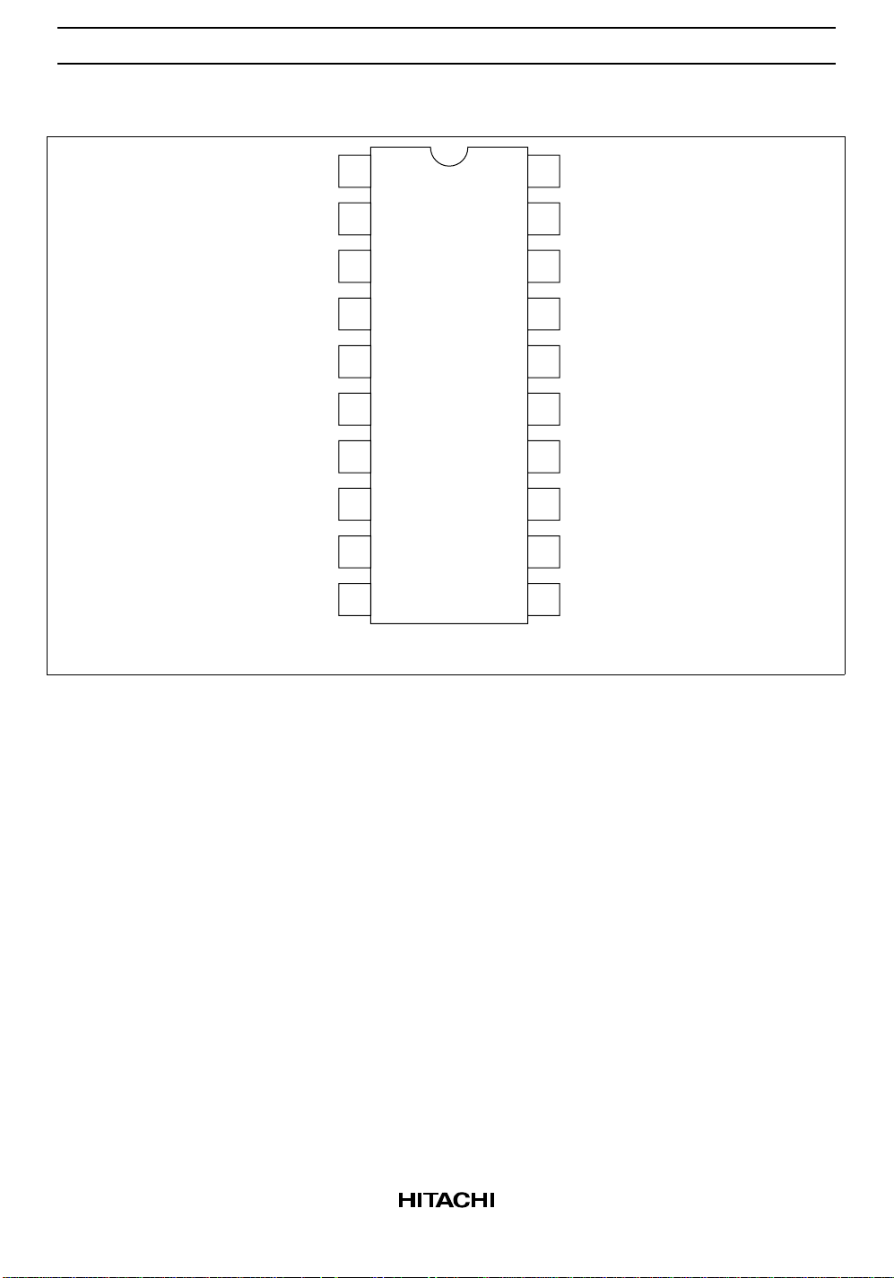
Pin Arrangement
HD74HC680
A
A
A
A
A
A
A
A
A
GND
1
1
2
2
3
3
4
4
5
5
6
6
7
7
8
8
9
9
10
20
19
18
17
16
15
14
13
12
11
V
CC
C
Y
P
3
P
2
P
1
P
0
A
12
A
11
A
10
(Top view)
3
 Loading...