HIT HD74HC674 Datasheet

HD74HC674
16-bit Shift Register
Description
The HD74HC674 is a 16-bit parallel-in, serial-out shift register. A three-state input/output (data I/O) port
provides access for entering serial data or reading the shift-register word in a recirculating loop.
The device has four basic modes of operation:
1. Hold (do nothing)
2. Write (serially via input/output)
3. Read (serially)
4. Load (parallel via data inputs)
Low-to-high-level changes at the chip select input should be made only when the clock input is low to
prevent false clocking.
Features
• High Speed Operation: tpd (CLK to SER/Q15) = 17 ns typ (CL = 50 pF)
• High Output Current: Fanout of 15 LSTTL Loads
• Wide Operating Voltage: VCC = 2 to 6 V
• Low Input Current: 1 µA max
• Low Quiescent Supply Current: ICC (static) = 4 µA max (Ta = 25°C)
Function Table
Inputs
CS R/W Mode CLK SER/Q
H X X X Z Do nothing
LLX Z Shift and write (serial load)
LHL Q
LHH P15Parallel load
14n
15
Operation
Shift and read

HD74HC674
Pin Arrangement
CLK
R/W
Mode
SER/Q
GND
CS
NC
15
P
P
P
P
P
1
2
3
4
5
6
7
0
8
1
9
2
10
3
11
4
12
24
23
22
21
20
19
18
17
16
15
14
13
V
CC
P
15
P
14
P
13
P
12
P
11
P
10
P
9
P
8
P
7
P
6
P
5
(Top view)
2

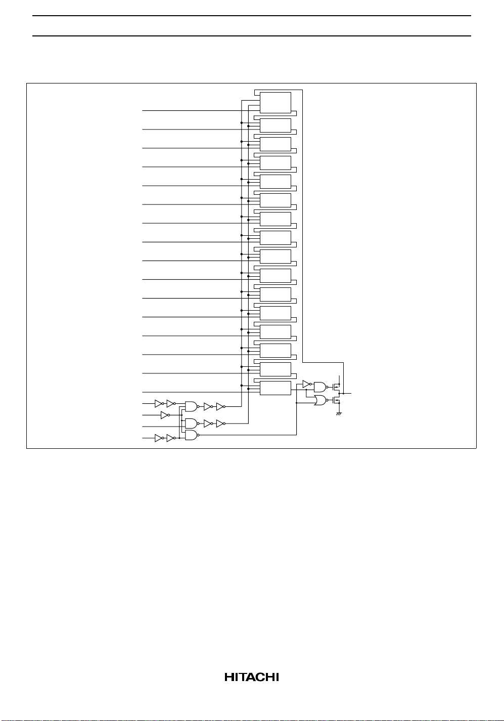
Logic Diagram
HD74HC674
IN
PE
CK
P
0
P
1
P
2
P
3
P
4
P
5
P
6
P
7
P
8
P
9
P
10
P
11
PQ
Mode
CLK
R/W
P
12
P
13
V
P
14
P
15
CC
SER/Q
15
CS
3
 Loading...