

HIT HD74HC673 Datasheet
HD74HC673
16-bit Shift Register
Description
The HD74HC673 is a 16-bit shift register and a 16-bit storage register in a single 24-pin package. A threestate input/output (data I/O) port to the shift register allows serial entry and/or reading of data. The storage
register is connected in a parallel data loop with the shift register and may be asynchronously cleared by
taking the store-clear input low. The storage register may be parallel loaded with shift-register data to
provide shift-register status via the parallel outputs. The shift register can be parallel loaded with the
storage-register data upon command.
A high logic level at the chip-select (CS) input disables both the shift-register clock and the storage register
clock and places the data I/O in the high-impedance state. The store-clear function is not disabled by the
chip select.
Caution must be exercised to prevent false clocking of either the shift register or the storage register via the
chip-select input. The shift clock should be low during the low-to-high transition of chip select and the
store clock should be low during the high-to-low transition of chip select.
Features
• High Speed Operation: tpd (MODE/STRCLK to Y) = 23 ns typ (CL = 50 pF)
• High Output Current: Fanout of 15 LSTTL Loads (Q15 output)
• Wide Operating Voltage: VCC = 2 to 6 V
• Low Input Current: 1 µA max
• Low Quiescent Supply Current: ICC (static) = 4 µA max (Ta = 25°C)
HD74HC673
Function Table
Inputs Shift Register Functions Storage Register
Mode/ SER/ Read from Write into Parallel Functions
CS R/W SHCLK STRCLR STRCLK Q
H X X X X Z No No No No No
X X X L X Yes
LL X X Z Yes No Yes No
LHX X X Q
LH XL Q
LH L H L No Yes Yes Yes No
LH HHY
LLX H Z No No No Yes
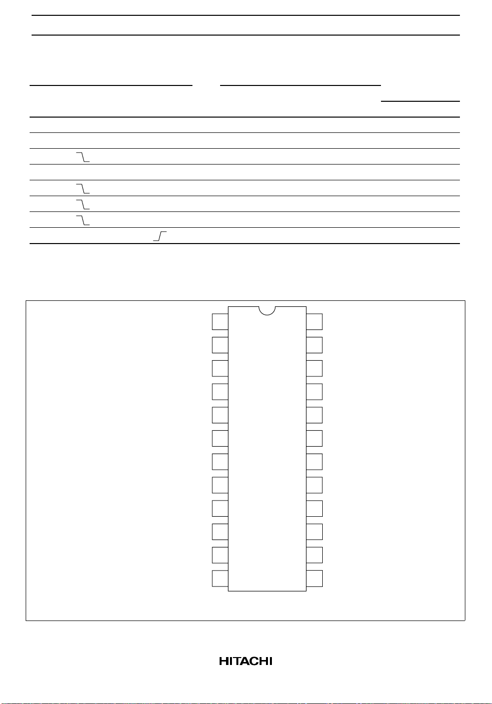
Pin Arrangement
Shift Serial Output Serial Input Load Clear Load
15
15
14n
15n
Yes No No
Yes Yes No No No
No Yes Yes No No
CS
SH CLK
R/W
STRCLR
Mode/STRCLK
SER/Q
Y
Y
Y
Y
Y
GND
1
2
3
4
5
6
15
7
0
8
1
9
2
10
3
11
4
12
24
23
22
21
20
19
18
17
16
15
14
13
V
CC
Y
15
Y
14
Y
13
Y
12
Y
11
Y
10
Y
9
Y
8
Y
7
Y
6
Y
5
(Top view)
2
HD74HC673
Absolute Maximum Ratings
Item Symbol Rating Unit
Supply voltage range V
Input voltage V
Output voltage V
Output current I
DC current drain per VCC, GND ICC, I
DC input diode current I
DC output diode current I
Power dissipation per package P
CC
IN
OUT
OUT
GND
IK
OK
T
Storage temperature Tstg –65 to +150 °C
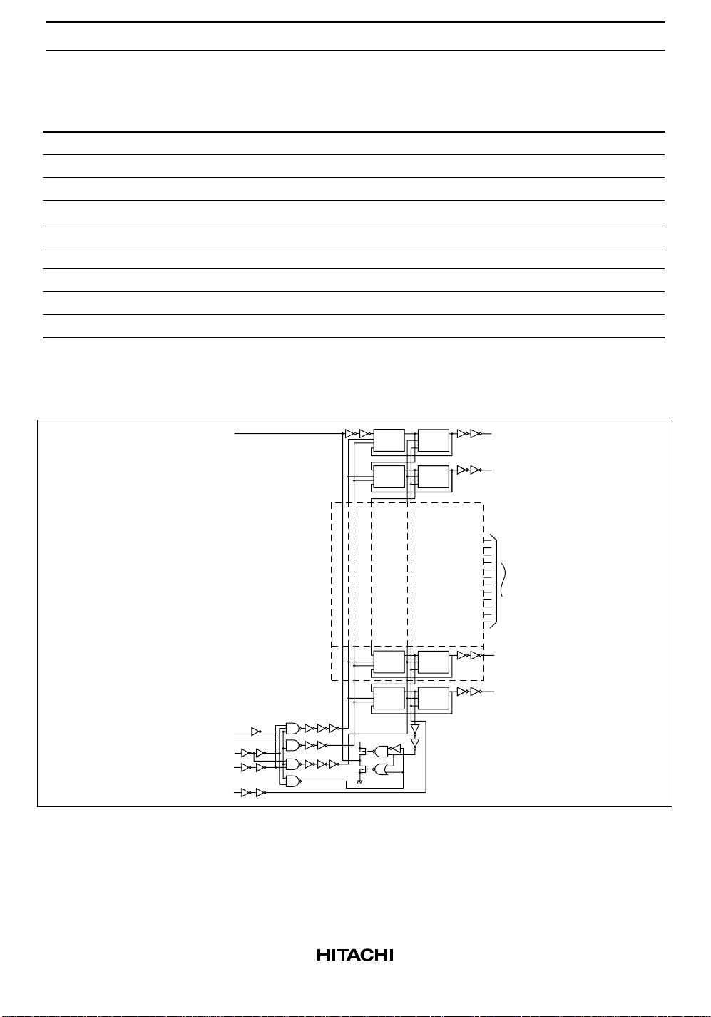
Logic Diagram
–0.5 to +7.0 V
–0.5 to VCC + 0.5 V
–0.5 to VCC + 0.5 V
±35 mA
±75 mA
±20 mA
±20 mA
500 mW
SER Q
CS
SHCLK
R W
M S
STRCLR
15
IN
PE
SCK
P
V
CC
DYQ
CK
CLR
X
12
Y
0
Y
1
Y
2
Y
13
Y
14
Y
15
3
 Loading...