HIT HD74HC670 Datasheet

HD74HC670
4-by-4 Register File (with 3-state outputs)
Description
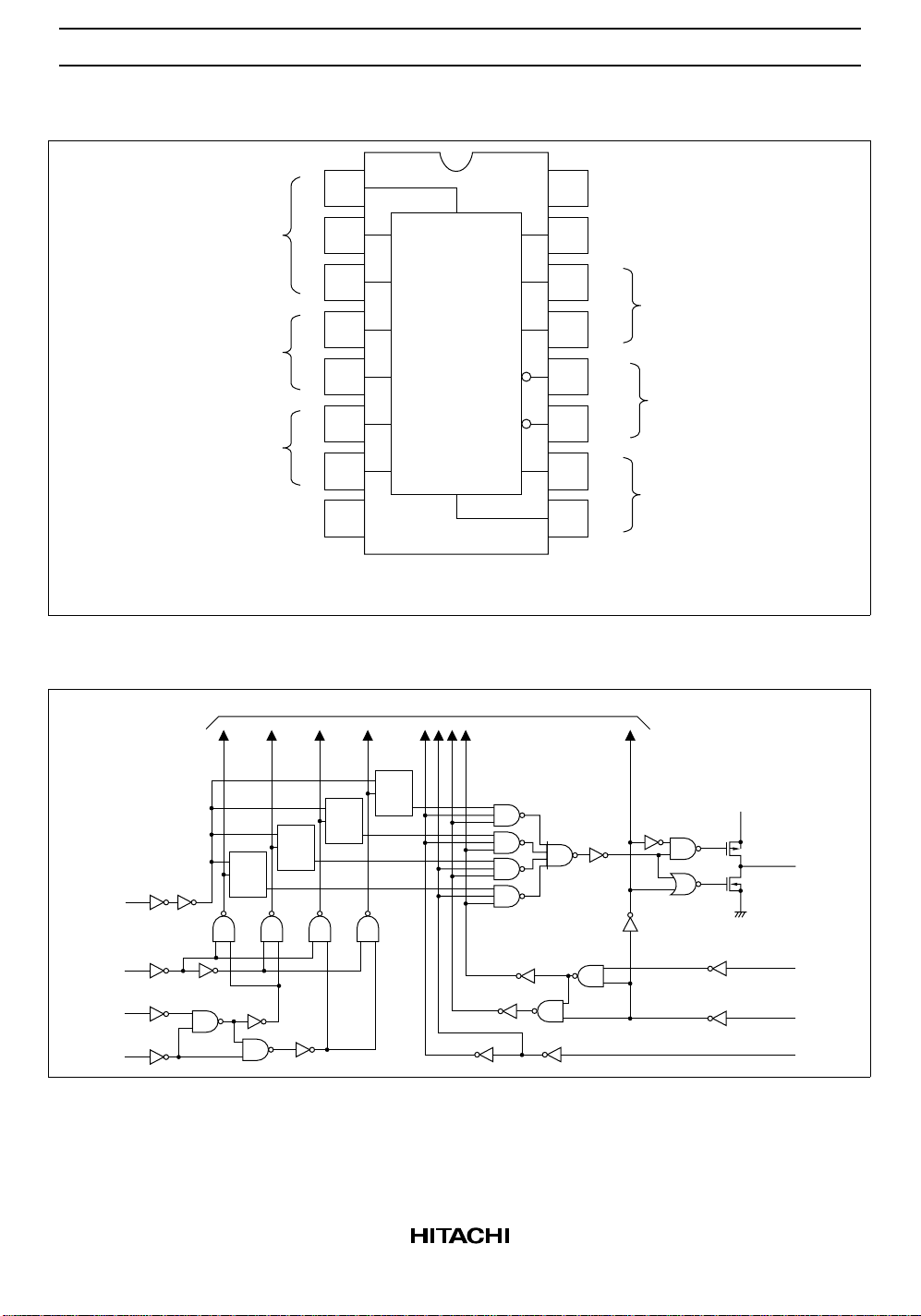
The HD74HC670, 16-bit register file is organized as 4 words of 4 bits each and separate on-chip decoding
is provided for addressing the four word locations to either write-in or retrieve data.
This permits simultaneous writing into one location and reading from another word location. Four data
inputs are available which are used to supply the 4-bit word to be stored. Location of the word is
determined by the write-address inputs A and B in conjunction with a write-enable signal. Data applied at
the inputs should be in its true form. That is, if a high-level signal is desired from the output, a high-level is
applied at the data input for that particular bit location. The latch inputs are arranged so that new data will
be accepted only if both internal address gate inputs are high. When this condition exists, data at the D
input is transferred to the latch output. When the write-enable input, (GW) is high, the data inputs are
inhibited and their levels can cuase no change in the information stored in the internal latches. When the
read-enable input, (GR) is high, the data outputs are inhibited and go into the high-impedance state. The
individual address lines permit direct acquisition of data stored in any four of the latches. Four individual
decoding gates are used to complete the address for reading a word. when the read address is made in
conjunction with the read-enable signal, the word appears at the four outputs.
Features
• High Speed Operation: tpd (Read Select to Q) = 21 ns typ (CL = 50 pF)
• High Output Current: Fanout of 15 LSTTL Loads
• Wide Operating Voltage: VCC = 2 to 6 V
• Low Input Current: 1 µA max
• Low Quiescent Supply Current: ICC (static) = 4 µA max (Ta = 25°C)

HD74HC670
Function Table
Write Inputs Word
W
B
W
A
L L L Q = D Q
LH L Q
HL L Q
HH L Q
XX H Q
Read Inputs Outputs
R
B
R
A
LL L W
LH L W
HL L W
HH L W
XXHZZZZ
H : high level
L : low level
X : irrelevant
Z : high impedance (off)
(Q = D) : The four selected internal flip-flop outputs will assume the states applied to the four external data
inputs.
Q
: The level of Q before the indicated input conditions were established.
0
W
: The first bit of word 0, etc.
0 B1
G
W
G
R
0123
0
0
0
0
Q
1
0 B1
1 B1
2 B1
3 B1
0
Q = D Q
Q
0
Q
0
Q
0
Q
2
W0 B
2
W1 B
2
W2 B
2
W3 B
2
Q
0
0
Q = D Q
Q
0
Q
0
Q
3
W0 B
3
W1 B
3
W2 B
3
W3 B
3
Q
0
Q
0
0
Q = D
Q
0
Q
4
W0 B
4
W1 B
4
W2 B
4
W3 B
4
2

Pin Arrangement
HD74HC670
V
1
D
2
16
CC
Logic Diagram
Data
Read
select
Outputs
D
D
R
R
Q
Q
GND
D
2
3
3
4
4
B
5
A
D
D
R
R
2
D
W
W
C
1
A
B
W
3
4
B
A
15
14
13
12
Data
D
1
W
A
W
B
Write
Write
select
Enable
Read
6
4
7
3
Q
4
Q
3
C
Q
Q
2
8
11
R
Q
10
1
1
Outputs
Q
9
2
(Top view)
To other three bits
Data
D
G
D
G
D
G
D
G
W
A
W
B
G
W
Q
Q
Q
Q
V
CC
Q
R
A
G
R
R
B
3
 Loading...