HIT HD74HC648, HD74HC646 Datasheet

HD74HC646/HD74HC648
Octal Bus Transceivers/Registers with Multiplexed 3-state outputs
Description
Six control inputs enable this device to be used as a latched transceiver, unlatched transceiver or a
combination of both. As a latched transceiver, data from one bus is stored for later retrieval by the other
bus. Alternately real time bus data (unlatched) may be directly transferred from one bus to another.
Circuit operation is determined by the Control G, Direction, Clock AB, Clock BA, Select AB, Select BA
control inputs. The enable input, Contorl G, controls whether any bus outputs are enabled. The direction
control Direction (DIR), determines which bus is enabled, and hence the direction data flows: The Select
AB, Select BA inputs cotrol whether the latched data (stored in D type flip-flops), or the bus data (from
other bus input pins) is transferred. Each set of flip-flops has its own clock Clock AB and Clock BA, for
storing data. Data is latched on the rising edge of the clock.
Features
• High Speed Operation: tpd (Bus to Bus) = 14 ns typ (CL = 50 pF)
• High Output Current: Fanout of 15 LSTTL Loads
• Wide Operating Voltage: VCC = 2 to 6 V
• Low Input Current: 1 µA max
• Low Quiescent Supply Current: ICC (static) = 4 µA max (Ta = 25°C)

HD74HC646/HD74HC648
Function Table
Inputs
Control Clock Select Data I/O Data I/O Operation or Function
G Direction BA AB AB BA A1 thru A8 B1 thru B8 HD74HC646 HD74HC648
H X X X X X Z (Input) Z (Input) Isolation Isolation
HX H H Z (Input) Z (Input) Store A & B data Store A & B data
L L X X X L Output Z (Input) B real-time data to
A bus
L L H H X H Output Z (Input) B stored data to A
bus
L L LLXHOutput Z (Input) B stored data to A
bus
L H X X L X Z (Input) Output A real-time data to
B bus
L H H H H X Z (Input) Output A stored data to B
bus
L H L L H X Z (Input) Output A stored data to B
bus
B real-time data to
A bus
B stored data to A
bus
B stored data to A
bus
A real-time data to
B bus
A stored data to B
bus
A stored data to B
bus
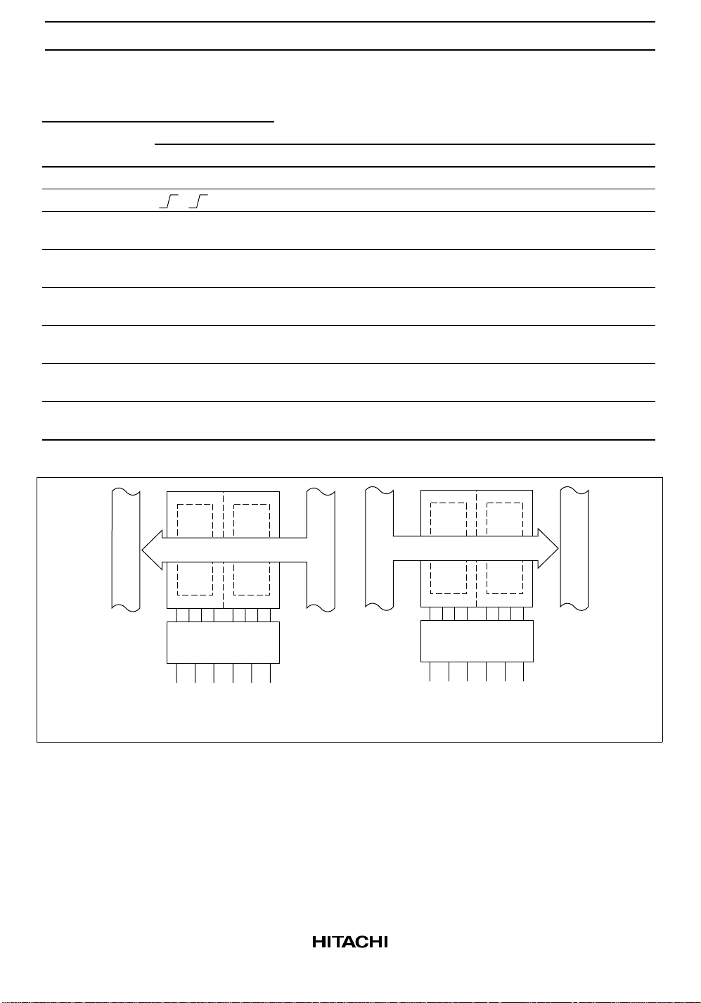
Bus A
Bus B
Real-time transfer
Bus B to Bus A
2
Bus A
Real-time transfer
Bus A to Bus B
Bus B

HD74HC646/HD74HC648
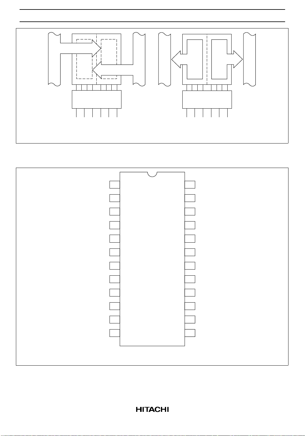
Bus A
Pin Arrangement
Storage from
A, B, or A and B
Clock AR
Select AB
Direciton
A
1
A
2
Bus B
Bus A
Bus B
Transfer stored data
to A or B
1
2
3
4
5
24
23
22
21
20
V
CC
Clock BA
Select BA
Control G
B
1
A
A
A
A
A
A
GND
6
3
7
4
8
5
9
6
10
7
11
8
12
19
18
17
16
15
14
13
B
2
B
3
B
4
B
5
B
6
B
7
B
8
(Top view)
3
 Loading...