

HIT HD74HC640 Datasheet
HD74HC640/HD74HC643
Octal Bus Transceivers (with 3-state outputs)
Description
Each device has an active enable G and a direction control input, DIR. when DIR is high, data flows from
the A inputs to the B outputs. When DIR is low, data flows from the B inputs to the A outputs. The
HD74HC640 transfers inverted data from one bus to other and the HD74HC643 transfers inverted data
from the A bus to the B bus and true data from the B bus to the A bus.
Features
• High Speed Operation: tpd = 12 ns typ (CL = 50 pF)
• High Output Current: Fanout of 15 LSTTL Loads
• Wide Operating Voltage: VCC = 2 to 6 V
• Low Input Current: 1 µA max
• Low Quiescent Supply Current: ICC (static) = 4 µA max (Ta = 25°C)
Function Table
Control Inputs Operation
G DIR HD74HC640 HD74HC643
LLB data to A bus B data to A bus
LHA data to B bus A data to B bus
H X Isolation Isolation
HD74HC640/HD74HC643
G
Pin Arrangement
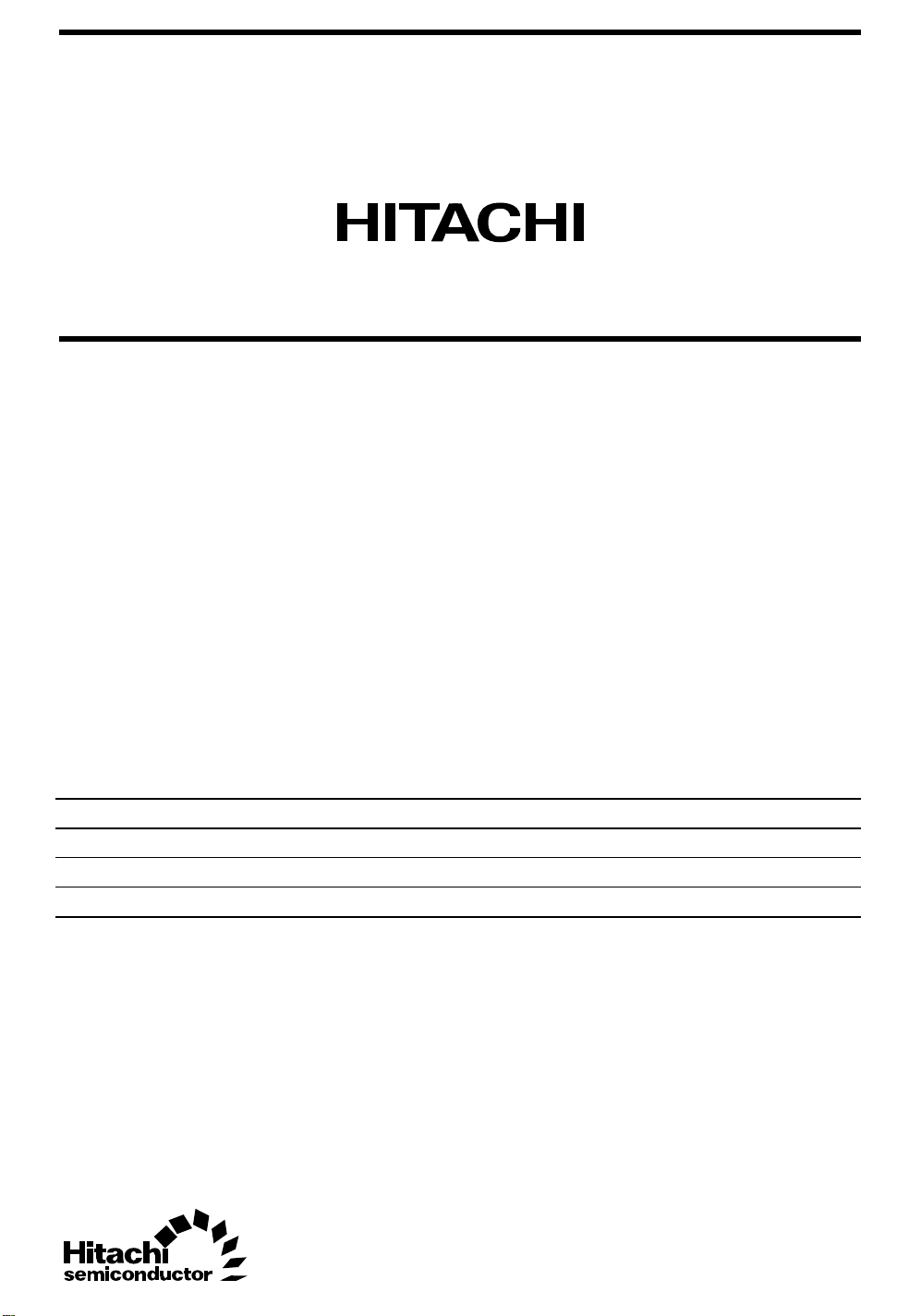
HD74HC640
1
DIR VCC
A1
2
A2
3
A3
4
A4
5
A5
6
A6
7
A7
8
A8
9
GND
10 11
(Top View)
20
19
18
17
16
15
14
13
12
Enable
B1
B2
B3
B4
B5
B6
B7
B8
2
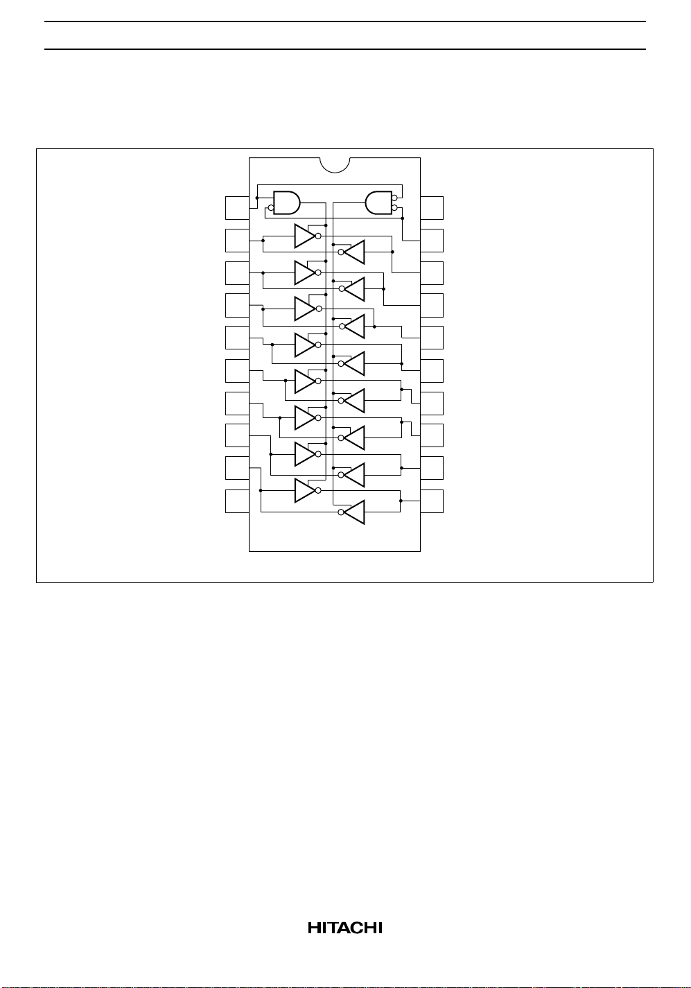
HD74HC643
G
HD74HC640/HD74HC643
1
DIR VCC
A1
2
A2
3
A3
4
A4
5
A5
6
A6
7
A7
8
A8
9
GND
10 11
Absolute Maximum Ratings
(Top View)
20
19
18
17
16
15
14
13
12
Enable
B1
B2
B3
B4
B5
B6
B7
B8
Item Symbol Rating Unit
Supply voltage range V
Input voltage V
Output voltage V
Output current I
CC
IN
OUT
OUT
DC current drain per VCC , GND ICC, I
DC input diode current I
DC output diode current I
Power Dissipation per package P
IK
OK
T
GND
–0.5 to +7.0 V
–0.5 to VCC + 0.5 V
–0.5 to VCC + 0.5 V
±35 mA
±75 mA
±20 mA
±20 mA
500 mW
Storage temperature Tstg –65 to +150 °C
3
HD74HC640/HD74HC643
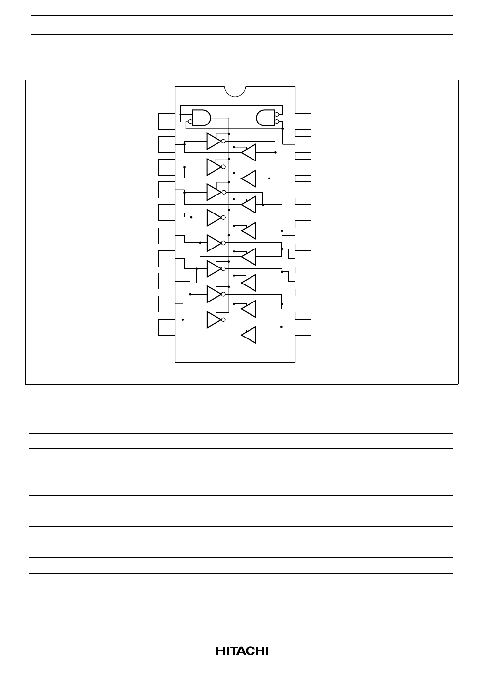
Block Diagram
HD74HC640
G
DIR
A
VCC
CC
V
B
To 7 Other
Inverters
To 7 Other
Inverters
4
 Loading...