HIT HD74HC623, HD74HC620 Datasheet

HD74HC620/HD74HC623
Octal Bus Transceivers (with inverted 3-state outputs)
Octal Bus Transceivers (with 3-state outputs)
Description
This octal bus transceiver is designed for asynchronous two-way communication between data buses. The
control fuction implementation allows for maximum flexibility in timing.
This device allows data transmission from the A bus to the B bus or from the B bus to the A bus depending
upon the logic levels at the enable inputs (GBA and GAB).
The enable inputs can be used to disable the device so that the buses are effectively isolated.
The dual-enable configuration gives these devices the capability to store data by simultaneous enabling of
GBA and GAB. Each output reinforces its input in this transceiver configuration. Thus, when both control
inputs are enabled and all other data sources to the two sets of bus lines are at high impedance, both sets of
bus lines (16 in all) will remain at their last states. The 8-bit codes appearing on the two sets of buses will
be identical for the HD74HC623 or coplementary for the HD74HC620.
Features
• High Speed Operation: tpd (Bus to Bus) = 12 ns typ (CL = 50 pF)
• High Output Current: Fanout of 15 LSTTL Loads
• Wide Operating Voltage: VCC = 2 to 6 V
• Low Input Current: 1 µA max
• Low Quiescent Supply Current: ICC (static) = 4 µA max (Ta = 25°C)
Function Table
Enable Inputs Operation
GBA GAB HD74HC620 HD74HC623
LLB data to A bus B data to A bus
HHA data to B bus A data to B bus
H L Isolation Isolation
LHB data to A bus, A data to B bus B data to A bus, A data to B bus

HD74HC620/HD74HC623
Pin Arrangement
Enable GAB V
A1
A2
A3
A4
A
A6
A7
A8
GND
Absolute Maximum Ratings
1
2
3
4
5
5
6
7
8
9
10 11
(Top view)
20
CC
Enable GBA
19
18
1
B
17
B2
16
B3
15
B
4
14
B5
13
B6
12
B7
B8
Item Symbol Rating Unit
Supply voltage range V
Input voltage V
Output voltage V
Output current I
CC
IN
OUT
OUT
DC current drain per VCC GND ICC, I
DC input diode current I
DC output diode current I
Power Dissipation per package P
IK
OK
T
GND
–0.5 to +7.0 V
–0.5 to VCC + 0.5 V
–0.5 to VCC + 0.5 V
±35 mA
±75 mA
±20 mA
±20 mA
500 mW
Storage temperature Tstg –65 to +150 °C
2

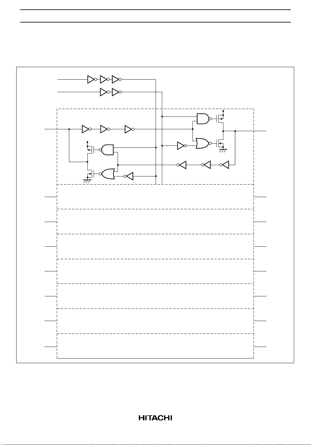
Block Diagram
HD74HC620
GBA
GAB
HD74HC620/HD74HC623
VCC
A1
A2
A3
A4
A5
A6
B1
VCC
B2
B3
B4
B5
B6
A7
B7
B8A8
3
 Loading...