HIT HD74HC597 Datasheet

HD74HC597
8-bit Latch/Shift Register
Description
The HD74HC597 consists of an 8-bit storage latch feeding a parallel-in, serial-out 8-bit shift register. Both
the storage register and shift register have positive-edge triggered clocks. The shift register also has direct
load (from storage) and clear inputs.
Features
• High Speed Operation: tpd (SCK to QH’) = 14 ns typ (CL = 50 pF)
• High Output Current: Fanout of 10 LSTTL Loads
• Wide Operating Voltage: VCC = 2 to 6 V
• Low Input Current: 1 µA max
• Low Quiescent Supply Current: ICC (static) = 4 µA max (Ta = 25°C)
Function Table
RCK SCK SLoad SCLR Function
X X X Data loaded to input latches
X L H Data loaded from inputs to shift register
X X L H Data transferred from input latches to shift register
X X L L Invalid logic, state of shift register indeterminate when signals
removed
X X H L Shift register cleared
X H H Shift register clocked Qn = Q
, QA = SER
n – 1

HD74HC597
Pin Arrangement
1
BV
2
C
3
D
4
E
F
5
G
6
7
H
89
GND
(Top view)
16
15
14
13
12
11
10
CC
A
SER
S Load
RCK
SCK
SCLR
Q'
H
2

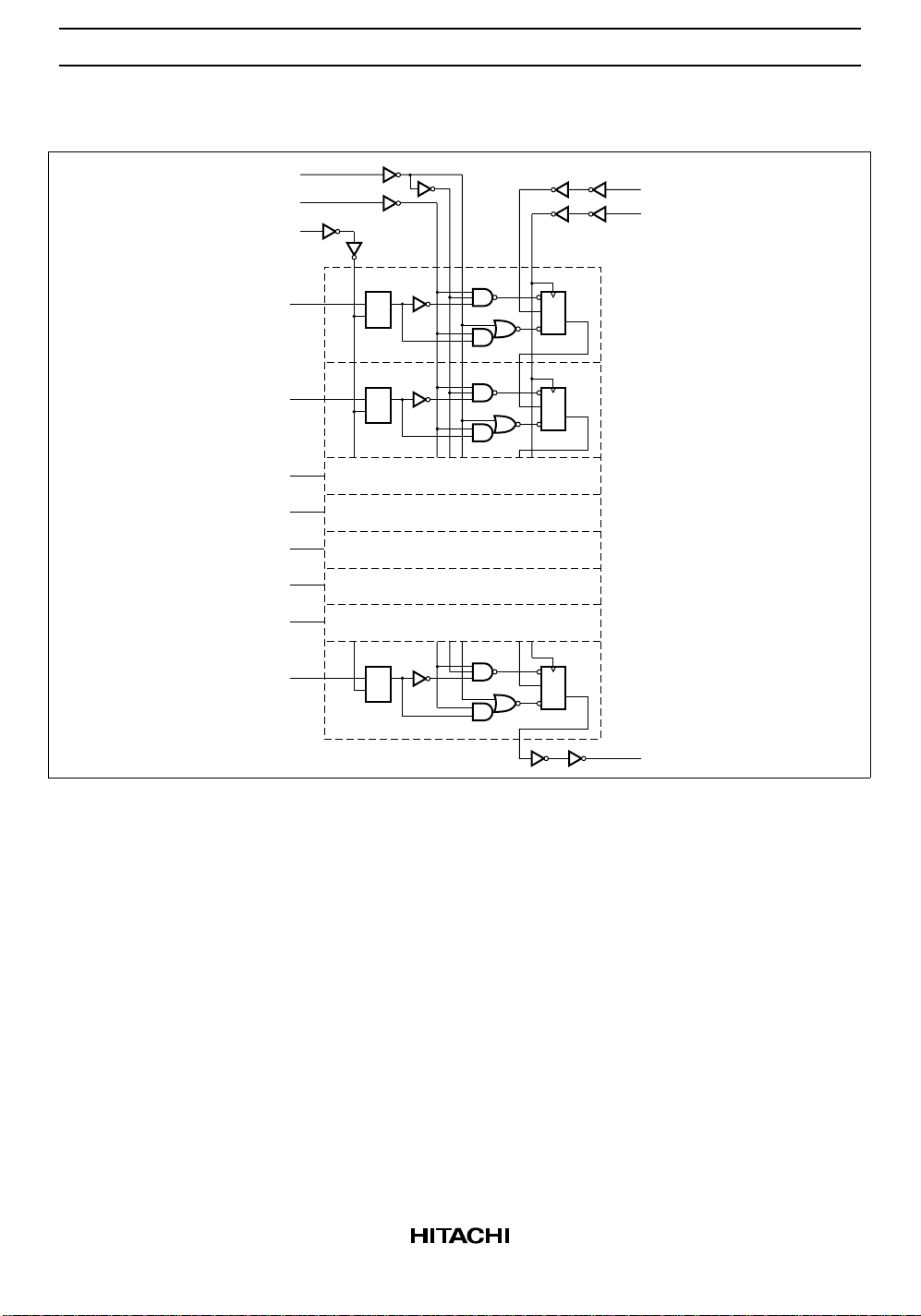
Logic Diagram
HD74HC597
SCLR
SLoad
RCK
A
B
C
D
E
F
G
H
SER
SCK
S
QD
C
QD
C
Q
D
C
C
D
Q
R
S
C
D
Q
R
S
C
D
Q
R
Q'H
3
 Loading...