HIT HD74HC595 Datasheet

HD74HC595
8-bit Shift Register/Latch (with 3-state outputs)
Description
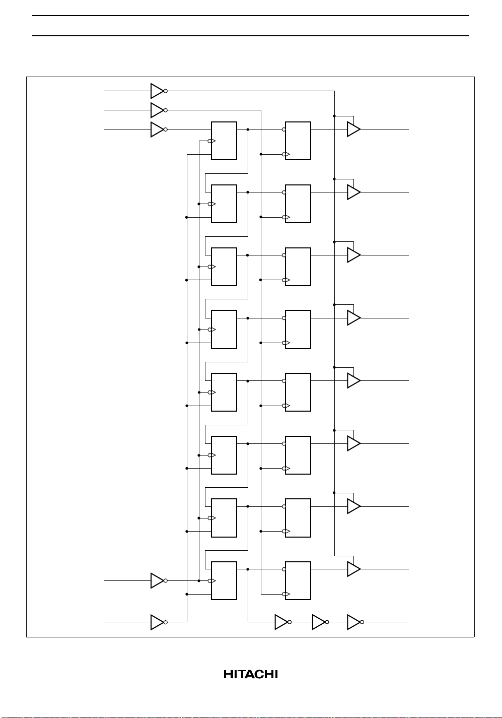
This device each contains an 8-bit serial-in, parallel-out shift register that feeds an 8-bit D-type storage
register. The storage register has parallel 3-state outputs. Separate clocks are provided for both the shift
register and the storage register. The shift register has a direct-overriding clear, serial input, and serial
output pins for cascading.
Both the shift register and storage register clocks are positive-edge triggered. If the user wishes to connect
both clocks together, the shift register state will always be one clock pulse ahead of the storage register.
Features
• High Speed Operation: tpd (RCK to Q) = 17 ns typ (CL = 50 pF)
• High Output Current: Fanout of 15 LSTTL Loads (QA to QH outputs)
• Wide Operating Voltage: VCC = 2 to 6 V
• Low Input Current: 1 µA max
• Low Quiescent Supply Current: ICC (static) = 4 µA max (Ta = 25°C)
Function Table
RCK SCK SCLR G Function
XXXHQ
X X L X Shift register cleared QH’ = L
X H X Shift register clocked Qn = Q
X H X Contents of shift register transferred to output latches
to QH high impedance
A
, QA = SER
n – 1

HD74HC595
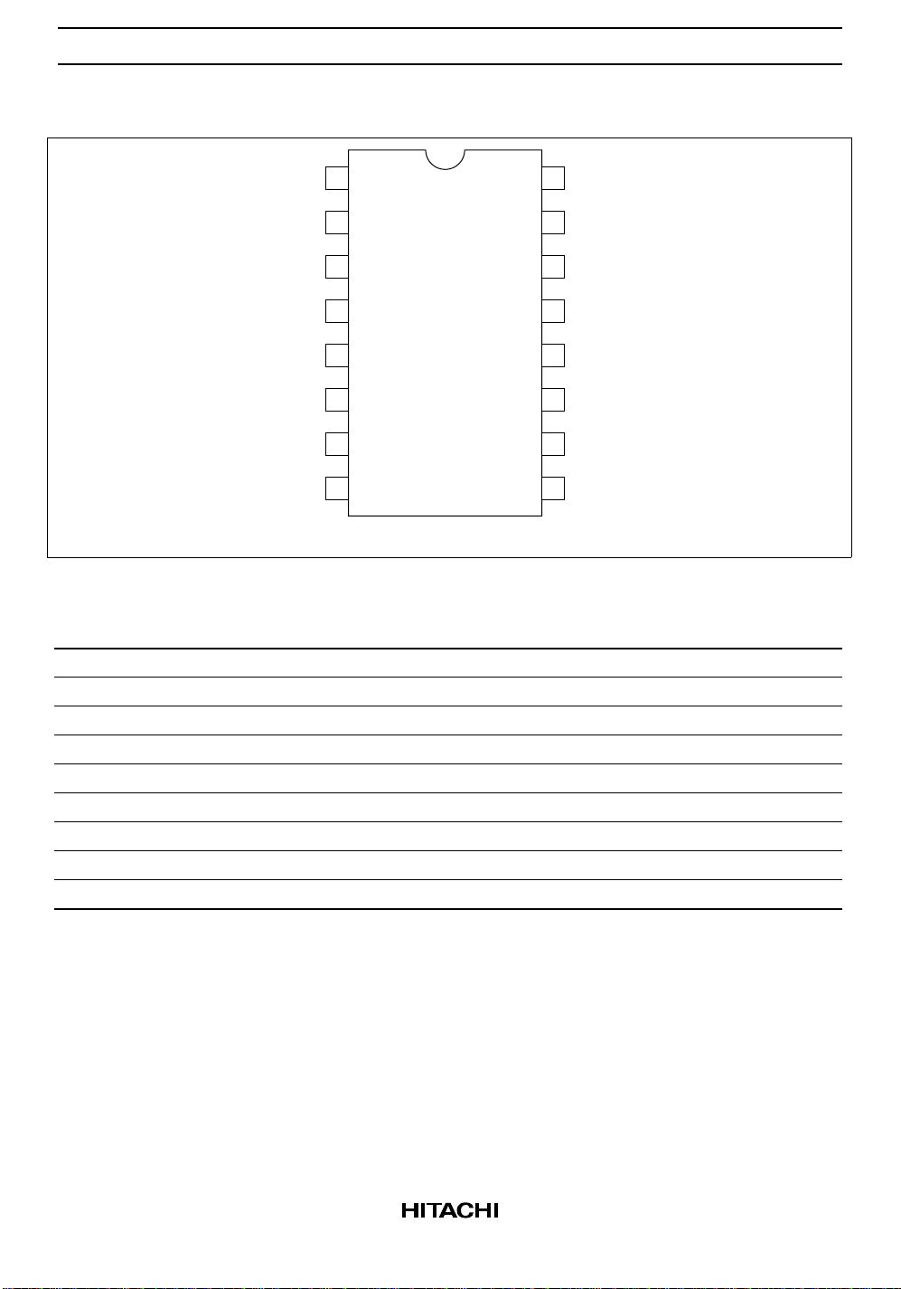
Pin Arrangement
1
Q
B VCC
2
C
Q
QD
3
QE
4
QF
5
QG
6
7
QH
GND
89
16
15
14
13
12
11
10
QA
SER
G
RCK
SCK
SCLR
H'
Q
(Top view)
Absolute Maximum Ratings
Item Symbol Rating Unit
Supply voltage range V
Input voltage V
Output voltage V
Output current I
DC current drain per VCC, GND ICC, I
DC input diode current I
DC output diode current I
Power dissipation per package P
CC
IN
OUT
OUT
GND
IK
OK
T
Storage Temperature Tstg –65 to +150 °C
–0.5 to +7.0 V
–0.5 to VCC + 0.5 V
–0.5 to VCC + 0.5 V
±35 mA
±75 mA
±20 mA
±20 mA
500 mW
2

Logic Diagram
G
RCK
HD74HC595
SER
R
R
R
R
R
DDQ
DDQ
DDQ
DDQ
DDQ
QA
QB
QC
QD
QE
SCK
SCLR
R
R
R
DDQ
DDQ
DDQ
QF
QG
Q
H
H'
Q
3
 Loading...