HIT HD74HC589 Datasheet

HD74HC589
8-bit Serial of Parallel-input/Serial-output Shift Register
(with 3-state outputs)
Description
The HD74HC589 is similar in function to the HD74HC597, which is not a 3-state device.
This device consists of an 8-bit storage latch which feeds parallel data to an 8-bit shift register. Data can
also be loaded serially (see Function Table). The shift register output, OH, is a three-state output, allowing
this device to be used in bus-oriented systems.
Features
• High Speed Operation: tpd (Shift Clock to QH) = 15 ns typ (CL = 50 pF)
• High Output Current: Fanout of 15 LSTTL Loads
• Wide Operating Voltage: VCC = 2 to 6 V
• Low Input Current: 1 µA max
• Low Quiescent Supply Current: ICC (static) = 4 µA max (Ta = 25°C)
Function Table
Latch Clock
LCK
X X L L Data are transfered from input
L, H, L, H, X H Outputs are disabled
X H L Serial shift Qn = Q
Shift Clock
SCK
X X X Data are loaded into input latches
X L L Data are loaded from input into shift
Serial Shift/
Parallel Load
Output EnableOEFunction
registers
latches to shift registers
, Q0 = SER
n – 1

HD74HC589
Pin Arrangement
1
BV
2
C
D
3
E
4
F
5
G
6
7
H
GND
89
16
CC
A
15
14
A
S
Serial Shift/
13
Parallel Load
12
Latch Clock
11
Shift Clock
10
Output Enable
H
Q
(Top view)
Absolute Maximum Ratings
Item Symbol Rating Unit
Supply voltage range V
Input voltage V
Output voltage V
Output current I
DC current drain per VCC, GND ICC, I
DC input diode current I
DC output diode current I
Power Dissipation per package P
CC
IN
OUT
OUT
GND
IK
OK
T
Storage temperature Tstg –65 to +150 °C
–0.5 to +7.0 V
–0.5 to VCC + 0.5 V
–0.5 to VCC + 0.5 V
±35 mA
±75 mA
±20 mA
±20 mA
500 mW
2

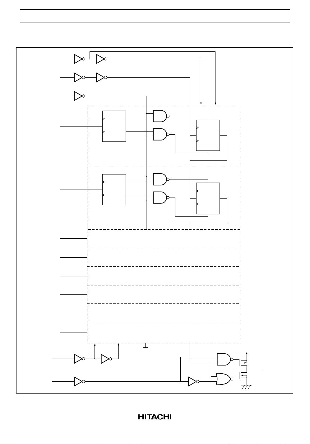
Logic Diagram
SCK
S
A
Shift/
Load
A
LCK
D
LCK
HD74HC589
SCK
D
SCK
SCK
S
Q
R
SCK
Q
Q
LCK
LCKDQ
B
C
D
E
F
G
H
LCK
LCK
Q
LCK
SCK
D
SCK
S
Q
R
VCC
OE
Q
H
3
 Loading...