HIT HD74HC573, HD74HC563 Datasheet

HD74HC563/HD74HC573
Octal Transparent Latches (with 3-state outputs)
Description
When the latch enable (LE) input is high, the Q outputs of HD74HC563 will follow the inversion of the D
inputs and the Q outputs of HD74HC573 will follow the D inputs. When the latch enable goes low, data at
the D inputs will be retained at the outputs until latch enable returns high again. When a high logic level is
applied to the output control input, all outputs go to a high impedance state, regardless of what signals are
present at the other inputs and the state of the storage elements.
Features
• High Speed Operation: tpd (Data to Q, Q) = 11 ns typ (CL = 50 pF)
• High Output Current: Fanout of 15 LSTTL Loads
• Wide Operating Voltage: VCC = 2 to 6 V
• Low Input Current: 1 µA max
• Low Quiescent Supply Current: ICC (static) = 4 µA max (Ta = 25°C)
Function Table
Outputs
Output Control Latch Enable Data HD74HC563 HD74HD573
LHHLH
LHLHL
LL XQ
HX XZZ
Q
: level of Q before the indicated Steady-sate input conditions were established.
0
Q
: complement of Q0 or level of Q before the indicated Steady-state input conditions were established.
0
0
Q
0

HD74HC563/HD74HC573
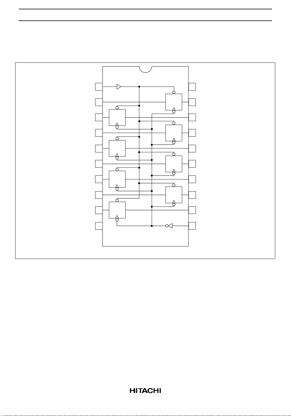
Pin Arrangement
HD74HC563
Output
Control
1D
2D
3D
4D
5D
6D
7D
8D
GND
10
1
2
OE
3
D Q
4
OE
5
D Q
6
OE
7
D Q
8
OE
9
D Q
(Top view)
OE
D Q
OE
D Q
OE
D Q
OE
D Q
20
19
18
17
16
15
14
13
12
11
VCC
1Q
2Q
3Q
4Q
5Q
6Q
7Q
8Q
Latch
Enable
2

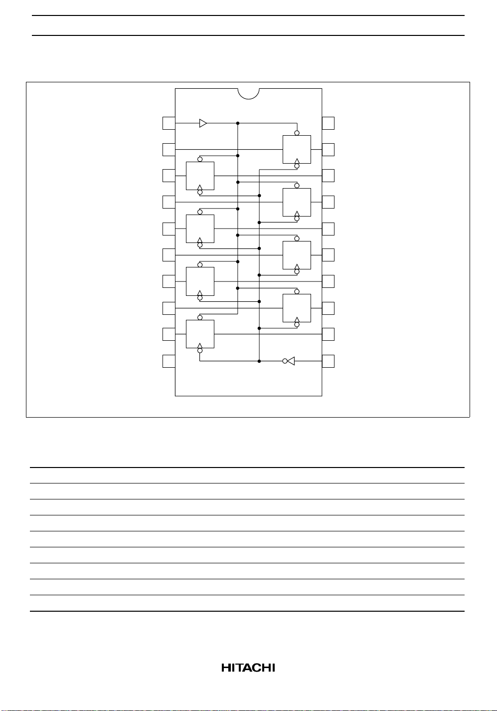
HD74HC573
HD74HC563/HD74HC573
Output
Control
1D
2D
3D
4D
5D
6D
7D
8D
GND
1
2
3
4
5
6
7
8
9
10
OE
DQ
OE
DQ
OE
DQ
OE
DQ
(Top view)
OE
DQ
OE
DQ
OE
DQ
OE
DQ
20
19
18
17
16
15
14
13
12
11
VCC
1Q
2Q
3Q
4Q
5Q
6Q
7Q
8Q
Latch
Enable
Absolute Maximum Ratings
Item Symbol Rating Unit
Supply voltage range V
Input voltage V
Output voltage V
Output current I
DC current drain per VCC , GND ICC, I
DC input diode current I
DC output diode current I
Power Dissipation per package P
CC
IN
OUT
OUT
GND
IK
OK
T
Storage temperature Tstg –65 to +150 °C
–0.5 to +7.0 V
–0.5 to VCC + 0.5 V
–0.5 to VCC + 0.5 V
±35 mA
±75 mA
±20 mA
±20 mA
500 mW
3

HD74HC563/HD74HC573
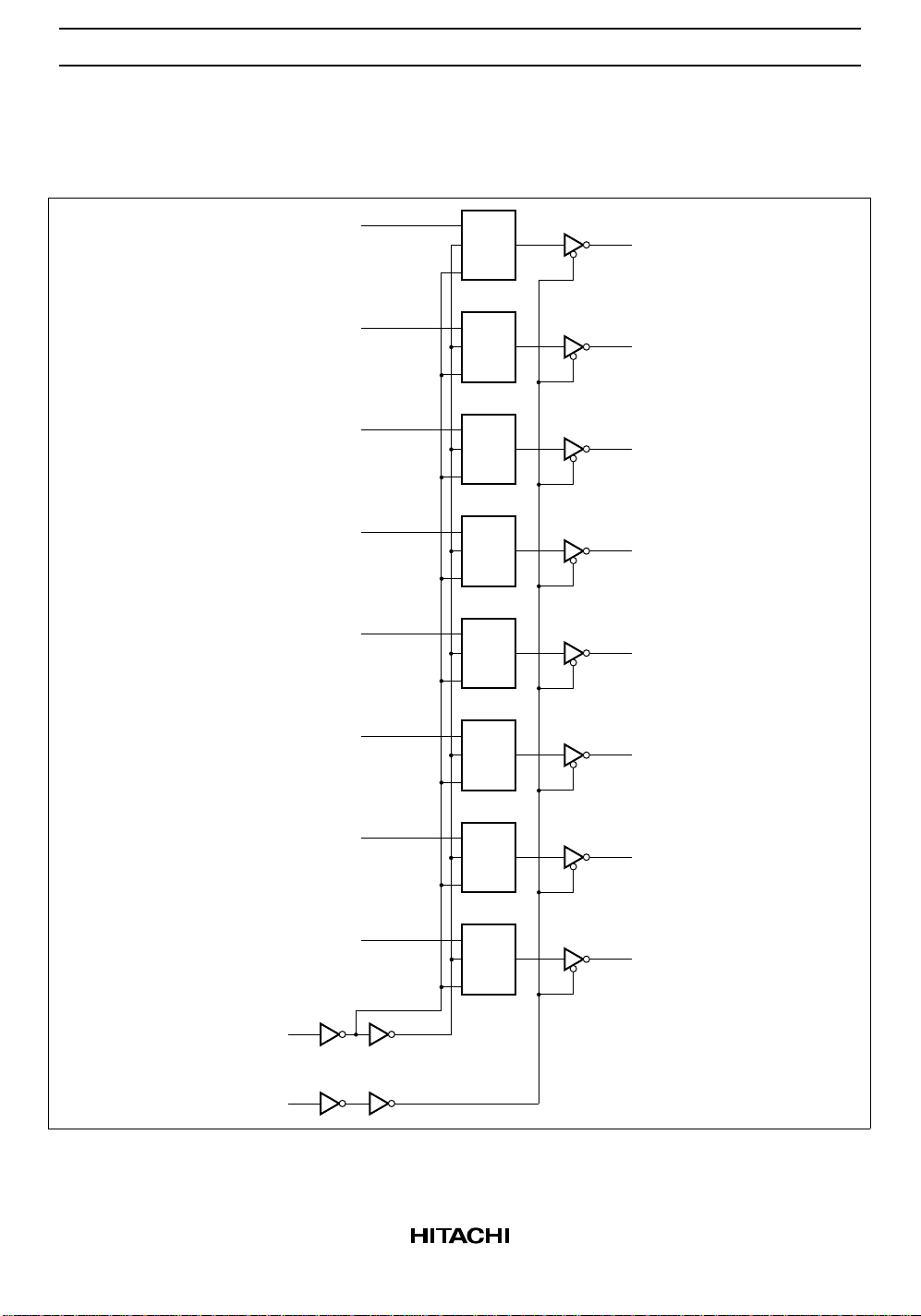
Block Diagram
HD74HC563
1D
2D
3D
4D
5D
6D
D
Q
C
C
D
Q
C
C
D
Q
C
C
D
Q
C
C
D
Q
C
C
D
Q
C
C
1Q
2Q
3Q
4Q
5Q
6Q
7D
8D
LE
OC
4
D
Q
C
C
D
Q
C
C
7Q
8Q
 Loading...